EP2319954A1 - Procédé pour la fabrication d'une couche mince de CIS et/ou de CIGS sur des substrats de verre - Google Patents
Procédé pour la fabrication d'une couche mince de CIS et/ou de CIGS sur des substrats de verre Download PDFInfo
- Publication number
- EP2319954A1 EP2319954A1 EP10011072A EP10011072A EP2319954A1 EP 2319954 A1 EP2319954 A1 EP 2319954A1 EP 10011072 A EP10011072 A EP 10011072A EP 10011072 A EP10011072 A EP 10011072A EP 2319954 A1 EP2319954 A1 EP 2319954A1
- Authority
- EP
- European Patent Office
- Prior art keywords
- temperature
- furnace
- substrates
- copper
- indium
- Prior art date
- Legal status (The legal status is an assumption and is not a legal conclusion. Google has not performed a legal analysis and makes no representation as to the accuracy of the status listed.)
- Withdrawn
Links
Images





Classifications
-
- C—CHEMISTRY; METALLURGY
- C23—COATING METALLIC MATERIAL; COATING MATERIAL WITH METALLIC MATERIAL; CHEMICAL SURFACE TREATMENT; DIFFUSION TREATMENT OF METALLIC MATERIAL; COATING BY VACUUM EVAPORATION, BY SPUTTERING, BY ION IMPLANTATION OR BY CHEMICAL VAPOUR DEPOSITION, IN GENERAL; INHIBITING CORROSION OF METALLIC MATERIAL OR INCRUSTATION IN GENERAL
- C23C—COATING METALLIC MATERIAL; COATING MATERIAL WITH METALLIC MATERIAL; SURFACE TREATMENT OF METALLIC MATERIAL BY DIFFUSION INTO THE SURFACE, BY CHEMICAL CONVERSION OR SUBSTITUTION; COATING BY VACUUM EVAPORATION, BY SPUTTERING, BY ION IMPLANTATION OR BY CHEMICAL VAPOUR DEPOSITION, IN GENERAL
- C23C14/00—Coating by vacuum evaporation, by sputtering or by ion implantation of the coating forming material
- C23C14/58—After-treatment
- C23C14/5846—Reactive treatment
- C23C14/5866—Treatment with sulfur, selenium or tellurium
-
- C—CHEMISTRY; METALLURGY
- C23—COATING METALLIC MATERIAL; COATING MATERIAL WITH METALLIC MATERIAL; CHEMICAL SURFACE TREATMENT; DIFFUSION TREATMENT OF METALLIC MATERIAL; COATING BY VACUUM EVAPORATION, BY SPUTTERING, BY ION IMPLANTATION OR BY CHEMICAL VAPOUR DEPOSITION, IN GENERAL; INHIBITING CORROSION OF METALLIC MATERIAL OR INCRUSTATION IN GENERAL
- C23C—COATING METALLIC MATERIAL; COATING MATERIAL WITH METALLIC MATERIAL; SURFACE TREATMENT OF METALLIC MATERIAL BY DIFFUSION INTO THE SURFACE, BY CHEMICAL CONVERSION OR SUBSTITUTION; COATING BY VACUUM EVAPORATION, BY SPUTTERING, BY ION IMPLANTATION OR BY CHEMICAL VAPOUR DEPOSITION, IN GENERAL
- C23C10/00—Solid state diffusion of only metal elements or silicon into metallic material surfaces
- C23C10/06—Solid state diffusion of only metal elements or silicon into metallic material surfaces using gases
- C23C10/08—Solid state diffusion of only metal elements or silicon into metallic material surfaces using gases only one element being diffused
-
- C—CHEMISTRY; METALLURGY
- C23—COATING METALLIC MATERIAL; COATING MATERIAL WITH METALLIC MATERIAL; CHEMICAL SURFACE TREATMENT; DIFFUSION TREATMENT OF METALLIC MATERIAL; COATING BY VACUUM EVAPORATION, BY SPUTTERING, BY ION IMPLANTATION OR BY CHEMICAL VAPOUR DEPOSITION, IN GENERAL; INHIBITING CORROSION OF METALLIC MATERIAL OR INCRUSTATION IN GENERAL
- C23C—COATING METALLIC MATERIAL; COATING MATERIAL WITH METALLIC MATERIAL; SURFACE TREATMENT OF METALLIC MATERIAL BY DIFFUSION INTO THE SURFACE, BY CHEMICAL CONVERSION OR SUBSTITUTION; COATING BY VACUUM EVAPORATION, BY SPUTTERING, BY ION IMPLANTATION OR BY CHEMICAL VAPOUR DEPOSITION, IN GENERAL
- C23C14/00—Coating by vacuum evaporation, by sputtering or by ion implantation of the coating forming material
- C23C14/02—Pretreatment of the material to be coated
- C23C14/024—Deposition of sublayers, e.g. to promote adhesion of the coating
- C23C14/025—Metallic sublayers
-
- C—CHEMISTRY; METALLURGY
- C23—COATING METALLIC MATERIAL; COATING MATERIAL WITH METALLIC MATERIAL; CHEMICAL SURFACE TREATMENT; DIFFUSION TREATMENT OF METALLIC MATERIAL; COATING BY VACUUM EVAPORATION, BY SPUTTERING, BY ION IMPLANTATION OR BY CHEMICAL VAPOUR DEPOSITION, IN GENERAL; INHIBITING CORROSION OF METALLIC MATERIAL OR INCRUSTATION IN GENERAL
- C23C—COATING METALLIC MATERIAL; COATING MATERIAL WITH METALLIC MATERIAL; SURFACE TREATMENT OF METALLIC MATERIAL BY DIFFUSION INTO THE SURFACE, BY CHEMICAL CONVERSION OR SUBSTITUTION; COATING BY VACUUM EVAPORATION, BY SPUTTERING, BY ION IMPLANTATION OR BY CHEMICAL VAPOUR DEPOSITION, IN GENERAL
- C23C14/00—Coating by vacuum evaporation, by sputtering or by ion implantation of the coating forming material
- C23C14/06—Coating by vacuum evaporation, by sputtering or by ion implantation of the coating forming material characterised by the coating material
- C23C14/14—Metallic material, boron or silicon
- C23C14/16—Metallic material, boron or silicon on metallic substrates or on substrates of boron or silicon
- C23C14/165—Metallic material, boron or silicon on metallic substrates or on substrates of boron or silicon by cathodic sputtering
-
- C—CHEMISTRY; METALLURGY
- C23—COATING METALLIC MATERIAL; COATING MATERIAL WITH METALLIC MATERIAL; CHEMICAL SURFACE TREATMENT; DIFFUSION TREATMENT OF METALLIC MATERIAL; COATING BY VACUUM EVAPORATION, BY SPUTTERING, BY ION IMPLANTATION OR BY CHEMICAL VAPOUR DEPOSITION, IN GENERAL; INHIBITING CORROSION OF METALLIC MATERIAL OR INCRUSTATION IN GENERAL
- C23C—COATING METALLIC MATERIAL; COATING MATERIAL WITH METALLIC MATERIAL; SURFACE TREATMENT OF METALLIC MATERIAL BY DIFFUSION INTO THE SURFACE, BY CHEMICAL CONVERSION OR SUBSTITUTION; COATING BY VACUUM EVAPORATION, BY SPUTTERING, BY ION IMPLANTATION OR BY CHEMICAL VAPOUR DEPOSITION, IN GENERAL
- C23C8/00—Solid state diffusion of only non-metal elements into metallic material surfaces; Chemical surface treatment of metallic material by reaction of the surface with a reactive gas, leaving reaction products of surface material in the coating, e.g. conversion coatings, passivation of metals
- C23C8/06—Solid state diffusion of only non-metal elements into metallic material surfaces; Chemical surface treatment of metallic material by reaction of the surface with a reactive gas, leaving reaction products of surface material in the coating, e.g. conversion coatings, passivation of metals using gases
- C23C8/08—Solid state diffusion of only non-metal elements into metallic material surfaces; Chemical surface treatment of metallic material by reaction of the surface with a reactive gas, leaving reaction products of surface material in the coating, e.g. conversion coatings, passivation of metals using gases only one element being applied
-
- H—ELECTRICITY
- H10—SEMICONDUCTOR DEVICES; ELECTRIC SOLID-STATE DEVICES NOT OTHERWISE PROVIDED FOR
- H10F—INORGANIC SEMICONDUCTOR DEVICES SENSITIVE TO INFRARED RADIATION, LIGHT, ELECTROMAGNETIC RADIATION OF SHORTER WAVELENGTH OR CORPUSCULAR RADIATION
- H10F77/00—Constructional details of devices covered by this subclass
- H10F77/10—Semiconductor bodies
- H10F77/12—Active materials
- H10F77/126—Active materials comprising only Group I-III-VI chalcopyrite materials, e.g. CuInSe2, CuGaSe2 or CuInGaSe2 [CIGS]
-
- H—ELECTRICITY
- H10—SEMICONDUCTOR DEVICES; ELECTRIC SOLID-STATE DEVICES NOT OTHERWISE PROVIDED FOR
- H10F—INORGANIC SEMICONDUCTOR DEVICES SENSITIVE TO INFRARED RADIATION, LIGHT, ELECTROMAGNETIC RADIATION OF SHORTER WAVELENGTH OR CORPUSCULAR RADIATION
- H10F77/00—Constructional details of devices covered by this subclass
- H10F77/10—Semiconductor bodies
- H10F77/16—Material structures, e.g. crystalline structures, film structures or crystal plane orientations
- H10F77/169—Thin semiconductor films on metallic or insulating substrates
- H10F77/1694—Thin semiconductor films on metallic or insulating substrates the films including Group I-III-VI materials, e.g. CIS or CIGS
-
- Y—GENERAL TAGGING OF NEW TECHNOLOGICAL DEVELOPMENTS; GENERAL TAGGING OF CROSS-SECTIONAL TECHNOLOGIES SPANNING OVER SEVERAL SECTIONS OF THE IPC; TECHNICAL SUBJECTS COVERED BY FORMER USPC CROSS-REFERENCE ART COLLECTIONS [XRACs] AND DIGESTS
- Y02—TECHNOLOGIES OR APPLICATIONS FOR MITIGATION OR ADAPTATION AGAINST CLIMATE CHANGE
- Y02E—REDUCTION OF GREENHOUSE GAS [GHG] EMISSIONS, RELATED TO ENERGY GENERATION, TRANSMISSION OR DISTRIBUTION
- Y02E10/00—Energy generation through renewable energy sources
- Y02E10/50—Photovoltaic [PV] energy
- Y02E10/541—CuInSe2 material PV cells
Definitions
- the present invention relates generally to photovoltaic techniques. More particularly, the present invention provides a method and structure for a thin film photovoltaic device using a copper indium diselenide species (CIS), copper indium gallium diselenide species (CIGS), and/or others.
- CIS copper indium diselenide species
- CGS copper indium gallium diselenide species
- the invention can be applied to photovoltaic modules, flexible sheets, building or window glass, automotive, and others.
- the present invention relates generally to photovoltaic techniques. More particularly, the present invention provides a method and structure for a thin film photovoltaic device using a copper indium diselenide species (CIS), copper indium gallium diselenide species (CIGS), and/or others.
- CIS copper indium diselenide species
- CGS copper indium gallium diselenide species
- the invention can be applied to photovoltaic modules, flexible sheets, building or window glass, automotive, and others.
- the present invention provides a method for fabricating a copper indium diselenide semiconductor film.
- the method includes providing a plurality of substrates, each of the substrates having a copper and indium composite structure.
- the method also includes transferring the plurality of substrates into a furnace, each of the plurality of substrates provided in a vertical orientation with respect to a direction of gravity, the plurality of substrates being defined by a number N, where N is greater than 5.
- the method further includes introducing a gaseous species including a selenide species and a carrier gas into the furnace and transferring thermal energy into the furnace to increase a temperature from a first temperature to a second temperature, the second temperature ranging from about 350°C to about 450°C to at least initiate formation of a copper indium diselenide film from the copper and indium composite structure on each of the substrates.
- the method additionally includes maintaining the temperature at about the second temperature for a period of time.
- the method also includes removing at least the residual selenide species from the furnace.
- the method further includes introducing a sulfide species into the furnace.
- the method also includes increasing a temperature to a third temperature, the third temperature ranging from about 500 to 525°C while the plurality of substrates are maintained in an environment including a sulfur species to extract out one or more selenium species from the copper indium diselenide film.
- the present invention provides numerous benefits over conventional techniques.
- the systems and processes of the present invention are compatible with conventional systems, which allow cost effective implementation.
- the temperature control method maintains structure integrity of substrates while providing allows various reactions to occur. There are other benefits as well.
- the present invention relates generally to photovoltaic techniques. More particularly, the present invention provides a method and structure for a thin film photovoltaic device using a copper indium diselenide species (CIS), copper indium gallium diselenide species (CIGS), and/or others.
- CIS copper indium diselenide species
- CGS copper indium gallium diselenide species
- the invention can be applied to photovoltaic modules, flexible sheets, building or window glass, automotive, and others.
- FIG. 1 is a simplified diagram of a transparent substrate with an overlying electrode layer according to an embodiment of the present invention.
- structure 100 includes a transparent substrate 104.
- substrate 104 can be a glass substrate, for example, a soda lime glass.
- substrates include borosilicate glass, acrylic glass, sugar glass, specialty CorningTM glass, and others.
- a contact layer comprising a metal electrode layer 102 is deposited upon substrate 104.
- the metal electrode layer 102 comprises metal material that is characterized by a predetermined conductivity that is optimized for thin-film based solar cell applications.
- the metal electrode layer 102 may be deposited in various ways.
- the metal electrode layer 102 comprises primarily a film of molybdenum that is deposited by sputtering.
- the thickness of the electrode layer 102 may range form 200 to 700 ⁇ m.
- a sputtering apparatus such as a DC magnetron sputtering apparatus, can be used to deposit a thin film of materials upon a substrate. Such apparatus is well known and commercially available. But it is to be understood that other types of equipments and/or processes, such as evaporation in vacuum based environment may be used as well. As an example, the sputtering deposition process is described below.
- Sputter deposition is a physical vapor deposition (PVD) method of depositing thin films by sputtering, or ejecting, material from a "target", or source, which then deposits onto a substrate, such as a silicon wafer or glass.
- PVD physical vapor deposition
- Sputtered atoms ejected from the target have a wide energy distribution, typically up to 10's of eV's (100000 K). The entire range from high-energy ballistic impact to low-energy thermalized motion is accessible by changing the background gas pressure.
- the sputtering gas is often an inert gas such as argon.
- the atomic weight of the sputtering gas should be close to the atomic weight of the target, so for sputtering light elements neon is preferable, while for heavy elements krypton or xenon are used.
- Reactive gases can also be used to sputter compounds.
- the compound can be formed on the target surface, in-flight or on the substrate depending on the process parameters. The availability of many parameters that control sputter deposition make it a complex process, but also allow experts a large degree of control over the growth and microstructure of the film.
- FIG. 2 is a simplified diagram of a composite structure including copper and indium material according to an embodiment of the present invention.
- structure 200 is includes a glass substrate 208, preferably soda lime glass, which is about 1 to 3 millimeters thick.
- the glass substrate 208 serves as a supporting layer.
- the metal layer 206 is deposited upon substrate 208.
- the metal layer 206 serves as a metal electrode layer to provide electrical contact.
- the layer 206 comprises primarily a film of molybdenum which has been deposited by sputtering to a thickness of from 200 to 700 nm.
- an initial film of chromium is first deposited upon glass 208.
- the chromium is used to insure good adhesion of the overall structure to the substrate 208.
- Other types of material may also be used in a barrier layer, such as silicon dioxide, silicon nitride, etc.
- Layers 204 and 202 include primarily a copper layer and an indium layer deposited upon metal layer 206 by a sputtering process. As shown in Figure 2 , the indium layer overlays the copper layer. But it is to be understood that other arrangements are possible. In another embodiment, the copper layer overlays the indium layer.
- a sputtering apparatus such as a DC magnetron sputtering apparatus, is used to deposit the thin film (e.g., layer 202, 204, and/or 206) of materials upon a substrate.
- the thin film e.g., layer 202, 204, and/or 206
- various types of sputtering apparatus may be used. Such apparatus is well known and commercially available. Other material can also be used.
- techniques described throughout the present application are flexible and that other types of equipments and/or processes, such as evaporation in vacuum based environment may be used as well for depositing copper and indium material.
- gallium material (not shown in Figure 2 ) may be formed deposited in addition to the copper and indium material.
- the ratio between the copper and indium+gallium material is less than I (e.g., Cu/III ⁇ 0.92-0.96, here III means group III); that is, less than one part of copper per one part of indium material.
- the structure 200 is formed by processing the structure 100.
- the Cu and In are deposited onto the structure 100 to form the structure 200.
- sputtering process is used for forming the copper and/or indium layer.
- the Cu film and the In film are shown as two separate layers.
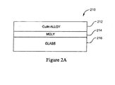
- a Cu/In composite or Cu/In alloy is formed during the sputtering process, as shown in Figure 2A .
- gallium material (not shown in Figure 2 ) may be formed deposited in addition to the copper and indium material
- FIG. 2A is a simplified diagram of a composite structure 210 including a copper and indium composite film according to another embodiment of the present invention.
- the structure 210 includes a transparent substrate 216.
- substrate 216 can be a glass substrate, for example, a soda lime glass.
- a back contact comprises a metal electrode layer 214 is deposited upon substrate 216.
- the layer 214 comprises primarily a film of molybdenum material is deposited by sputtering.
- an initial film of chromium is deposited upon glass 216 before depositing the molybdenum material to provide for good adhesion of the overall structure to the substrate 210.
- the layer 212 comprises primarily a copper (and gallium) indium alloy or copper (gallium) indium composite material.
- a copper (or CuGa alloy) indium alloy material is formed from separate layers of copper (or CuGa alloy) material and indium material, which diffuse into each layer.
- the process of forming of copper indium (or CuInGa) alloy material is performed by subjecting the structure to a high temperature annealing in an environment containing gaseous selenium species.
- FIG. 3 is a simplified diagram of a furnace according to an embodiment of the present invention. This diagram is merely an example, which should not limit the scope of the claims herein.
- a furnace 300 includes a process chamber 302 and an end cap 304.
- the reaction chamber 302 is characterized by a volume of more than 200 liters.
- the furnace 300 includes a vacuum-pumping machine that comprises a turbo molecular pump 310 and a rotary pump 312.
- the vacuum-pumping machine can be implemented by way of a combination of a mechanical booster pump and a dry pump.
- the raw material gas and/or a diluting gas such as helium, nitrogen, argon, or hydrogen can be introduced in process chamber 302 via a gas injection pipe 314, if demanded by the specific applications and/or processes.
- the chamber 302 is evacuated by the turbo molecular pump 310 via the rotary pump 312 that is connected with a manifold 316 via a gate valve and a conductance valve 318.
- a heating element 306 is mounted outside the reaction chamber 302.
- the end cap 304 of the chamber is a lid with embedded temperature control elements.
- the lid is built with lamps for generating heat and cooling water pipes for actual temperature control.
- the lid also includes quartz baffles (not shown) that serves an element for controlling exchange of heat and mass (gases) between a main spatial region of the chamber 302 and a spatial region surrounding the lid.
- the furnace 300 can be used for many applications. According to an embodiment, the furnace 300 is used to apply thermal energy to various types of substrates and to introduce various types of gaseous species, among others.
- one or more glass plates or substrates are positioned vertically near the center of chamber 302.
- substrates 308 can be similar to those described in Figures 2 and 2A (e.g., Cu/In layers or composite Cu/In layer overlying a metal contact layer on a substrate). These layers placed in the process chamber in the presence of a gas containing selenium, such as hydrogen selenide H 2 Se. After annealing the material for a given period of time, the copper, indium and selenium interdiffuse and react to form a high quality copper indium diselenide (CIS) film.
- CIS copper indium diselenide
- FIG. 4 is a simplified diagram of a process for forming a copper indium diselenide layer according to an embodiment of the present invention.
- This diagram is merely an example, which should not limit the scope of the claims herein.
- One of ordinary skill in the art would recognize many other variations, modifications, and alternatives. It is also understood that the examples and embodiments described herein are for illustrative purposes only and that various modifications or changes in light thereof will be suggested to persons skilled in the art and are to be included within the spirit and purview of this process and scope of the appended claims.
- the method 400 begins at start, step 402.
- the user of the method begins at a process chamber, such as the one noted above, as well as others.
- the process chamber can be maintained at about room temperature before proceeding with the present method. But the process chamber can start temperature ramping from a temperature higher than room temperature, such as 100 °C.
- a plurality of substrates is transferred into the process chamber, step 402.
- Each of the plurality of substrates can be provided in a vertical orientation with respect to gravity.
- the plurality of substrates can be defined by a number N, where N is greater than 5.
- the plurality of substrates can comprise 5 or more individual substrates.
- the plurality of substrates can comprise 40 or more individual substrates.
- each substrate can have a dimension of 65 cm x 165 cm or smaller. But it is understood that other dimensions are possible.
- Each of the substrates is maintained in substantially a planar configuration free from warp or damage.
- the gravitational force could cause the substrates to sag and warp unless they are placed on a supporting structure such as shelves. This occurs when the substrate material reaches a softening temperature, compromising the structural integrity of the substrate.
- glass substrates particular soda lime glass substrates, begin to soften at 480 °C.
- the substrates are also separate from one another according to a predetermined spacing to ensure even heating and reactions with gaseous species that are to be introduced to the furnace.
- gaseous species including a selenide species, and/or a carrier gas, are introduced into the process chamber in step 406.
- the gaseous species includes at least H 2 Se and nitrogen.
- the gaseous species other types of chemically inert gas, such as helium, argon, etc.
- the substrates are placed in the presence of a gas containing selenium, such as H 2 Se.
- step 408 The furnace is then heated up to a second temperature ranging from about 350 °C to 450 °C in step 408.
- the transfer of thermal energy for the purpose of heating the process chamber can be done by heating elements, heating coils, and the like.
- step 408 at least starts the formation of a copper indium diselenide film by reactions between the gaseous species and the copper and indium composite (or layered) structure on each of the substrates.
- separate layers of copper and indium material are diffused into each other to corm a single layer of copper indium alloy material.
- the second temperature is maintained for 10 to 90 minutes at the heat treatment interval between 350 °C and 450 °C, step 410.
- the second temperature range can be from 390 °C to 410 °C.
- the period of time for maintaining the temperature at step 410 is provided to allow formation of the CIS film material.
- the pressure inside the furnace may increase as well.
- a pressure release valve is used to keep the pressure within the furnace at approximately 650 torr.
- step 412 As the temperature is maintained at the second temperature (step 410) or at least when the temperature above certain threshold, the removal of the residual selenide species begins, in step 412.
- a vacuum is formed in the process chamber through a vacuum pump, in step 414.
- a sulfide species is introduced, in step 416.
- the residual selenide removal process may continue until the process chamber is in vacuum configuration.
- a second temperature ramp up process is initiated, step 418.
- an optional step may include waiting before the temperature is ramped up to allow the temperature uniformity to improve for all substrates in the main spatial region of the chamber.
- the sulfide species is introduced with nitrogen, which functions as a carrier gas occupying approximately 70 to 75% of furnace.
- the temperature of the furnace is increased to a third temperature ranging from about 500 °C to 525 °C.
- the third temperature is calibrated for reaction between the sulfide species and the substrates in furnace.
- step 420 temperature is maintained at the third temperature for a period of time until the formation of the copper indium diselenide CIS (or CIGS if gallium is included) layer is completed.
- the step is set up for the purpose of extracting out one or more selenium species from the copper indium diselenide film in the ambient of the furnace comprising the sulfur species. It is to be appreciated that a predetermined amount of selenium are removed. In a specific embodiment, approximately 5% of the selenium is removed from the CIS film and is replaced by about 5% of sulfur. According to an embodiment, a complete reaction between the selenium with the CIS film is desired. After the removal of residual selenium, a controlled temperature ramp down process is initiated, in step 422.
- the furnace is cooled to the first temperature of about room temperature, and the remaining gaseous species are removed from the furnace, in step 424.
- the gaseous species are removed by a vacuum pumping machine.
- the temperature sequence described above can be illustrated in the temperature profile in Figure 5 .
- step 420 additional steps may be performed depending on the desired end product. For example, if a CIS or CIGS type of thin-film solar cell is desired, additional processes are provided to provide additional structures, such as a transparent layer of material such as ZnO overlaying the CIS layer.
- FIG. 5 is a simplified diagram of a temperature profile of the furnace according to an embodiment of the present invention. This diagram is merely an example, which should not limit the scope of the claims herein.
- the temperature profile further details the temperature ramping process in the above-described method outline ( Figure 4 ) and specification.
- An optimized temperature profile ( Figure 5 ) is provided to illustrate a heating process according to an embodiment of the present invention.
- the process chamber is configured to include independently controlled temperature zones with heater elements properly disposed near the corresponding zones. This enables the derivation of the optimized temperature profile.
- the optimized profile regulates the process chamber in order to prevent the warping of large substrates at high temperatures. If the temperature is ramped up too high too quickly, warping or damage may occur due to the softening of glass.
- the total amount of thermal energy is determined in consideration of total thermal budget available to the substrates and to maintain the uniformity and structure integrity of the glass substrate. For example, by periodically controlling the temperature of the heating process in steps, the substrate stays at a level of stabilization and relaxing in which the requisite structure integrity is maintained. As explained above, material such as glass tends to deform at a temperature of 480 °C or higher, and thus caution is exercised to avoid prolong exposure of substrate at high temperatures. Referring to Figure 5 , while the ambience of a process chamber is maintained with a gaseous species including a selenide species and a carrier gas, a plurality of substrates is put into the furnace.
- a gaseous species including a selenide species and a carrier gas
- the plurality of substrates is provided in a vertical orientation with respect to a direction of gravity, with the plurality of substrates being defined by a number N, where N is greater than 5. In certain implementation, the number N is greater than 40.
- the substrates include glass substrates, such as soda lime glass.
- the furnace starts the process with a first temperature of about 30 °C (i.e., around room temperature). The furnace of course can start with a higher temperature, such as 100 °C. The furnace is then heated up to a second temperature ranging from about 350 °C to 450 °C.
- the second temperature is maintained for 10 to 90 minutes at the heat treatment interval between 350 °C to 450 °C.
- the size of glass substrate can be 65 cm x 165 cm or smaller.
- a challenge in processing large substrate is the warping of the substrate at high temperatures. If the temperature is ramped up directly to T3, warping or damage may occur.
- all substrates are loaded in a substrate holder or boat that sets them in substantially a planar configuration free of warp or damage.
- each substrate is disposed in the boat in substantially vertical direction relative to gravity and has a predetermined spacing from its nearest neighbor. As shown in Figure 5 , the slope of ramping up from T2 to T3 is calibrated to reduce and/or eliminate the risk of damaging the substrate.
- the substrate can relax and stabilize.
- the maintaining time at this interval is set up according to the purpose of at least initiating formation of the copper indium diselenide film from the copper and indium composite structure on each of the substrates.
- the ambient of the furnace is changed such that the selenide species is removed and a sulfide species is introduced.
- a second temperature ramp up process is initiated. There can be a delay in the ramp of furnace temperature in order to improve substrate temperature uniformity. Then, the temperature of the furnace is increased to a third temperature ranging from about 500 °C to 525 °C.
- the temperature of the furnace is maintained for 10 to 60 minutes at the heat treatment interval between 500 °C and 525 °C.
- the time interval with the temperature in a plateau in an ambient comprising a sulfur species, e.g., hydrogen sulfide gas, is set up for the purpose of extracting out one or more selenium species from the copper indium diselenide film.
- the residual selenide species can be thermally cranked or decomposed to elemental selenium particles, which can be carried away by a convective current from relative hot main spatial region of the chamber to a relative cold region such as the end cap region.
- an exchange reaction occurs to replace sulfur species for the selenium species in the film overlying the substrate.
- a predetermined amount e.g., 5 to 10%
- selenium can be extracted to provide a proper amount of selenium concentration within the CIS film.
- a controlled temperature ramp-down process is initiated, as the furnace is then cooled to the first temperature of about room temperature.
- the cooling process is specifically calibrated. As a result of this process, the copper, indium, and selenium interdiffuse and react to form a high quality copper indium diselenide film.
- FIG. 5A is a simplified diagram of a temperature profile of the furnace according to an embodiment of the present invention. This diagram is merely an example, which should not limit the scope of the claims herein.
- the temperature profile further details the temperature ramping process in the above-described method outline ( Figure 4 ) and specification.
- An optimized temperature profile ( Figure 5A ) is provided to illustrate a heating process according to an embodiment of the present invention.
- T1 is approximately set at room temperature. But it can be set as high as 100 °C.
- substrates are loaded into a furnace. Air is pumped out (e.g., by vacuum device) from the furnace, and H 2 Se and N 2 gas species are introduced into the furnace. For example, these gas species are introduced to the furnace so that at pressure of approximate 650 torr is reached.
- the rate of temperature ramping up is optimized to allow the relative uniform reaction between selenium and copper and indium (and possibly with addition of gallium).
- the T2 temperature is approximately between 350°C and 450 °C.
- the furnace stays at the T2 temperature for about 10 to 60 minutes.
- the time staying at the T2 temperature is to allow for reaction between selenium and copper indium material.
- separate layers of copper and indium material form copper indium alloy while reacting with selenium material.
- CIS and/or CIGS material is formed at T2.
- the pressure inside the furnace is controlled to sustain a relative uniform pressure level of approximate 650 torr.
- a gas escape valve is used to release gases when the furnace heat up, where pressure increases due to gas expansion at high temperature.
- the sulfide gas along with certain inert gases (e.g., nitrogen, argon, helium, etc.) is introduced to the furnace, and the temperature inside the furnace increases from T2 to T3.
- certain inert gases e.g., nitrogen, argon, helium, etc.
- T3 is approximately 500 °C to 550 °C.
- the temperature stays at T3 to allow the sulfide gas to interact with the CIGS and/or CIS material.
- the sulfur replaces approximately 3 to 10% of the selenium material from the CIGS and/or CIS material.
- the furnace is cools down in the ambient of sulfide gas which is removed at last.
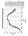
- Figure 7 shows exemplary furnace temperature profiles measured by in-situ thermal couples according to an embodiment of the present invention.
- This diagram is merely an example, which should not limit the scope of the claims herein.
- a large furnace is chosen to be the process chamber where a plurality of substrates has been loaded.
- Temperature sensors are pre-installed for monitoring all substrates on bottom, middle, and top regions.
- Figure 7 just shows the measured temperature profile during an actual processing run. It schematically illustrates realization of the temperature profile preset in Figure 5 or Figure 5A .
- FIG. 7 shows exemplary furnace temperature profiles measured by in-situ thermal couples according to an embodiment of the present invention.
- This diagram is merely an example, which should not limit the scope of the claims herein.
- a large furnace is chosen to be the process chamber where a plurality of substrates has been loaded.
- Temperature sensors are pre-installed for monitoring all substrates on bottom, middle, and top regions.
- Figure 7 just shows the measured temperature profile during an actual processing run. It schematic
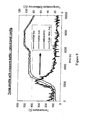
- the furnace temperature profile is controlled by adjusting the heaters surrounding the process chamber. Additionally, depending on the internal structural design and substrate configuration when loaded in the substrate holder or boat, the temperature distribution may not be plainly uniform. In fact, several temperature zones can be identified through an experiment. Therefore, the temperature profile set point for corresponding zones can be separately controlled in order to achieve an actual temperature profile with improved uniformity.
- Figure 8 just shows exemplary temperature profile set points at various zones in a furnace according to an embodiment of the present invention.
- identifying various temperature zones in the furnace for setting independent temperature control is one method.
- Other methods of improving temperature uniformity include designing proper internal structural arrangement and substrate loading configuration. For example, adding certain baffles inside the furnace inner surface can partially isolate main processing zone for achieving better temperature uniformity and controlling the internal convective flow. Adding temperature control elements to an end cap (or lid) so that it can act as a "cryopump" inside the process chamber for reduce contamination and enhance chemistry control of the reactive annealing of the film on substrate.
- Figure 9 shows exemplary furnace temperature profile and substrate temperature uniformity according to an embodiment of the present invention.
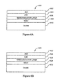
- FIG. 6 is a simplified diagram of a thin film copper indium diselenide device according to an embodiment of the present invention.
- structure 600 is supported on a glass substrate 610.
- the glass substrate comprises soda lime glass, which is about 1 to 3 millimeters thick.
- a back contact including a metal layer 608 is deposited upon substrate 610.
- layer 608 comprises primarily a film of molybdenum which has been deposited by sputtering.
- the first active region of the structure 600 comprises a semiconductor layer 606.
- the semiconductor layer includes p-type copper indium diselenide (CIS) material.
- CIS copper indium diselenide
- the second active portion of the structure 600 comprises layers 604 and 602 of n-type semiconductor material, such as CdS or ZnO.
- CdS and/or ZnO layers function as a winder layers.
- ZnO is shown overlaying the CdS layer.
- the ZnO layer 602 overlays another ZnO layer that is characterized by a different resistivity.
- a photovoltaic cell, or solar cell, such as device 600 described above, is configured as a large-area p-n junction.
- the photons may be reflected, pass through the transparent electrode layer, or become absorbed.
- the semiconductor layer absorbs the energy causing electron-hole pairs to be created.
- a photon needs to have greater energy than that of the band gap in order to excite an electron from the valence band into the conduction band. This allows the electrons to flow through the material to produce a current.
- the complementary positive charges, or holes flow in the direction opposite of the electrons in a photovoltaic cell.
- a solar panel having many photovoltaic cells can convert solar energy into direct current electricity.
- CIS copper indium diselenide
- the present invention provides methods for making CIS-based and/or CIGS-based solar cells on a large glass substrate for a solar panel.
- the device structure described in Figure 6 can be patterned into individual solar cells on the glass substrate and interconnected to form the solar panel.
- the present invention thus provides a cost-effective method for making thin film solar cell panel.
- FIG. 10 shows an exemplary cell open-circuit voltage distribution from ten substrates in a furnace according to an embodiment of the present invention.
- This diagram is merely an example, which should not limit the scope of the claims herein.
- 10 soda lime glass substrates have been loaded into a furnace described before and been carried out a series of large scale selenization and sufurization processes for forming a CIS based photovoltaic absorber film.
- a key parameter, cell open-circuit voltages Voc is measured around 0.5 V for cells made from those films out of the 10 substrates.
- Figure 10 just shows that the Voc value distribution has achieved desired uniformity across all substrates in this large scale production process.
Landscapes
- Chemical & Material Sciences (AREA)
- Chemical Kinetics & Catalysis (AREA)
- Engineering & Computer Science (AREA)
- Materials Engineering (AREA)
- Mechanical Engineering (AREA)
- Metallurgy (AREA)
- Organic Chemistry (AREA)
- Photovoltaic Devices (AREA)
- Physical Vapour Deposition (AREA)
Applications Claiming Priority (1)
| Application Number | Priority Date | Filing Date | Title |
|---|---|---|---|
| US12/568,641 US7910399B1 (en) | 2008-09-30 | 2009-09-28 | Thermal management and method for large scale processing of CIS and/or CIGS based thin films overlying glass substrates |
Publications (1)
| Publication Number | Publication Date |
|---|---|
| EP2319954A1 true EP2319954A1 (fr) | 2011-05-11 |
Family
ID=43708937
Family Applications (1)
| Application Number | Title | Priority Date | Filing Date |
|---|---|---|---|
| EP10011072A Withdrawn EP2319954A1 (fr) | 2009-09-28 | 2010-09-28 | Procédé pour la fabrication d'une couche mince de CIS et/ou de CIGS sur des substrats de verre |
Country Status (3)
| Country | Link |
|---|---|
| EP (1) | EP2319954A1 (fr) |
| CN (1) | CN102034895B (fr) |
| TW (1) | TWI488313B (fr) |
Cited By (3)
| Publication number | Priority date | Publication date | Assignee | Title |
|---|---|---|---|---|
| TWI460139B (zh) * | 2011-07-29 | 2014-11-11 | Young Optics Inc | 玻璃製品的製作方法與製作系統及電子裝置 |
| TWI475713B (zh) * | 2012-05-16 | 2015-03-01 | Tangteck Equipment Inc | 薄膜太陽能電池之製造方法 |
| CN110957393A (zh) * | 2019-12-13 | 2020-04-03 | 深圳先进技术研究院 | 薄膜太阳能电池的光吸收层的制备方法 |
Families Citing this family (4)
| Publication number | Priority date | Publication date | Assignee | Title |
|---|---|---|---|---|
| CN103779439B (zh) * | 2012-10-22 | 2016-09-21 | 中物院成都科学技术发展中心 | 一种铜铟镓硒薄膜预制层及其制备方法 |
| CN105336800B (zh) * | 2015-10-28 | 2017-03-29 | 厦门神科太阳能有限公司 | Cigs基薄膜太阳能电池光吸收层的制备方法 |
| US10483101B2 (en) | 2016-06-30 | 2019-11-19 | Corning Incorporated | Glass-based article with engineered stress distribution and method of making same |
| TWI763684B (zh) * | 2017-07-10 | 2022-05-11 | 美商康寧公司 | 具有經設計之應力分佈的以玻璃為基礎之製品及其製作方法 |
Citations (6)
| Publication number | Priority date | Publication date | Assignee | Title |
|---|---|---|---|---|
| US4611091A (en) | 1984-12-06 | 1986-09-09 | Atlantic Richfield Company | CuInSe2 thin film solar cell with thin CdS and transparent window layer |
| US4612411A (en) | 1985-06-04 | 1986-09-16 | Atlantic Richfield Company | Thin film solar cell with ZnO window layer |
| WO2007058702A1 (fr) * | 2005-11-18 | 2007-05-24 | Daystar Technologies, Inc. | Procedes et appareil de traitement de piece de fabrication avec un element vaporeux |
| EP1833097A1 (fr) * | 2004-12-28 | 2007-09-12 | Showa Shell Sekiyu Kabushiki Kaisha | Procede d'elaboration d'une couche d'absorption de lumiere dans une batterie solairea film mince a base cis |
| DE102008008518A1 (de) * | 2008-02-11 | 2009-08-13 | Avancis Gmbh & Co. Kg | Verfahren und Vorrichtung zur Herstellung von Solarzellen und -modulen, insbesondere Dünnschicht-Solarmodulen |
| WO2010060646A1 (fr) * | 2008-11-28 | 2010-06-03 | Volker Probst | Procédé de fabrication de couches semi-conductrices ou de substrats revêtus, traités par du sélénium et/ou du soufre élémentaire, en particulier de substrats bidimensionnels |
Family Cites Families (3)
| Publication number | Priority date | Publication date | Assignee | Title |
|---|---|---|---|---|
| EP1521308A1 (fr) * | 2003-10-02 | 2005-04-06 | Scheuten Glasgroep | Composant semiconducteur sphérique ou granulaire utilisé pour des cellules solaires et son procédé de fabrication; procédé de fabrication d'une cellule solaire avec ce composant semiconducteur et cellule solaire |
| CN100413097C (zh) * | 2005-06-03 | 2008-08-20 | 清华大学 | 铜铟镓硒或铜铟镓硫或铜铟镓硒硫薄膜太阳能电池吸收层的制备方法 |
| CN101383389A (zh) * | 2008-10-07 | 2009-03-11 | 苏州富能技术有限公司 | 铜铟镓硒硫或铜铟镓硒或铜铟镓硫薄膜太阳能电池吸收层的制备方法及镀膜设备 |
-
2010
- 2010-09-28 CN CN201010503956.5A patent/CN102034895B/zh not_active Expired - Fee Related
- 2010-09-28 TW TW099132907A patent/TWI488313B/zh not_active IP Right Cessation
- 2010-09-28 EP EP10011072A patent/EP2319954A1/fr not_active Withdrawn
Patent Citations (6)
| Publication number | Priority date | Publication date | Assignee | Title |
|---|---|---|---|---|
| US4611091A (en) | 1984-12-06 | 1986-09-09 | Atlantic Richfield Company | CuInSe2 thin film solar cell with thin CdS and transparent window layer |
| US4612411A (en) | 1985-06-04 | 1986-09-16 | Atlantic Richfield Company | Thin film solar cell with ZnO window layer |
| EP1833097A1 (fr) * | 2004-12-28 | 2007-09-12 | Showa Shell Sekiyu Kabushiki Kaisha | Procede d'elaboration d'une couche d'absorption de lumiere dans une batterie solairea film mince a base cis |
| WO2007058702A1 (fr) * | 2005-11-18 | 2007-05-24 | Daystar Technologies, Inc. | Procedes et appareil de traitement de piece de fabrication avec un element vaporeux |
| DE102008008518A1 (de) * | 2008-02-11 | 2009-08-13 | Avancis Gmbh & Co. Kg | Verfahren und Vorrichtung zur Herstellung von Solarzellen und -modulen, insbesondere Dünnschicht-Solarmodulen |
| WO2010060646A1 (fr) * | 2008-11-28 | 2010-06-03 | Volker Probst | Procédé de fabrication de couches semi-conductrices ou de substrats revêtus, traités par du sélénium et/ou du soufre élémentaire, en particulier de substrats bidimensionnels |
Cited By (4)
| Publication number | Priority date | Publication date | Assignee | Title |
|---|---|---|---|---|
| TWI460139B (zh) * | 2011-07-29 | 2014-11-11 | Young Optics Inc | 玻璃製品的製作方法與製作系統及電子裝置 |
| TWI475713B (zh) * | 2012-05-16 | 2015-03-01 | Tangteck Equipment Inc | 薄膜太陽能電池之製造方法 |
| CN110957393A (zh) * | 2019-12-13 | 2020-04-03 | 深圳先进技术研究院 | 薄膜太阳能电池的光吸收层的制备方法 |
| CN110957393B (zh) * | 2019-12-13 | 2022-07-19 | 深圳先进技术研究院 | 薄膜太阳能电池的光吸收层的制备方法 |
Also Published As
| Publication number | Publication date |
|---|---|
| CN102034895A (zh) | 2011-04-27 |
| TW201123470A (en) | 2011-07-01 |
| TWI488313B (zh) | 2015-06-11 |
| CN102034895B (zh) | 2016-02-03 |
Similar Documents
| Publication | Publication Date | Title |
|---|---|---|
| US7955891B2 (en) | Thermal management and method for large scale processing of CIS and /or CIGS based thin films overlying glass substrates | |
| US8377736B2 (en) | System and method for transferring substrates in large scale processing of CIGS and/or CIS devices | |
| US8053274B2 (en) | Self cleaning large scale method and furnace system for selenization of thin film photovoltaic materials | |
| CN102034895B (zh) | 用于大规模处理覆盖玻璃基板的基于cis和/或cigs的薄膜的热管理和方法 | |
| US8008198B1 (en) | Large scale method and furnace system for selenization of thin film photovoltaic materials | |
| JP2012007194A (ja) | 成膜装置および光電変換素子の製造方法 | |
| WO2012090506A1 (fr) | Appareil de dépôt de film et procédé de fabrication d'un élément de conversion photoélectrique | |
| KR101299189B1 (ko) | 멀티 스테이지공정을 이용한 대면적 유리기판 cigs 박막의 연속 제조용 인라인 장비시스템과 대면적 유리기판 cigs 박막의 제조방법 | |
| US8372684B1 (en) | Method and system for selenization in fabricating CIGS/CIS solar cells | |
| US9076917B2 (en) | Method of manufacturing photovoltaic cell | |
| CN102034896B (zh) | 利用自清洁熔炉制造铜铟二硒化物半导体膜的方法 | |
| WO2011135420A1 (fr) | Procédé destiné à la production d'une couche de semi-conducteur composite |
Legal Events
| Date | Code | Title | Description |
|---|---|---|---|
| PUAI | Public reference made under article 153(3) epc to a published international application that has entered the european phase |
Free format text: ORIGINAL CODE: 0009012 |
|
| AK | Designated contracting states |
Kind code of ref document: A1 Designated state(s): AL AT BE BG CH CY CZ DE DK EE ES FI FR GB GR HR HU IE IS IT LI LT LU LV MC MK MT NL NO PL PT RO SE SI SK SM TR |
|
| AX | Request for extension of the european patent |
Extension state: BA ME RS |
|
| 17P | Request for examination filed |
Effective date: 20111110 |
|
| 17Q | First examination report despatched |
Effective date: 20151211 |
|
| STAA | Information on the status of an ep patent application or granted ep patent |
Free format text: STATUS: THE APPLICATION IS DEEMED TO BE WITHDRAWN |
|
| 18D | Application deemed to be withdrawn |
Effective date: 20160622 |