EP2320480A2 - Couche pour photovoltaïques à couche mince et cellule solaire fabriquée à partir de la couche - Google Patents
Couche pour photovoltaïques à couche mince et cellule solaire fabriquée à partir de la couche Download PDFInfo
- Publication number
- EP2320480A2 EP2320480A2 EP10189301A EP10189301A EP2320480A2 EP 2320480 A2 EP2320480 A2 EP 2320480A2 EP 10189301 A EP10189301 A EP 10189301A EP 10189301 A EP10189301 A EP 10189301A EP 2320480 A2 EP2320480 A2 EP 2320480A2
- Authority
- EP
- European Patent Office
- Prior art keywords
- layer
- absorber layer
- absorber
- photovoltaic device
- electron volts
- Prior art date
- Legal status (The legal status is an assumption and is not a legal conclusion. Google has not performed a legal analysis and makes no representation as to the accuracy of the status listed.)
- Withdrawn
Links
- 239000010409 thin film Substances 0.000 title 1
- 239000006096 absorbing agent Substances 0.000 claims abstract description 190
- 239000004065 semiconductor Substances 0.000 claims abstract description 51
- 238000000034 method Methods 0.000 claims abstract description 42
- 229910052710 silicon Inorganic materials 0.000 claims abstract description 37
- 239000010703 silicon Substances 0.000 claims abstract description 37
- MARUHZGHZWCEQU-UHFFFAOYSA-N 5-phenyl-2h-tetrazole Chemical compound C1=CC=CC=C1C1=NNN=N1 MARUHZGHZWCEQU-UHFFFAOYSA-N 0.000 claims description 59
- 229910021417 amorphous silicon Inorganic materials 0.000 claims description 22
- 229910052714 tellurium Inorganic materials 0.000 claims description 17
- PORWMNRCUJJQNO-UHFFFAOYSA-N tellurium atom Chemical compound [Te] PORWMNRCUJJQNO-UHFFFAOYSA-N 0.000 claims description 15
- HMDDXIMCDZRSNE-UHFFFAOYSA-N [C].[Si] Chemical compound [C].[Si] HMDDXIMCDZRSNE-UHFFFAOYSA-N 0.000 claims description 5
- XUIMIQQOPSSXEZ-UHFFFAOYSA-N Silicon Chemical compound [Si] XUIMIQQOPSSXEZ-UHFFFAOYSA-N 0.000 description 29
- YKYOUMDCQGMQQO-UHFFFAOYSA-L cadmium dichloride Chemical compound Cl[Cd]Cl YKYOUMDCQGMQQO-UHFFFAOYSA-L 0.000 description 21
- 239000000463 material Substances 0.000 description 16
- 239000000758 substrate Substances 0.000 description 13
- 229910052751 metal Inorganic materials 0.000 description 11
- 239000002184 metal Substances 0.000 description 11
- 238000000151 deposition Methods 0.000 description 10
- 239000010949 copper Substances 0.000 description 9
- RYGMFSIKBFXOCR-UHFFFAOYSA-N Copper Chemical compound [Cu] RYGMFSIKBFXOCR-UHFFFAOYSA-N 0.000 description 7
- 230000004888 barrier function Effects 0.000 description 7
- 238000002202 sandwich sublimation Methods 0.000 description 7
- 229910052802 copper Inorganic materials 0.000 description 6
- 238000005530 etching Methods 0.000 description 6
- 238000004519 manufacturing process Methods 0.000 description 6
- 238000000623 plasma-assisted chemical vapour deposition Methods 0.000 description 6
- SKJCKYVIQGBWTN-UHFFFAOYSA-N (4-hydroxyphenyl) methanesulfonate Chemical compound CS(=O)(=O)OC1=CC=C(O)C=C1 SKJCKYVIQGBWTN-UHFFFAOYSA-N 0.000 description 5
- WUPHOULIZUERAE-UHFFFAOYSA-N 3-(oxolan-2-yl)propanoic acid Chemical compound OC(=O)CCC1CCCO1 WUPHOULIZUERAE-UHFFFAOYSA-N 0.000 description 5
- 229910052980 cadmium sulfide Inorganic materials 0.000 description 5
- 230000008021 deposition Effects 0.000 description 5
- PCHJSUWPFVWCPO-UHFFFAOYSA-N gold Chemical compound [Au] PCHJSUWPFVWCPO-UHFFFAOYSA-N 0.000 description 5
- 150000002739 metals Chemical class 0.000 description 5
- ZOXJGFHDIHLPTG-UHFFFAOYSA-N Boron Chemical compound [B] ZOXJGFHDIHLPTG-UHFFFAOYSA-N 0.000 description 4
- OKTJSMMVPCPJKN-UHFFFAOYSA-N Carbon Chemical compound [C] OKTJSMMVPCPJKN-UHFFFAOYSA-N 0.000 description 4
- VEXZGXHMUGYJMC-UHFFFAOYSA-N Hydrochloric acid Chemical compound Cl VEXZGXHMUGYJMC-UHFFFAOYSA-N 0.000 description 4
- PXHVJJICTQNCMI-UHFFFAOYSA-N Nickel Chemical compound [Ni] PXHVJJICTQNCMI-UHFFFAOYSA-N 0.000 description 4
- XLOMVQKBTHCTTD-UHFFFAOYSA-N Zinc monoxide Chemical compound [Zn]=O XLOMVQKBTHCTTD-UHFFFAOYSA-N 0.000 description 4
- LEVVHYCKPQWKOP-UHFFFAOYSA-N [Si].[Ge] Chemical compound [Si].[Ge] LEVVHYCKPQWKOP-UHFFFAOYSA-N 0.000 description 4
- 238000010521 absorption reaction Methods 0.000 description 4
- 229910052796 boron Inorganic materials 0.000 description 4
- 229910052799 carbon Inorganic materials 0.000 description 4
- 229910052737 gold Inorganic materials 0.000 description 4
- 239000010931 gold Substances 0.000 description 4
- 238000012545 processing Methods 0.000 description 4
- WXRGABKACDFXMG-UHFFFAOYSA-N trimethylborane Chemical compound CB(C)C WXRGABKACDFXMG-UHFFFAOYSA-N 0.000 description 4
- 239000011701 zinc Substances 0.000 description 4
- UFHFLCQGNIYNRP-UHFFFAOYSA-N Hydrogen Chemical compound [H][H] UFHFLCQGNIYNRP-UHFFFAOYSA-N 0.000 description 3
- 229910000577 Silicon-germanium Inorganic materials 0.000 description 3
- HCHKCACWOHOZIP-UHFFFAOYSA-N Zinc Chemical compound [Zn] HCHKCACWOHOZIP-UHFFFAOYSA-N 0.000 description 3
- 229910052782 aluminium Inorganic materials 0.000 description 3
- XAGFODPZIPBFFR-UHFFFAOYSA-N aluminium Chemical compound [Al] XAGFODPZIPBFFR-UHFFFAOYSA-N 0.000 description 3
- BDOSMKKIYDKNTQ-UHFFFAOYSA-N cadmium atom Chemical group [Cd] BDOSMKKIYDKNTQ-UHFFFAOYSA-N 0.000 description 3
- 239000000969 carrier Substances 0.000 description 3
- 238000006243 chemical reaction Methods 0.000 description 3
- 229910021419 crystalline silicon Inorganic materials 0.000 description 3
- 230000005611 electricity Effects 0.000 description 3
- 239000011521 glass Substances 0.000 description 3
- 229910052739 hydrogen Inorganic materials 0.000 description 3
- 239000001257 hydrogen Substances 0.000 description 3
- 239000012535 impurity Substances 0.000 description 3
- VNWKTOKETHGBQD-UHFFFAOYSA-N methane Chemical compound C VNWKTOKETHGBQD-UHFFFAOYSA-N 0.000 description 3
- XSOKHXFFCGXDJZ-UHFFFAOYSA-N telluride(2-) Chemical compound [Te-2] XSOKHXFFCGXDJZ-UHFFFAOYSA-N 0.000 description 3
- 229910052725 zinc Inorganic materials 0.000 description 3
- PFNQVRZLDWYSCW-UHFFFAOYSA-N (fluoren-9-ylideneamino) n-naphthalen-1-ylcarbamate Chemical compound C12=CC=CC=C2C2=CC=CC=C2C1=NOC(=O)NC1=CC=CC2=CC=CC=C12 PFNQVRZLDWYSCW-UHFFFAOYSA-N 0.000 description 2
- XKRFYHLGVUSROY-UHFFFAOYSA-N Argon Chemical compound [Ar] XKRFYHLGVUSROY-UHFFFAOYSA-N 0.000 description 2
- JBRZTFJDHDCESZ-UHFFFAOYSA-N AsGa Chemical compound [As]#[Ga] JBRZTFJDHDCESZ-UHFFFAOYSA-N 0.000 description 2
- VYZAMTAEIAYCRO-UHFFFAOYSA-N Chromium Chemical compound [Cr] VYZAMTAEIAYCRO-UHFFFAOYSA-N 0.000 description 2
- ZOKXTWBITQBERF-UHFFFAOYSA-N Molybdenum Chemical compound [Mo] ZOKXTWBITQBERF-UHFFFAOYSA-N 0.000 description 2
- BLRPTPMANUNPDV-UHFFFAOYSA-N Silane Chemical compound [SiH4] BLRPTPMANUNPDV-UHFFFAOYSA-N 0.000 description 2
- VYPSYNLAJGMNEJ-UHFFFAOYSA-N Silicium dioxide Chemical compound O=[Si]=O VYPSYNLAJGMNEJ-UHFFFAOYSA-N 0.000 description 2
- 239000005083 Zinc sulfide Substances 0.000 description 2
- QDOSJNSYIUHXQG-UHFFFAOYSA-N [Mn].[Cd] Chemical compound [Mn].[Cd] QDOSJNSYIUHXQG-UHFFFAOYSA-N 0.000 description 2
- 230000008901 benefit Effects 0.000 description 2
- 229910052793 cadmium Inorganic materials 0.000 description 2
- WZGKIRHYWDCEKP-UHFFFAOYSA-N cadmium magnesium Chemical compound [Mg].[Cd] WZGKIRHYWDCEKP-UHFFFAOYSA-N 0.000 description 2
- CJOBVZJTOIVNNF-UHFFFAOYSA-N cadmium sulfide Chemical compound [Cd]=S CJOBVZJTOIVNNF-UHFFFAOYSA-N 0.000 description 2
- QWUZMTJBRUASOW-UHFFFAOYSA-N cadmium tellanylidenezinc Chemical compound [Zn].[Cd].[Te] QWUZMTJBRUASOW-UHFFFAOYSA-N 0.000 description 2
- 239000002800 charge carrier Substances 0.000 description 2
- 229910052804 chromium Inorganic materials 0.000 description 2
- 239000011651 chromium Substances 0.000 description 2
- 238000013461 design Methods 0.000 description 2
- 238000011161 development Methods 0.000 description 2
- 238000004070 electrodeposition Methods 0.000 description 2
- 229910052732 germanium Inorganic materials 0.000 description 2
- GNPVGFCGXDBREM-UHFFFAOYSA-N germanium atom Chemical compound [Ge] GNPVGFCGXDBREM-UHFFFAOYSA-N 0.000 description 2
- AKUCEXGLFUSJCD-UHFFFAOYSA-N indium(3+);selenium(2-) Chemical compound [Se-2].[Se-2].[Se-2].[In+3].[In+3] AKUCEXGLFUSJCD-UHFFFAOYSA-N 0.000 description 2
- 150000002500 ions Chemical class 0.000 description 2
- 238000001755 magnetron sputter deposition Methods 0.000 description 2
- 229910021424 microcrystalline silicon Inorganic materials 0.000 description 2
- 238000012986 modification Methods 0.000 description 2
- 230000004048 modification Effects 0.000 description 2
- 229910052750 molybdenum Inorganic materials 0.000 description 2
- 239000011733 molybdenum Substances 0.000 description 2
- 229910052759 nickel Inorganic materials 0.000 description 2
- 230000003287 optical effect Effects 0.000 description 2
- 238000005240 physical vapour deposition Methods 0.000 description 2
- BASFCYQUMIYNBI-UHFFFAOYSA-N platinum Chemical compound [Pt] BASFCYQUMIYNBI-UHFFFAOYSA-N 0.000 description 2
- 238000005215 recombination Methods 0.000 description 2
- 230000006798 recombination Effects 0.000 description 2
- 239000007787 solid Substances 0.000 description 2
- 239000011787 zinc oxide Substances 0.000 description 2
- 229910052984 zinc sulfide Inorganic materials 0.000 description 2
- GTIUFDICMGTSPM-UHFFFAOYSA-N 12044-54-1 Chemical compound [Te]=[As][Te][As]=[Te] GTIUFDICMGTSPM-UHFFFAOYSA-N 0.000 description 1
- 229910001218 Gallium arsenide Inorganic materials 0.000 description 1
- 229910004262 HgTe Inorganic materials 0.000 description 1
- 239000000853 adhesive Substances 0.000 description 1
- 230000001070 adhesive effect Effects 0.000 description 1
- 150000001450 anions Chemical class 0.000 description 1
- 239000006117 anti-reflective coating Substances 0.000 description 1
- 238000013459 approach Methods 0.000 description 1
- 229910052786 argon Inorganic materials 0.000 description 1
- 230000015572 biosynthetic process Effects 0.000 description 1
- PLZFHNWCKKPCMI-UHFFFAOYSA-N cadmium copper Chemical compound [Cu].[Cd] PLZFHNWCKKPCMI-UHFFFAOYSA-N 0.000 description 1
- CXKCTMHTOKXKQT-UHFFFAOYSA-N cadmium oxide Inorganic materials [Cd]=O CXKCTMHTOKXKQT-UHFFFAOYSA-N 0.000 description 1
- AQCDIIAORKRFCD-UHFFFAOYSA-N cadmium selenide Chemical compound [Cd]=[Se] AQCDIIAORKRFCD-UHFFFAOYSA-N 0.000 description 1
- CFEAAQFZALKQPA-UHFFFAOYSA-N cadmium(2+);oxygen(2-) Chemical compound [O-2].[Cd+2] CFEAAQFZALKQPA-UHFFFAOYSA-N 0.000 description 1
- BEQNOZDXPONEMR-UHFFFAOYSA-N cadmium;oxotin Chemical compound [Cd].[Sn]=O BEQNOZDXPONEMR-UHFFFAOYSA-N 0.000 description 1
- 230000015556 catabolic process Effects 0.000 description 1
- 239000012141 concentrate Substances 0.000 description 1
- 239000000356 contaminant Substances 0.000 description 1
- 238000011109 contamination Methods 0.000 description 1
- 239000013078 crystal Substances 0.000 description 1
- 238000006731 degradation reaction Methods 0.000 description 1
- 238000010586 diagram Methods 0.000 description 1
- ZOCHARZZJNPSEU-UHFFFAOYSA-N diboron Chemical compound B#B ZOCHARZZJNPSEU-UHFFFAOYSA-N 0.000 description 1
- 239000002019 doping agent Substances 0.000 description 1
- 230000005670 electromagnetic radiation Effects 0.000 description 1
- 230000007613 environmental effect Effects 0.000 description 1
- 230000005281 excited state Effects 0.000 description 1
- 239000011888 foil Substances 0.000 description 1
- 229910000078 germane Inorganic materials 0.000 description 1
- QUZPNFFHZPRKJD-UHFFFAOYSA-N germane Chemical compound [GeH4] QUZPNFFHZPRKJD-UHFFFAOYSA-N 0.000 description 1
- 229910052986 germanium hydride Inorganic materials 0.000 description 1
- 230000005283 ground state Effects 0.000 description 1
- SIXIBASSFIFHDK-UHFFFAOYSA-N indium(3+);trisulfide Chemical compound [S-2].[S-2].[S-2].[In+3].[In+3] SIXIBASSFIFHDK-UHFFFAOYSA-N 0.000 description 1
- AMGQUBHHOARCQH-UHFFFAOYSA-N indium;oxotin Chemical compound [In].[Sn]=O AMGQUBHHOARCQH-UHFFFAOYSA-N 0.000 description 1
- 238000009413 insulation Methods 0.000 description 1
- QSHDDOUJBYECFT-UHFFFAOYSA-N mercury Chemical compound [Hg] QSHDDOUJBYECFT-UHFFFAOYSA-N 0.000 description 1
- 229910052753 mercury Inorganic materials 0.000 description 1
- VCEXCCILEWFFBG-UHFFFAOYSA-N mercury telluride Chemical compound [Hg]=[Te] VCEXCCILEWFFBG-UHFFFAOYSA-N 0.000 description 1
- 239000000203 mixture Substances 0.000 description 1
- KYKLWYKWCAYAJY-UHFFFAOYSA-N oxotin;zinc Chemical compound [Zn].[Sn]=O KYKLWYKWCAYAJY-UHFFFAOYSA-N 0.000 description 1
- 229910052697 platinum Inorganic materials 0.000 description 1
- 229920000642 polymer Polymers 0.000 description 1
- 230000005855 radiation Effects 0.000 description 1
- 229910000077 silane Inorganic materials 0.000 description 1
- 239000000377 silicon dioxide Substances 0.000 description 1
- 229960001866 silicon dioxide Drugs 0.000 description 1
- 235000012239 silicon dioxide Nutrition 0.000 description 1
- 239000012686 silicon precursor Substances 0.000 description 1
- DDJAGKOCVFYQOV-UHFFFAOYSA-N tellanylideneantimony Chemical compound [Te]=[Sb] DDJAGKOCVFYQOV-UHFFFAOYSA-N 0.000 description 1
- QZCHKAUWIRYEGK-UHFFFAOYSA-N tellanylidenecopper Chemical compound [Te]=[Cu] QZCHKAUWIRYEGK-UHFFFAOYSA-N 0.000 description 1
- XOLBLPGZBRYERU-UHFFFAOYSA-N tin dioxide Chemical compound O=[Sn]=O XOLBLPGZBRYERU-UHFFFAOYSA-N 0.000 description 1
- 229910001887 tin oxide Inorganic materials 0.000 description 1
- DRDVZXDWVBGGMH-UHFFFAOYSA-N zinc;sulfide Chemical compound [S-2].[Zn+2] DRDVZXDWVBGGMH-UHFFFAOYSA-N 0.000 description 1
Images

Classifications
-
- H—ELECTRICITY
- H10—SEMICONDUCTOR DEVICES; ELECTRIC SOLID-STATE DEVICES NOT OTHERWISE PROVIDED FOR
- H10F—INORGANIC SEMICONDUCTOR DEVICES SENSITIVE TO INFRARED RADIATION, LIGHT, ELECTROMAGNETIC RADIATION OF SHORTER WAVELENGTH OR CORPUSCULAR RADIATION
- H10F77/00—Constructional details of devices covered by this subclass
- H10F77/10—Semiconductor bodies
- H10F77/12—Active materials
- H10F77/123—Active materials comprising only Group II-VI materials, e.g. CdS, ZnS or HgCdTe
-
- H—ELECTRICITY
- H10—SEMICONDUCTOR DEVICES; ELECTRIC SOLID-STATE DEVICES NOT OTHERWISE PROVIDED FOR
- H10F—INORGANIC SEMICONDUCTOR DEVICES SENSITIVE TO INFRARED RADIATION, LIGHT, ELECTROMAGNETIC RADIATION OF SHORTER WAVELENGTH OR CORPUSCULAR RADIATION
- H10F71/00—Manufacture or treatment of devices covered by this subclass
- H10F71/125—The active layers comprising only Group II-VI materials, e.g. CdS, ZnS or CdTe
- H10F71/1257—The active layers comprising only Group II-VI materials, e.g. CdS, ZnS or CdTe comprising growth substrates not made of Group II-VI materials
-
- Y—GENERAL TAGGING OF NEW TECHNOLOGICAL DEVELOPMENTS; GENERAL TAGGING OF CROSS-SECTIONAL TECHNOLOGIES SPANNING OVER SEVERAL SECTIONS OF THE IPC; TECHNICAL SUBJECTS COVERED BY FORMER USPC CROSS-REFERENCE ART COLLECTIONS [XRACs] AND DIGESTS
- Y02—TECHNOLOGIES OR APPLICATIONS FOR MITIGATION OR ADAPTATION AGAINST CLIMATE CHANGE
- Y02E—REDUCTION OF GREENHOUSE GAS [GHG] EMISSIONS, RELATED TO ENERGY GENERATION, TRANSMISSION OR DISTRIBUTION
- Y02E10/00—Energy generation through renewable energy sources
- Y02E10/50—Photovoltaic [PV] energy
Definitions
- the invention relates generally to the field of photovoltaics.
- the invention relates to a layer used in a photovoltaic device and a solar panel made therefrom.
- Solar energy is abundant in many parts of the world year around. Unfortunately, the available solar energy is not generally used efficiently to produce electricity. The cost of conventional solar cells, and electricity generated by these cells, is generally very high. For example, a typical solar cell achieves a conversion efficiency of less than 20 percent. Moreover, solar cells typically include multiple layers formed on a substrate, and thus solar cell manufacturing typically requires a significant number of processing steps. As a result, the high number of processing steps, layers, interfaces, and complexity increase the amount of time and money required to manufacture these solar cells.
- a photovoltaic device comprises an absorber layer comprising a p-type semiconductor, wherein at least one layer is disposed over the absorber layer.
- the at least one layer is a semiconductor having a higher carrier density than the carrier density of the absorber layer.
- the at least one layer comprises silicon.
- the at least one layer comprises a p+-type semiconductor.
- the absorber layer is substantially free of silicon.
- the device comprises an absorber layer, wherein the absorber layer comprises a tellurium-containing II-VI semiconductor.
- the at least one layer is disposed over the absorber layer.
- the at least one layer is a p+-type semiconductor, comprising silicon.
- the device comprises an absorber layer, wherein the absorber layer comprises a p-type tellurium-containing II-VI semiconductor.
- the at least one layer is disposed over the absorber layer.
- the at least one layer is a p+-type semiconductor, comprising silicon.
- the device comprises an absorber layer, wherein the absorber layer comprises a p-type cadmium telluride. At least one layer is disposed over the absorber layer, wherein the at least one layer comprises a p+-type hydrogenated amorphous silicon.
- the device comprises an absorber layer, wherein the absorber layer comprises a p-type cadmium telluride. At least one layer is disposed over the absorber layer, wherein the at least one layer comprises a p+-type hydrogenated amorphous-silicon carbon.
- Still yet another embodiment is a method.
- the method comprises a first step of providing an absorber layer in a photovoltaic device.
- the absorber layer is treated to increase its carrier density. Further, the absorber layer is etched to provide a stoichiometric absorber layer.
- the absorber layer comprises a p-type semiconductor.
- the absorber layer is substantially free of silicon.
- At least one layer is disposed over the absorber layer.
- the at least one layer is a semiconductor having a higher carrier density than the carrier density of the absorber layer.
- the at least one layer comprises a p+-type semiconductor.
- the at least one layer comprises silicon.
- Cadmium telluride (CdTe) based solar devices known in the art typically demonstrate relatively low power conversion efficiencies, which may be attributed to a relatively low open circuit voltage ( V oc ) in relation to the band gap of the material. Further issues with improving the cell efficiency of CdTe solar cells include the high work function of CdTe.
- the high work function of CdTe leaves a narrow choice of metals that can be employed to form an Ohmic contact with the CdTe layer.
- the metals include platinum and gold, which are not commercially viable metals for low-cost mass-production of the CdTe solar cells. However, though other metals like molybdenum, nickel, chromium, etc.
- the holes will need to tunnel through the barrier region.
- this barrier may be relatively large. It has been found that without proper treatment of the backside of the CdTe layer, the resistance with the back contact layer is significant and the fill factor of the device is reduced, thus reducing the efficiency of the device.
- One approach to improve the back-contact resistance includes increasing the carrier concentration in the regions near the contact points of the CdTe layer and the back contact layer, wherein the back contact layer is a metal layer.
- carrier concentration refers to the concentration of the holes and electrons in a material.
- higher carrier density means the concentration of the p-type charge carriers in the at least one layer formed using the p+-layer is higher than the concentration of the p-type charge carriers in the absorber layer. Creating a highly doped area with carrier density of greater than or equal to 1 x 10 17 per cubic centimeter may help in lowering the contact resistance with the back contact layer.
- One method includes treating the backside of the CdTe absorber layer that will be in contact with the back contact layer with copper or gold.
- the copper atoms or gold atoms replace the cadmium atoms in the crystal lattice creating additional acceptor states near the back contact.
- Another method includes forming a thin layer of a different phase material, such as for example mercury telluride (HgTe), zinc telluride (ZnTe), copper telluride (Cu x Te), arsenic telluride (As 2 Te 3 ), or antimony telluride (Sb 2 Te 3 ), on the backside of the CdTe layer. Valence band alignment is achieved through the anion rule.
- One method of forming such a layer includes forming a tellurium-rich layer on the backside of the CdTe layer, using the cadmium chloride (CdC1 2 ) treatment to increase the carrier density in the CdTe layer.
- a copper layer is deposited on the CdC1 2 treated CdTe layer to form a Cu x Te phase which forms the p+-type layer.
- the p + -type layers have significant drawbacks.
- gold and copper are used, both gold and copper are known to diffuse through the material, over the lifetime of the device, causing significant degradation.
- HgTe has some environmental concerns due to mercury contamination.
- Copper tellurium (Cu x Te) and zinc tellurium (ZnTe) provide a maximum charge density limited to maximum 10 18 per cubic centimeter due to the multi-crystalline nature of the films formed.
- the p+-layer formed by replacing the cadmium by copper and zinc may not have sufficiently high carrier concentration of holes meaning the concentration of holes may be below 10 18 per cubic centimeter.
- An alternative layer and method is provided herein to better overcome the differences in charge densities at the interface of the absorber layer and the at least one layer, providing a material that is compatible with absorber layer materials, such as CdTe.
- the alternative layer may be used as an interface between the absorber layer and the back contact layer with carrier densities that can equal or exceed the carrier density of 1 x 10 18 per cubic centimeter, needed to minimize the series resistance of the back contact layer, in comparison to other resistances within the device.
- the method includes employing another layer i.e., the alternative layer, in conjunction with the CdTe layer.
- the alternative layer is a p+-layer, having a higher carrier density when compared to the carrier density of the absorber layer, the p+ -layer described herein thus has a higher carrier density than can be attained in a typical p+-type material as currently known in the art.
- the layer may have a carrier density of holes of greater than about 5x 10 17 per cubic centimeter, as currently used for CdTe type devices.
- the layer may have a carrier density of holes of greater than about 10 18 per cubic centimeter.
- the layer may have a carrier density of holes of greater than about 2x10 18 per cubic centimeter. The higher the carrier density of the layer, the better is the capability of the layer to minimize the gap in work function of the layer and the absorber layer.
- One device includes an absorber layer comprising a p-type semiconductor and at least one layer comprising silicon disposed over the absorber layer. Further, the at least one layer is a p+-type semiconductor having a higher carrier density than the carrier density of the absorber layer.
- the absorber layer and the p+-layer are compositionally different in that the absorber layer is substantially free of silicon.
- substantially free of silicon refers to a semiconductor material containing up to about 100 parts per million silicon as an impurity.
- the amount of silicon found is around typical impurity levels of silicon found in CdTe and copper-indium-gallium-selenium (CIGS) type materials.
- the phrase "substantially free of silicon” means that silicon is not a main component of the film, though it could occur as a contaminant or a dopant in the absorber layer.
- trace amounts of silicon may be present in CdTe, which emanates from the silicon-dioxide glass used as the substrate due to the high processing temperatures used for forming the device.
- the at least one layer also has a larger band gap than the absorber layer.
- the layer has a higher work function than the absorber layer.
- the layer has an electron affinity of less than or equal to the electron affinity of the absorber layer.
- the band gap of the at least one layer may be larger or equal to the band gap of the absorber layer to minimize optical absorption in the at least one layer. Absorption in this layer may lead to leakage currents, which will lower the efficiency of the device.
- the electron affinity of the at least one layer may be lower than or equal to the electron affinity of the absorber layer to provide a barrier for electrons on the backside of the device, acting as a backside surface field which reduces the electron-hole recombination at the cell's back surface thereby increasing efficiency.
- the work function of the at least one layer may be larger or equal to the work function of the absorber layer to minimize any barrier for the holes, as they are collected at the backside of the absorber layer in contact with the layer.
- the absorber layer comprises a tellurium-containing II-VI semiconductor, for example, a p-type CdTe.
- the articles “a,” “an,” “the,” and “said” are intended to mean that there are one or more of the elements.
- the terms “comprising,” “including,” and “having” are intended to be inclusive and mean that there may be additional elements other than the listed elements.
- the use of “top,” “bottom,” “above,” “below,” and variations of these terms is made for convenience, but does not require any particular orientation of the components unless otherwise stated.
- the terms “disposed over” or “deposited over” or “disposed between” refers to both secured or disposed directly in contact with and indirectly by having intervening layers therebetween.
- a photovoltaic device 100 is provided.
- the device 100 comprises layers 110, 112, 114, 116, 118, and 120.
- the layer 116 is an absorber layer, and at least one layer 118 is disposed on the surface of the absorber layer 116.
- the absorber layer 116 comprises a p+-type semiconductor material, but is substantially free of silicon, meaning that it may contain up to about 50 parts per million to about 100 parts per million of silicon as an incidental impurity.
- Layer 118 comprises silicon and is a semiconductor having a higher carrier density than the carrier density of the absorber layer 116. In some embodiments, the band gap of layer 118 is larger than the band gap of the absorber layer 116.
- the electron affinity of layer 118 is less than or equal to the affinity of the absorber layer 116.
- the work function of the layer 118 is greater than or equal to the work function of the absorber layer 116.
- the band gap of the layer 118 may be larger or equal to the band gap of the absorber layer 116 to minimize optical absorption occurs in the layer 118. Absorption in this layer 118 is not desirable as it may lead to leakage currents, which will lower the efficiency of the device 100.
- the electron affinity of the layer 118 may be lower than or equal to the electron affinity of the absorber layer 116 to provide a barrier for electrons on the backside of the device, acting as a backside surface field which reduces the electron-hole recombination at the cell's back surface and thereby increases the cell's efficiency.
- the work function of the layer 118 may be larger or equal to the work function of the absorber layer 116 to minimize any barrier for the holes, as they are collected at the backside of the absorber layer 116 in contact with the layer 118.
- the photovoltaic device comprises a substrate 110, a front contact layer 112, a buffer layer or a window layer 114, the absorber layer 116, the p+-layer 118, and a back contact layer 120.
- the light enters from the substrate 110 and after passing through the front contact layer 112 and buffer layer 114, enters the absorber layer.
- the term "p+-layer” refers to a p-type semiconductor in which there is an excess mobile hole concentration compared to the absorber layer 116.
- the p+-layer 118 assists in improving the electrical contact of the absorber layer 116 with the back contact layer 120.
- an antireflective-coating may be applied on top of the substrate 110, a highly resistive transparent conductive oxide layer may be used between the front contact layer 112 and the window layer 114, and this highly resistive layer may function as an additional buffer layer, etc.
- the substrate 110 could be applied below the back contact layer 120.
- the various layers described herein, i.e., the absorber layer 116, the front contact layer 112, the window layer 114, and the back contact layer 120 have functions as commonly known for these layers when used in a photovoltaic device known to one skilled in the art.
- the absorber layer 116 comprises a p-type semiconductor.
- the absorber layer 116 has a band gap in a range from about 1.3 electron Volts to about 1.6 electron Volts. In another embodiment, the absorber layer 116 has a band gap in a range from about 1.35 electron Volts to about 1.55 electron Volts.
- the absorber layer 116 has a band gap in a range from about 1.4 electron Volts to about 1.5 electron Volts. In one embodiment, the absorber layer 116 is selected such that the band gap of the layer 118 may be larger or equal to the band gap of the absorber layer 116.
- the absorber layer 116 has an electron affinity in a range from about 3.9 electron Volts to about 4.5 electron Volts. In another embodiment, the absorber layer 116 has an electron affinity in a range from about 4.0 electron Volts to about 4.4 electron Volts. In yet another embodiment, the absorber layer 116 has an electron affinity in a range from about 4.1 electron Volts to about 4.3 electron Volts. In one embodiment, the absorber layer 116 is selected such that the electron affinity of the layer 118 may be lower than or equal to the electron affinity of the absorber layer 116.
- the absorber layer 116 has a work function in a range from about 5.1 electron Volts to about 5.9 electron Volts. In another embodiment, the absorber layer 116 has a work function in a range from about 5.2 electron Volts to about 5.8 electron Volts. In yet another embodiment, the absorber layer 116 has a work function in a range from about 5.5 electron Volts to about 5.7 electron Volts. In one embodiment, the absorber layer 116 is selected such that the work function of the layer 118 may be larger or equal to the work function of the absorber layer 116.
- the absorber layer 116 comprises a tellurium-containing II-VI semiconductor that is substantially free of silicon.
- the absorber layer 116 is selected from the group consisting of cadmium telluride, cadmium zinc telluride, tellurium-rich cadmium telluride (i.e., cadmium telluride where the tellurium to cadmium ratio is greater than 1), cadmium sulfur telluride, cadmium manganese telluride, and cadmium magnesium telluride.
- the absorber layer 116 comprises cadmium telluride.
- the absorber layer 116 comprises p-type cadmium telluride.
- the layer 118 comprises a p+-type semiconductor. In one embodiment, the layer 118 has a band gap in a range from about 1.4 electron Volts to about 2.1 electron volts. In another embodiment, the layer 118 has a band gap in a range from about 1.5 electron Volts to about 2.0 electron Volts. In yet another embodiment, the layer 118 has a band gap in a range from about 1.8 electron Volts to about 1.9 electron Volts. As mentioned above, in one embodiment, the layer 118 is selected such that the band gap of the layer 118 may be larger or equal to the band gap of the absorber layer 116.
- the layer 118 has an electron affinity in a range from about 3.8 electron Volts to about 4.3 electron Volts. In another embodiment, the layer 118 has an electron affinity in a range from about 3.9 electron Volts to about 4.2 electron Volts. In yet another embodiment, the layer 118 has an electron affinity in a range from about 4.0 electron Volts to about 4.1 electron Volts. As mentioned above, in one embodiment, the layer 118 is selected such that the electron affinity of the layer 118 may be lower than or equal to the electron affinity of the absorber layer 116.
- the layer 118 has a work function in a range from about 5.3 electron Volts to about 6.0 electron Volts. In another embodiment, the layer 118 has a work function in a range from about 5.4 electron Volts to about 5.9 electron Volts. In yet another embodiment, the layer 118 has a work function in a range from about 5.6 electron Volts to about 5.8 electron Volts. As mentioned above, in one embodiment, the layer 116 is selected such that the work function of the layer 118 may be larger or equal to the work function of the absorber layer 116.
- the layer 118 comprises hydrogenated amorphous silicon (a-Si:H), hydrogenated amorphous silicon carbon (a-SiC:H), crystalline silicon (c-Si), hydrogenated microcrystalline silicon (mc-Si:H), hydrogenated amorphous silicon germanium (a-SiGe:H), hydrogenated microcrystalline amorphous silicon germanium (mc a-SiGe:H), gallium arsenide (GaAs), or a combination thereof.
- the layer 118 comprises a-Si:H or a-SiC:H. This layer can be grown using radio frequency plasma enhanced chemical vapor deposition technique (RF-PECVD).
- RF-PECVD radio frequency plasma enhanced chemical vapor deposition technique
- the layer 118 is made with a desirably high carrier concentration by adding either diborane or trimethyl borane (TMB) to the plasma in order to dope the layer with boron.
- TMB trimethyl borane
- the band gap of the layers may be modified, by adjusting the concentration of boron, germanium, carbon, and/or hydrogen within the layers.
- the absorber layer 116 is a p-type semiconductor and the layer 118 is a p+-type semiconductor.
- the carrier density of the p-type carriers, i.e., the holes in the absorber layer 116 is in a range from about 1 x 10 14 per cubic centimeter to about 5 x 10 16 per cubic centimeter.
- the carrier density of the absorber layer 116 is in a range from about 2 x 10 14 per cubic centimeter to about 3 x 10 16 per cubic centimeter.
- the carrier density of the absorber layer 116 is in a range from about 3 x 10 14 per cubic centimeter to about 1 x 10 16 per cubic centimeter.
- the carrier density of the p-type carriers i.e., the holes in the layer 118, is at least about 1 x 10 17 per cubic centimeter. In certain embodiments, the carrier density of the layer 118 is at least about 5 x 10 17 per cubic centimeter. In particular embodiments, the carrier density of the at least one layer 118 is at least about 1 x 10 18 per cubic centimeter.
- the substrate 110, the front contact layer 112, the window layer 114, and the back contact layer 120 may be employed to form the photovoltaic device; suitable materials and methods for depositing such materials are well appreciated in the art.
- the front contact layer 112 comprises a transparent conductive oxide selected from the group consisting of cadmium tin oxide, zinc tin oxide, indium tin oxide, aluminum-doped zinc oxide, zinc oxide, and/or fluorine-doped tin oxide, and combinations thereof.
- the substrate 110 comprises glass or polymer.
- the window layer 114 comprises Cadmium Sulfide (CdS), Zinc Telluride (ZnTe), Zinc Selenide (ZnSe), Cadmium Selenide (CdSe), Zinc Sulfide (ZnS), Indium Selenide (In 2 Se 3 ), Indium Sulfide (In 2 S 3 ), Zinc oxihydrate (Zn(OH)) and combinations thereof.
- the back contact layer comprises one or more metals selected from molybdenum, aluminum, chromium, and nickel.
- another metal layer for example, aluminum is disposed on the back contact layer to provide lateral conduction to the outside circuit.
- the device comprises an absorber layer 116, wherein the absorber layer 116 comprises a tellurium-containing II-VI semiconductor.
- the layer 118 is disposed over the absorber layer 116.
- the at least one layer 118 is a p+-type semiconductor, comprising silicon.
- the band gap, work function, electron affinity, and charge density of the absorber layer 116 and the layer 118 may be selected from the range of values described above.
- the device comprises an absorber layer 116, wherein the absorber layer 116 comprises a p-type tellurium-containing II-VI semiconductor that is substantially free of silicon.
- the layer 118 is disposed over the absorber layer 116.
- the layer 118 is a p+-type semiconductor comprising silicon.
- the band gap, work function, electron affinity, and charge density of the absorber layer 116 and the layer 118 may be selected from the range of values described above.
- the photovoltaic device also includes a substrate 110, a front contact layer 112, a window layer 114, and a back contact layer 120 as described above.
- the device comprises an absorber layer 116, wherein the absorber layer comprises a p-type cadmium telluride.
- Layer 118 is disposed over the absorber layer 116, wherein the layer 118 comprises a p+-type hydrogenated amorphous silicon.
- the photovoltaic device also includes a substrate 110, a front contact layer 112, a window layer 114, and a back contact layer 120 as described above.
- the device comprises an absorber layer 116, wherein the absorber layer comprises a p-type cadmium telluride.
- Layer 118 is disposed over the absorber layer, wherein the layer 118 comprises a p+-type hydrogenated amorphous silicon carbon.
- the photovoltaic device also includes a substrate 110, a front contact layer 112, a window layer 114, and a back contact layer 120 as described above.
- Still yet another embodiment is a method.
- the method comprises a first step of providing an absorber layer 116 comprising a p-type semiconductor, in a photovoltaic device.
- the layer 118 is disposed over the absorber layer.
- the layer 118 comprises p+-type semiconductor.
- the absorber layer is substantially free of silicon.
- the absorber layer 116 is treated as discussed below to increase its carrier density compared to the as-deposited state of the film. Further, the absorber layer is processed to provide a stoichiometric absorber layer, which means that the cadmium-to-tellurium ratio at the interface is substantially the same as in the bulk, i.e., the ratio is about 1.
- Layer 118 has the characteristics as described for the devices above.
- the layers may be deposited by employing one or more methods selected from close-space sublimation (CSS), vapor transport method (VTM), ion-assisted physical vapor deposition (IAPVD), radio frequency or pulsed magnetron sputtering (RFS or PMS), plasma enhanced chemical vapor deposition (PECVD), and electrochemical bath deposition (CBD).
- CCS close-space sublimation
- VTM vapor transport method
- IAPVD ion-assisted physical vapor deposition
- RFID or PMS radio frequency or pulsed magnetron sputtering
- PECVD plasma enhanced chemical vapor deposition
- CBD electrochemical bath deposition
- a method for forming an n-p-p+ device.
- a front contact layer 112 is deposited on a substrate 110 as shown in the FIG. 1 .
- An n-type window or buffer layer 114 as shown in FIG 1 , is then deposited over the front contact layer 112.
- the deposition of the window layer 114 or the front contact layer 112 may be achieved by methods known to one skilled in the art. Non-limiting examples of the deposition methods include one or more of CSS, VTM, and CBD.
- An absorber layer 116 is then deposited over the n-type window layer 114.
- the absorber layer 116 may also be deposited by employing methods known to one skilled in the art. Non-limiting examples of the deposition methods include one or more of electrochemical deposition (ECD), CSS and VTM.
- ECD electrochemical deposition
- CSS virtual machine type
- VTM virtual machine type
- the absorber layer 116 is treated with cadmium chloride.
- the absorber layer 116 may be treated with a solution of CdC1 2 salt.
- the absorber layer 116 may be treated with CdC1 2 vapor. The treatment with CdC1 2 is known to increase the carrier density of the absorber layer.
- the treatment with cadmium chloride is followed by an etching step.
- the etch may be carried out by using hydrochloric acid.
- the etching results in a stoichiometric cadmium telluride at the interface, mainly removing the cadmium oxide from the surface, leaving a cadmium-to-tellurium ratio of about 1 at the surface.
- the etching works by removing non-stoichiometric material that forms at the surface during processing.
- Other etching techniques known in the art that may result in a stoichiometric cadmium telluride at the interface may also be employed.
- a p+-type layer 118 is then deposited over the stoichiometric absorber layer 116.
- the deposition of the p+-type layer 118 is achieved by depositing, for example, p-type a-SiGe:H, a-Si:H, or a-SiC:H on the absorber layer 116 using a technique as known to one skilled in the art, such as a PECVD technique as described below.
- the exact layer composition may be determined by the valence band maximum of the absorber layer 116 that the p+ layer 118 is applied on.
- germane (GeH 4 ), silane (SiH 4 ), and/or methane (CH 4 ) may be intermixed in a required proportion in the plasma.
- the plasma could further include argon and hydrogen. These techniques are known in the art.
- diborane (B 2 H 6 ), or trimethyl borane (TMB) are intermixed with the plasma containing at least one silicon precursor.
- Controlling the concentration of boron, germanium, hydrogen and carbon in the film may assist in modifying the band gap, the electron affinity, and the work function to the levels that render the p-type a-Si:H layer or p-type a-SiC:H layer as a p+-type layer 118.
- the device is completed by depositing a back contact layer, for example a metal layer.
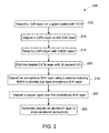
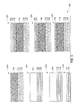
- an exemplary, non-limiting method 200 of forming an n-p-p+ device 222 is provided.
- a CdS layer 114 is deposited on glass 110 that is coated with a transparent conductive oxide 112.
- the CdS layer 114 is coated using the CSS technique.
- a CdTe layer 310 having a thickness of about 3 microns to about 5 microns is deposited on the top of the CdS layer 114 using a CSS technique.
- the CdTe layer 310 is exposed to a CdC1 2 treatment to provide a CdTe layer 312 with higher carrier density.
- a fourth step 216 the CdC1 2 treated CdTe layer 312 is etched using 30 percent concentrate hydrochloric acid to provide a stoichiometric CdTe layer 116.
- a p+ layer a-Si:H 118 is deposited over the CdTe layer 116 using a PECVD technique where the plasma containing the a-Si:H is intermixed with B 2 H 6 to control the boron and carbon concentration in the p+-type layer 118.
- a metal layer is deposited on the surface of the p+-type layer 118 to form the back contact layer.
- the metal layer could be topped with 100 nanometers of an aluminum layer 314 to improve lateral conductivity.
- a method 300 to form an n-i-p+ device 222 is provided.
- the method is similar to that discussed above for forming the n-p-p+ device except in that the time of the etch or the amount of the CdTe layer 312 etched is such that less than 2 micron of CdTe is left behind to form the absorber layer 116.
- the thickness of the CdTe layer left behind is such that the grain-boundaries are not opened, i.e., no pinholes are formed in the CdTe layer.
- the grain boundaries will etch faster than the grains, resulting in pinholes in the CdTe layer, for example, formation of pinholes at grain boundaries near the surface of the CdTe layer, if proper thickness control is not maintained.
- a method to form an n-i-p+ device 222 is provided.
- the method is similar to that discussed above for forming the n-p-p+ device except in that the initial thickness of the CdTe layer 310 as deposited is less than 1-2 micrometers and the time of the CdC1 2 treatment is made significantly shorter as the required carrier density is achieved and the carrier density does not need to be optimized. Also the etching of the resultant CdTe layer 312 to form the CdTe layer 116 is done such that the etch does not attack the grain boundaries.
- HCI chemical vapor deposition
- the photovoltaic device is a photovoltaic cell or a photovoltaic module.
- the photovoltaic device 100 produced as discussed typically requires further features to be used for practical electricity generation. That is, a terminal may be formed through which the generated electric power is led and a means for consuming or storing it. Alternatively, since a single power-generating cell usually has a low generated voltage, it may be desirable to form terminals for making voltage higher by connecting the photovoltaic devices in series. Accordingly, an insulating layer is provided to ensure insulation between the substrate and the photovoltaic device 100.
- a terminal made of, for example, a thick foil of a metal is connected to the back contact layer 120 of the photovoltaic device 100 using a conductive adhesive or other suitable connection means so that it can be used as a power-withdrawing terminal or a terminal for connecting in series another adjoining photovoltaic device constituted similarly.
- a solar panel i.e., a photovoltaic module comprising a plurality of photovoltaic devices as described above may be assembled in series to form a photovoltaic module.
Landscapes
- Photovoltaic Devices (AREA)
Applications Claiming Priority (1)
| Application Number | Priority Date | Filing Date | Title |
|---|---|---|---|
| US12/612,271 US20110100447A1 (en) | 2009-11-04 | 2009-11-04 | Layer for thin film photovoltaics and a solar cell made therefrom |
Publications (1)
| Publication Number | Publication Date |
|---|---|
| EP2320480A2 true EP2320480A2 (fr) | 2011-05-11 |
Family
ID=43501132
Family Applications (1)
| Application Number | Title | Priority Date | Filing Date |
|---|---|---|---|
| EP10189301A Withdrawn EP2320480A2 (fr) | 2009-11-04 | 2010-10-28 | Couche pour photovoltaïques à couche mince et cellule solaire fabriquée à partir de la couche |
Country Status (4)
| Country | Link |
|---|---|
| US (1) | US20110100447A1 (fr) |
| EP (1) | EP2320480A2 (fr) |
| CN (1) | CN102074594A (fr) |
| AU (1) | AU2010241208A1 (fr) |
Cited By (1)
| Publication number | Priority date | Publication date | Assignee | Title |
|---|---|---|---|---|
| EP2969273A4 (fr) * | 2013-03-15 | 2016-10-12 | First Solar Inc | Procédé de fabrication d'un dispositif photovoltaïque |
Families Citing this family (12)
| Publication number | Priority date | Publication date | Assignee | Title |
|---|---|---|---|---|
| US8524524B2 (en) * | 2010-04-22 | 2013-09-03 | General Electric Company | Methods for forming back contact electrodes for cadmium telluride photovoltaic cells |
| US9461186B2 (en) | 2010-07-15 | 2016-10-04 | First Solar, Inc. | Back contact for a photovoltaic module |
| WO2013043809A2 (fr) * | 2011-09-21 | 2013-03-28 | Arizona Board Of Regents, A Body Corporate Of The State Of Arizona | Cellules solaires si à hétérostructure utilisant des semi-conducteurs à large bande interdite |
| JP2013235890A (ja) * | 2012-05-07 | 2013-11-21 | Denso Corp | 半導体装置 |
| US9871154B2 (en) | 2013-06-21 | 2018-01-16 | First Solar, Inc. | Photovoltaic devices |
| CN103872178B (zh) * | 2014-02-28 | 2016-07-06 | 江苏武进汉能光伏有限公司 | 一种薄膜太阳能电池及组件、以及二者的制备方法 |
| CN104362194A (zh) * | 2014-12-08 | 2015-02-18 | 中国科学技术大学 | 背接触层结构及包含其的CdTe太阳能电池 |
| CN108321229A (zh) * | 2018-03-26 | 2018-07-24 | 赵博阳 | 一种太阳能电池 |
| CN112889216A (zh) * | 2018-10-17 | 2021-06-01 | 瑞士应用科技大学(Supsi) | 特别用于窗等的建筑物集成光伏设备、用于所述设备的方法和板条 |
| IL309370B2 (en) | 2021-06-16 | 2025-07-01 | Conti Spe Llc | Mechanically stacked solar transmissive cells or modules |
| CN118800820B (zh) * | 2024-09-13 | 2024-12-13 | 龙焱能源科技(杭州)股份有限公司 | 一种薄膜光伏组件及其制备方法 |
| US12414402B1 (en) | 2025-01-03 | 2025-09-09 | Conti Innovation Center, Llc | Optimizing cadmium (CD) alloy solar cells with sputtered copper-dopped zinc telluride (ZNTE:CU) back contacts in the presence of hydrogen |
Family Cites Families (10)
| Publication number | Priority date | Publication date | Assignee | Title |
|---|---|---|---|---|
| JPS5591885A (en) * | 1978-12-28 | 1980-07-11 | Canon Inc | Amorphous silicon hydride photoconductive layer |
| CA2024662A1 (fr) * | 1989-09-08 | 1991-03-09 | Robert Oswald | Module photovoltaique monolithique a elements montes en serie et en parallele |
| US5261968A (en) * | 1992-01-13 | 1993-11-16 | Photon Energy, Inc. | Photovoltaic cell and method |
| US5916375A (en) * | 1995-12-07 | 1999-06-29 | Japan Energy Corporation | Method of producing photoelectric conversion device |
| US5909632A (en) * | 1997-09-25 | 1999-06-01 | Midwest Research Institute | Use of separate ZnTe interface layers to form OHMIC contacts to p-CdTe films |
| JP3364180B2 (ja) * | 1999-01-18 | 2003-01-08 | 三菱重工業株式会社 | 非晶質シリコン太陽電池 |
| US7259321B2 (en) * | 2002-01-07 | 2007-08-21 | Bp Corporation North America Inc. | Method of manufacturing thin film photovoltaic modules |
| US7202143B1 (en) * | 2003-10-23 | 2007-04-10 | The Board Of Trustees Of The University Of Arkansas | Low temperature production of large-grain polycrystalline semiconductors |
| US20090020149A1 (en) * | 2007-07-16 | 2009-01-22 | Woods Lawrence M | Hybrid Multi-Junction Photovoltaic Cells And Associated Methods |
| CN102257633A (zh) * | 2008-12-18 | 2011-11-23 | 第一太阳能有限公司 | 包括背面金属接触的光伏器件 |
-
2009
- 2009-11-04 US US12/612,271 patent/US20110100447A1/en not_active Abandoned
-
2010
- 2010-10-28 EP EP10189301A patent/EP2320480A2/fr not_active Withdrawn
- 2010-11-03 AU AU2010241208A patent/AU2010241208A1/en not_active Abandoned
- 2010-11-04 CN CN2010105452187A patent/CN102074594A/zh active Pending
Non-Patent Citations (1)
| Title |
|---|
| None |
Cited By (1)
| Publication number | Priority date | Publication date | Assignee | Title |
|---|---|---|---|---|
| EP2969273A4 (fr) * | 2013-03-15 | 2016-10-12 | First Solar Inc | Procédé de fabrication d'un dispositif photovoltaïque |
Also Published As
| Publication number | Publication date |
|---|---|
| US20110100447A1 (en) | 2011-05-05 |
| AU2010241208A1 (en) | 2011-05-19 |
| CN102074594A (zh) | 2011-05-25 |
Similar Documents
| Publication | Publication Date | Title |
|---|---|---|
| EP2320480A2 (fr) | Couche pour photovoltaïques à couche mince et cellule solaire fabriquée à partir de la couche | |
| US20110143489A1 (en) | Process for making thin film solar cell | |
| AU2011203136B2 (en) | Photovoltaic cell and methods for forming a back contact for a photovoltaic cell | |
| US20130104985A1 (en) | Photovoltaic device with mangenese and tellurium interlayer | |
| EP2237323A2 (fr) | Couche pour photovoltaïques à couche mince et cellule solaire fabriquée à partir de la couche | |
| WO2010059950A1 (fr) | Procédé et structure pour cellule photovoltaïque à couche mince utilisant une jonction de matériaux similaires | |
| EP2482329A2 (fr) | Dispositif photovoltaïque | |
| WO2010039727A1 (fr) | Procédé et structure pour cellule photovoltaïque tandem à film mince | |
| AU2012203186A1 (en) | Photovoltaic devices and method of making | |
| CN103855232B (zh) | 光伏器件及其制造方法 | |
| US8785232B2 (en) | Photovoltaic device | |
| EP2973742A2 (fr) | Dispositifs photovoltaïques et procédé de réalisation | |
| WO2013106439A1 (fr) | Couches tampon haute efficacité pour dispositifs photovoltaïques à base de silicium | |
| US20090301562A1 (en) | High efficiency photovoltaic cell and manufacturing method | |
| WO2014140875A2 (fr) | Procédé de fabrication de dispositifs photovoltaïques | |
| EP2962332A1 (fr) | Dispositifs photovoltaïques et procédés de fabrication | |
| US20140000673A1 (en) | Photovoltaic device and method of making | |
| Kaliyannan et al. | Thin‐film solar cells | |
| AU2012203590A1 (en) | Methods of making photovoltaic devices and photovoltaic devices | |
| US9087943B2 (en) | High efficiency photovoltaic cell and manufacturing method free of metal disulfide barrier material | |
| US20140060608A1 (en) | Photovoltaic device and method of making | |
| KR101684800B1 (ko) | 플라즈마처리를 이용한 CdTe 박막형성방법 및 이에 의해 제조된 CdTe 태양전지 |
Legal Events
| Date | Code | Title | Description |
|---|---|---|---|
| PUAI | Public reference made under article 153(3) epc to a published international application that has entered the european phase |
Free format text: ORIGINAL CODE: 0009012 |
|
| AK | Designated contracting states |
Kind code of ref document: A2 Designated state(s): AL AT BE BG CH CY CZ DE DK EE ES FI FR GB GR HR HU IE IS IT LI LT LU LV MC MK MT NL NO PL PT RO RS SE SI SK SM TR |
|
| AX | Request for extension of the european patent |
Extension state: BA ME |
|
| STAA | Information on the status of an ep patent application or granted ep patent |
Free format text: STATUS: THE APPLICATION IS DEEMED TO BE WITHDRAWN |
|
| 18D | Application deemed to be withdrawn |
Effective date: 20130503 |