EP2320536A1 - Dispositif de contrôle de module de stockage d'énergie électrique - Google Patents
Dispositif de contrôle de module de stockage d'énergie électrique Download PDFInfo
- Publication number
- EP2320536A1 EP2320536A1 EP10186820A EP10186820A EP2320536A1 EP 2320536 A1 EP2320536 A1 EP 2320536A1 EP 10186820 A EP10186820 A EP 10186820A EP 10186820 A EP10186820 A EP 10186820A EP 2320536 A1 EP2320536 A1 EP 2320536A1
- Authority
- EP
- European Patent Office
- Prior art keywords
- voltage
- energy storage
- electric energy
- storage module
- capacitor
- Prior art date
- Legal status (The legal status is an assumption and is not a legal conclusion. Google has not performed a legal analysis and makes no representation as to the accuracy of the status listed.)
- Withdrawn
Links
Images

Classifications
-
- H—ELECTRICITY
- H02—GENERATION; CONVERSION OR DISTRIBUTION OF ELECTRIC POWER
- H02J—ELECTRIC POWER NETWORKS; CIRCUIT ARRANGEMENTS OR SYSTEMS FOR SUPPLYING OR DISTRIBUTING ELECTRIC POWER; SYSTEMS FOR STORING ELECTRIC ENERGY
- H02J7/00—Circuit arrangements for charging or discharging batteries or for supplying loads from batteries
- H02J7/50—Circuit arrangements for charging or discharging batteries or for supplying loads from batteries acting upon multiple batteries simultaneously or sequentially
- H02J7/52—Circuit arrangements for charging or discharging batteries or for supplying loads from batteries acting upon multiple batteries simultaneously or sequentially for charge balancing, e.g. equalisation of charge between batteries
- H02J7/54—Passive balancing, e.g. using resistors or parallel MOSFETs
Definitions
- the present invention relates to an electric energy storage module control device for controlling a voltage of an electric energy storage module including a plurality of capacitors connected in series.
- a voltage limiting circuit for, if the capacitor has been charged to a voltage exceeding its upper limit voltage, discharging the capacitor so as to reduce the voltage thereof to the upper limit voltage.
- a voltage limiting circuit includes, for example, a Zener diode or a shunt regulator, and is connected in parallel to each capacitor (see, for example, FIGS. 5(b) and 5(c) of Japanese Patent No. 3244592 , and Japanese Patent Application Laid-open Nos. Hei 06-261452 and 2005-101434 ). According to this method, each capacitor is prevented from being over-charged, to thereby delay the progress of degradation of the capacitor.
- FIG. 5(a) of Japanese Patent No. 3244592 illustrates a voltage control circuit which is formed of resistors having the same resistance and connected in parallel to each capacitor. Owing to a current flowing through those resistors, a voltage of the whole electric energy storage module is equally divided among the capacitors.
- the capacitor voltages may be controlled to be equalized all the time, regardless of the magnitude of the voltage of the whole electric energy storage module.
- a current flows continuously via the resistors all the time, leading to wasted power consumption, which causes a problem that the capacitor may suffer large voltage drop while the electric energy storage module is not in use.
- the resistance of the resistor is increased to suppress such power consumption, the ability to equalize the capacitor voltages lowers.
- the present invention has been made in view of the above-mentioned circumstances, and one of the objects thereof is to provide an electric energy storage module control device having low power consumption, which is capable of equalizing capacitor voltages even while the capacitor voltages are equal to or lower than upper limit voltages thereof.
- the present invention provides an electric energy storage module control device for controlling an electric energy storage module including a plurality of capacitors connected in series, the electric energy storage module control device including a voltage control circuit connected in parallel to each of the plurality of capacitors, in which: the voltage control circuit includes: a constant voltage control part for controlling and preventing a voltage across the constant voltage control part from exceeding a predetermined voltage; and a resistor connected in series to the constant voltage control part; and the predetermined voltage is lower than an upper limit applied voltage of each of the plurality of capacitors.
- the constant voltage control part may include a shunt regulator.
- the shunt regulator may include a cathode terminal, an anode terminal, and a reference voltage terminal, and the reference voltage terminal may be directly connected to the cathode terminal.
- the predetermined voltage may be between 50% or more and 85% or less with respect to the upper limit applied voltage of each of the plurality of capacitors.
- the resistor may have a resistance of between 2 ⁇ or larger and 50 ⁇ or smaller. Further, the resistor may have a resistance of between 5 ⁇ or larger and 10 ⁇ or smaller.
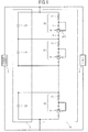
- FIG. 1 is a diagram illustrating a circuit configuration of an electric energy storage module control device 1a according to a first embodiment of the present invention.
- An electric energy storage module 2 to be controlled by the electric energy storage module control device 1a according to this embodiment includes a plurality of capacitors 20 connected in series to one another. It should be noted that in this embodiment, N capacitors 20 are connected in series.
- Each of the capacitors 20 is an electric energy storage device, such as an electric double layer capacitor, which is capable of storing power when supplied with a current.
- the N capacitors 20 are of the same type and the same capacitance.
- To charge the electric energy storage module 2 a voltage is applied across both end terminals thereof from an external power source 3. Power is storaged in the electric energy storage module 2 and utilized for driving a load 4.
- the electric energy storage module control device 1a includes the same number of (N) voltage control circuits 10 as the capacitors 20 forming the electric energy storage module 2.
- the voltage control circuits 10 are connected in parallel to the capacitors 20 on a one-on-one basis.
- Each of the voltage control circuits 10 includes a resistor 12 and a constant voltage control part 14 connected in series to the resistor 12.
- N resistors 12 have the same resistance (hereinafter, referred to as resistance R).
- the constant voltage control part 14 controls a voltage across the constant voltage control part 14 so as not to exceed a predetermined voltage.
- the predetermined voltage is referred to as an operating voltage V s of the constant voltage control part 14.
- capacitor voltage V c a voltage of the capacitor 20
- V c a voltage of the constant voltage control part 14 included in the voltage control circuit 10 connected in parallel to the capacitor 20
- a voltage (V c -V s ) corresponding to a difference between the capacitor voltage V c and the operating voltage V s of the constant voltage control part 14 is applied across the resistor 12 connected in series to the constant voltage control part 14.
- N constant voltage control parts 14 have the same operating voltage V s .
- the constant voltage control part 14 does not allow a current to flow unless the voltage applied thereacross becomes the operating voltage V s or higher. Accordingly, while the capacitor voltage V c is lower than the operating voltage V s , no current flows through the voltage control circuit 10 connected in parallel to the capacitor 20.
- the constant voltage control part 14 includes a shunt regulator. As illustrated in FIG. 1 , the shunt regulator includes both end terminals (cathode terminal K and anode terminal A) and a reference voltage terminal REF (reference terminal) , as connection terminals to the outside.
- the shunt regulator has a built-in reference voltage (hereinafter, referred to as internal reference voltage V ref ), and operates so that the reference voltage terminal REF has a voltage equal to the internal reference voltage V ref .
- the cathode terminal K of the shunt regulator is connected to one end of the resistor 12, and the anode terminal A thereof is connected to one end of the capacitor 20. Another end of the resistor 12 is connected to another end of the capacitor 20. Further, in this embodiment, the reference voltage terminal REF of the shunt regulator is directly connected to the cathode terminal K. With this configuration, feedback control is made on the current flowing through the shunt regulator so that the cathode terminal K has a voltage equal to the internal reference voltage V ref of the shunt regulator. In other words, in this embodiment, the operating vol tage V s of the constant voltage control part 14 is equal to the internal reference voltage V ref of the shunt regulator.
- the electric energy storage module 2 is charged until the voltage across the electric energy storage module 2 reaches a voltage V m , which is N ⁇ V s or higher. Then, when the capacitor voltage V c of the capacitor 20 becomes the operating voltage V s or higher, a current starts to flow through the shunt regulator included in the corresponding voltage control circuit 10. At this time, the voltage across the constant voltage control part 14 is maintained at the operating voltage V s , which is constant regardless of fluctuations in the capacitor voltage V c .
- a voltage (V m -N ⁇ V s ) corresponding to a difference between the voltage V m of the whole electric energy storage module 2 and the total value N ⁇ V s of the voltages generated across the N constant voltage control parts 14 is divided by the N resistors 12.
- the resistors 12 have the same resistance R, and hence the voltage (V m -N ⁇ V s ) is equally divided by the resistors 12.
- the resistors 12 have the same voltage V r generated thereacross.
- the voltage control circuits 10 have the same voltage generated thereacross. This way, the capacitor voltages V c of the capacitors 20 are equalized.
- the capacitor voltage V c in this case is expressed as follows.
- the capacitor voltage V c is divided by the resistor 12 and the constant voltage control part 14 within the voltage control circuit 10, and hence the voltage V r generated by the resistor 12 is the voltage (V c -V s ), which is lower than the capacitor voltage V c . Therefore, according to the electric energy storage module control device 1a of this embodiment, a small current flows through the resistor 12 compared with a case where the same voltage as the capacitor voltage V c is applied across the resistor 12.
- the current stops flowing through the voltage control circuit 10. Accordingly, even if a current flows through the voltage control circuit 10 to discharge the capacitor 20 when the electric energy storage module 2 is not in use, the discharge via the voltage control circuit 10 may stop at a time when the capacitor voltage V c reduces to the operating voltage V s . Therefore, further power consumption of the voltage control circuit 10 is prevented, to thereby suppress voltage drop of the capacitor 20 due to the voltage control circuit 10.
- the operating Voltage V s of each constant voltage control part 14 is desired to have a value of 50% or more and 85% or less with respect to an upper limit voltage V max of the capacitor 20.
- the upper limit voltage V max of the capacitor 20 is a voltage of the capacitor 20 which is determined when the electric energy storage module 2 has been fully charged under a normal usage environment, that is, a maximum allowable applied voltage of the capacitor 20.
- the upper limit voltage V max may be set to a rated voltage value specified by a manufacturer of the capacitor 20.
- the rated voltage may be defined by a value which is determined according to JIS D 1401:2009 at an environmental temperature of 60°C to 80°C.
- FIG. 2 is a graph illustrating an example of a temporal change in the capacitor voltage V c , which is caused by such charge/discharge.
- the operating voltage V s is set too low with respect to the upper limit voltage V max , the voltage V r applied across the resistor 12 becomes large when the capacitor 20 is almost fully charged, resulting in an increase in consumption current flowing through the resistor 12. For that reason, the operating voltage V s is desired to be 50% or more of the upper limit voltage V max of the capacitor 20.
- the operating voltage V s of the constant voltage control part 14 is set too high, output energy of the capacitor 20 reduces in the case where the capacitor 20 is discharged from the fully-charged state (state in which the capacitor voltage V c is equal to the upper limit voltage V max ) until the capacitor voltage V c becomes equal to the operating voltage V s . For that reason, the operating voltage V s is desired to be 85% or less of the upper limit voltage V max of the capacitor 20.
- each capacitor 20 may output energy within a range from about 75% to about 28% with respect to energy of the capacitor 20 storaged by the time of full charge. It should be noted that in a case of a normal battery, considering the influence on the life etc., charge/discharge is performed with energy within a range of about 30% with respect to the storaged energy at the time of full charge.
- each resistor 12 is preferably 2 ⁇ or larger and 50 ⁇ or smaller, more preferably 2 ⁇ or larger and 20 ⁇ or smaller, still more preferably 5 ⁇ or larger and 10 ⁇ or smaller.
- the resistance R As the resistance R becomes smaller, the current flowing through the resistor 12 becomes larger, resulting in wasted current consumption. Therefore, from the viewpoint of suppressing the current consumption due to the resistor 12, the resistance R needs to be large to some extent. Specifically, the voltage V r generated across the resistor 12 when the electric energy storage module 2 is fully charged is equal to a difference (V max -V s ) between the upper limit voltage V max of the capacitor 20 and the operating voltage V s of the constant voltage control part 14.
- the resistance R is preferably 2 ⁇ or larger, more preferably 5 ⁇ or larger. It should be noted that in a case where priority is placed on suppressing the current consumption, the resistance R may be 10 ⁇ or larger.
- Capacitors 20 have variations in amount of leakage current due to variations in electrostatic capacitance and temperature during their use.
- the variations in leakage current are mainly responsible for the variations in capacitor voltages V c among the capacitors 20.
- the variations in leakage current are compensated with the current flowing through the resistors 12.
- a maximum leakage current difference among the capacitors 20 is represented by ⁇ I L
- the electric energy storage module control device 1a operates so that a voltage difference ⁇ V c in capacitor voltage V c generated among the capacitors 20 converges within a value expressed as follows.
- ⁇ ⁇ V c ⁇ ⁇ I L ⁇ R
- the voltage difference ⁇ V c is proportional to the resistance R.
- the capacitor voltages V c may converge to the same value with more accuracy.
- the equalizing ability of the electric energy storage module control device 1a increases more.
- the resistance R is preferably 50 ⁇ or smaller, more preferably 20 ⁇ or smaller. It should be noted that in a case where priority is placed on equalizing the capacitor voltages V c , the resistance R may be 10 ⁇ or smaller.
- the resistance R is set to 2 ⁇ or larger and 50 ⁇ or smaller, more preferably 2 ⁇ or larger and 20 ⁇ or smaller. In those ranges, the resistance R may be set to 2 ⁇ or larger and 10 ⁇ or smaller for use with priority given to the equalization of the capacitor voltages V c , while the resistance R may be set to 10 ⁇ or larger and 20 ⁇ or smaller for use with priority given to the suppression in current consumption. Further, in a case where the requirements of both the increase in equalizing ability and the suppression in current consumption need to be satisfied in a balanced manner, the resistance R is preferably set to 5 ⁇ or larger and 10 ⁇ or smaller.
- FIG. 3 is a graph illustrating a relationship between the resistance R and the current consumption, and a relationship between the resistance R and the voltage difference ⁇ V c among the capacitors 20 at the time of convergence.
- the solid line indicates the relationship between the resistance R and the current consumption
- the broken line indicates the relationship between the resistance R and the voltage difference ⁇ V c .
- the horizontal axis represents the resistance R ( ⁇ )
- the left-hand vertical axis represents the voltage difference ⁇ V c (mV) while the right-hand vertical axis represents the current consumption (mA).
- the leakage current difference ⁇ I L among the capacitors 20 is assumed to be 5 mA.
- the current consumption becomes larger inversely.
- the voltage difference ⁇ V c increases. Further, centering around the position of an intersection between the solid line and the broken line, in the range of the resistance R between 5 ⁇ or larger and 10 ⁇ or smaller, the voltage difference ⁇ V c takes 50 mV or smaller and the current consumption takes 100 mA or smaller, leading to the understanding that the requirements of both the increase in equalizing ability and the suppression in current consumption are satisfied.
- the capacitor voltages V c of the capacitors 20 may be controlled to be substantially equal to one another. Further, compared with the case where only the resistor 12 is connected in parallel to each capacitor 20, the current consumption of the voltage control circuit 10 may be suppressed to be low. Also, as long as the capacitor voltage V c is equal to or lower than the operating voltage V s , the current consumption of the voltage control circuit 10 may be reduced to 0.
- the resistor 12 limits the current flowing through the voltage control circuit 10, and hence the breakage of the circuit elements due to overcharge of the capacitor 20 may be prevented.
- an electric energy storage module control device 1b according to a second embodiment of the present invention will be described. It should be noted that the description of the electric energy storage module control device 1b according to this embodiment is mainly directed to a difference from the first embodiment, omitting the same configuration and function as the electric energy storage module control device 1a according to the first embodiment.
- the same components as the first embodiment are denoted by the same reference symbols.
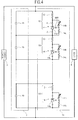
- FIG. 4 is a circuit diagram illustrating a circuit configuration of the electric energy storage module control device 1b according to this embodiment.
- the electric energy storage module 2 including the capacitors 20 connected in series to one another.
- the voltage control circuits 10 are connected in parallel to the capacitors 20, respectively, and each include the resistor 12 and the constant voltage control part 14 connected in series to each other.
- the constant voltage control part 14 includes, in addition to a shunt regulator 14a, two resistors 14b and 14c connected in series to each other.
- One terminal of the resistor 14b is connected to a cathode terminal Kof the shunt regulator 14a, and another terminal thereof is connected to one terminal of the resistor 14c and a reference voltage terminal REF of the shunt regulator 14a.
- Another terminal of the resistor 14c is connected to an anode terminal A of the shunt regulator 14a.
- the operating voltage V s of the whole constant voltage control part 14 takes an approximate value expressed by the following expression.
- V s 1 + R ⁇ 1 / R ⁇ 2 ⁇ V ref
- R1 represents a resistance of the resistor 14b
- R2 represents a resistance of the resistor 14c
- V ref represents an internal reference voltage of the shunt regulator 14a.
- the constant voltage control part 14 operates with the operating voltage V s , which is determined in accordance with the resistances R1 and R2. In other words, the voltage across the constant voltage control part 14 is controlled so as not to exceed the operating voltage V s .
- the constant voltage control part 14 is allowed to operate with the operating voltage V s which is different from the internal reference voltage V ref built in the shunt regulator 14a.
- At least one of the resistors 14b and 14c employs a variable resistor to adjust its resistance, to thereby appropriately adjust the operating voltage V s of the constant voltage control part 14 with no modification to the circuit configuration.
- FIG. 4 illustrates the case where the resistor 14b is a variable resistor.
- the embodiments of the present invention are not limited to what has been described above.
- the constant voltage control part 14 may have a different circuit configuration from those of the first and second embodiments.
- the capacitor 20 included in the electric energy storage module 2 and connected in parallel to the corresponding voltage control circuit 10 may be a capacitor module in which a plurality of capacitor cells are connected to each other.
- the capacitors 20 in the circuit configuration illustrated in FIG. 1 , as the capacitors 20, five electric double layer capacitors, manufactured by Nisshinbo Holdings Inc., having a capacitance of 250 F and a rated voltage of 3.0 V were connected in series to form the electric energy storage module 2. Further, in the circuit configuration illustrated in FIG. 1 , as the capacitors 20, five electric double layer capacitors, manufactured by Nisshinbo Holdings Inc., having a capacitance of 250 F and a rated voltage of 3.0 V were connected in series to form the electric energy storage module 2. Further, in the circuit configuration illustrated in FIG.
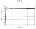
- FIG. 5 illustrates temporal changes in voltages of the capacitors 20 obtained when the electric energy storage module control device 1a was used to charge the electric energy storage module 2, starting from the state where the five capacitors 20 are completely discharged. As illustrated in FIG. 5 , it was found that, immediately after the start of charge of the capacitors 20, there are variations in capacitor voltages of the capacitors 20, but as time elapses, the voltage of each capacitor 20 converges to about 3 V, with the result that the voltages of the capacitors 20 are equalized.
Landscapes
- Engineering & Computer Science (AREA)
- Power Engineering (AREA)
- Charge And Discharge Circuits For Batteries Or The Like (AREA)
- Secondary Cells (AREA)
Applications Claiming Priority (1)
| Application Number | Priority Date | Filing Date | Title |
|---|---|---|---|
| JP2009240746A JP2011087448A (ja) | 2009-10-19 | 2009-10-19 | 蓄電モジュール制御装置 |
Publications (1)
| Publication Number | Publication Date |
|---|---|
| EP2320536A1 true EP2320536A1 (fr) | 2011-05-11 |
Family
ID=43481003
Family Applications (1)
| Application Number | Title | Priority Date | Filing Date |
|---|---|---|---|
| EP10186820A Withdrawn EP2320536A1 (fr) | 2009-10-19 | 2010-10-07 | Dispositif de contrôle de module de stockage d'énergie électrique |
Country Status (4)
| Country | Link |
|---|---|
| US (1) | US20110089909A1 (fr) |
| EP (1) | EP2320536A1 (fr) |
| JP (1) | JP2011087448A (fr) |
| CN (1) | CN102074977A (fr) |
Cited By (1)
| Publication number | Priority date | Publication date | Assignee | Title |
|---|---|---|---|---|
| EP2463998A4 (fr) * | 2009-08-07 | 2017-12-27 | Daikin Industries, Ltd. | Circuit de lissage de tension |
Families Citing this family (7)
| Publication number | Priority date | Publication date | Assignee | Title |
|---|---|---|---|---|
| DE102011079360A1 (de) * | 2011-07-19 | 2013-01-24 | Sb Limotive Company Ltd. | Vorrichtung und Verfahren zur Messung einer maximalen Zellspannung |
| US9281696B2 (en) * | 2013-02-27 | 2016-03-08 | Fu-Sheng Tsai | Current steering circuit and current steering method for controlling branch current flowing through branch |
| CN104184197B (zh) * | 2014-09-12 | 2017-04-19 | 上海海事大学 | 超级电容电压均衡电路及其均衡电容参数识别方法 |
| CN106999807B (zh) * | 2014-12-18 | 2019-12-20 | 康明斯过滤Ip公司 | 过滤装置的自动排放塞 |
| HK1243828A1 (zh) * | 2015-03-04 | 2018-07-20 | Maxwell Technologies, Inc. | 用於改进电池平衡以及电池故障检测的系统和方法 |
| TWI604681B (zh) * | 2016-10-11 | 2017-11-01 | 精威機電有限公司 | 具有充放電保護之電池成組裝置 |
| JP7738270B2 (ja) * | 2020-12-28 | 2025-09-12 | パナソニックIpマネジメント株式会社 | 蓄電デバイス制御回路と、それを用いたバックアップ電源システム |
Citations (7)
| Publication number | Priority date | Publication date | Assignee | Title |
|---|---|---|---|---|
| JPH06261452A (ja) | 1993-03-04 | 1994-09-16 | Jeol Ltd | 蓄電電源装置 |
| US5982144A (en) * | 1997-07-14 | 1999-11-09 | Johnson Research & Development Company, Inc. | Rechargeable battery power supply overcharge protection circuit |
| US6316917B1 (en) * | 1999-03-09 | 2001-11-13 | Asahi Glass Company, Limited | Apparatus having plural electric double layer capacitors and method for adjusting voltages of the capacitors |
| JP3244592B2 (ja) | 1994-05-25 | 2002-01-07 | 株式会社岡村研究所 | 電池の充電制御方法 |
| US6424156B1 (en) * | 1992-04-03 | 2002-07-23 | Jeol Ltd. | Storage capacitor power supply |
| US20030151389A1 (en) * | 2002-02-08 | 2003-08-14 | John Cummings | Electrical power source apparatuses, circuits, electrochemical device charging methods, and methods of charging a plurality of electrochemical devices |
| JP2005101434A (ja) | 2003-09-26 | 2005-04-14 | Meidensha Corp | 分担電圧均等化回路を有するキャパシタ装置 |
-
2009
- 2009-10-19 JP JP2009240746A patent/JP2011087448A/ja active Pending
-
2010
- 2010-10-01 US US12/896,312 patent/US20110089909A1/en not_active Abandoned
- 2010-10-07 EP EP10186820A patent/EP2320536A1/fr not_active Withdrawn
- 2010-10-19 CN CN2010105172025A patent/CN102074977A/zh active Pending
Patent Citations (7)
| Publication number | Priority date | Publication date | Assignee | Title |
|---|---|---|---|---|
| US6424156B1 (en) * | 1992-04-03 | 2002-07-23 | Jeol Ltd. | Storage capacitor power supply |
| JPH06261452A (ja) | 1993-03-04 | 1994-09-16 | Jeol Ltd | 蓄電電源装置 |
| JP3244592B2 (ja) | 1994-05-25 | 2002-01-07 | 株式会社岡村研究所 | 電池の充電制御方法 |
| US5982144A (en) * | 1997-07-14 | 1999-11-09 | Johnson Research & Development Company, Inc. | Rechargeable battery power supply overcharge protection circuit |
| US6316917B1 (en) * | 1999-03-09 | 2001-11-13 | Asahi Glass Company, Limited | Apparatus having plural electric double layer capacitors and method for adjusting voltages of the capacitors |
| US20030151389A1 (en) * | 2002-02-08 | 2003-08-14 | John Cummings | Electrical power source apparatuses, circuits, electrochemical device charging methods, and methods of charging a plurality of electrochemical devices |
| JP2005101434A (ja) | 2003-09-26 | 2005-04-14 | Meidensha Corp | 分担電圧均等化回路を有するキャパシタ装置 |
Non-Patent Citations (1)
| Title |
|---|
| FAIRCHILD SEMICONDUCTORS: "TL431/TL431A Programmable shunt regulator", 1 January 2003 (2003-01-01), pages 1 - 10, XP002619144, Retrieved from the Internet <URL:http://www.fairchildsemi.com/ds/TL/TL431A.pdf> [retrieved on 20110204] * |
Cited By (1)
| Publication number | Priority date | Publication date | Assignee | Title |
|---|---|---|---|---|
| EP2463998A4 (fr) * | 2009-08-07 | 2017-12-27 | Daikin Industries, Ltd. | Circuit de lissage de tension |
Also Published As
| Publication number | Publication date |
|---|---|
| JP2011087448A (ja) | 2011-04-28 |
| CN102074977A (zh) | 2011-05-25 |
| US20110089909A1 (en) | 2011-04-21 |
Similar Documents
| Publication | Publication Date | Title |
|---|---|---|
| US10714947B2 (en) | Systems and methods for controlling battery current | |
| US7522435B2 (en) | Power supply converter/s with controller/s responsive to voltage, current, and power | |
| US20110089909A1 (en) | Electric energy storage module control device | |
| US7400114B2 (en) | Voltage equalizer for battery elements | |
| JP4663811B2 (ja) | バッテリー装置の回路動作電流バランシング装置及び方法 | |
| JP2009044946A (ja) | 組電池の充電方法 | |
| TW201218576A (en) | Dc power supply device | |
| JP6196466B2 (ja) | 電源装置 | |
| JP2013520947A (ja) | バッテリセルコンバータ管理システム | |
| JP2010178591A (ja) | 充電回路、充電装置、電子機器及び充電方法 | |
| JPWO2013161512A1 (ja) | 充電制御装置および充電制御方法 | |
| JP6824295B2 (ja) | 電気機器 | |
| US9374077B2 (en) | Switch circuit, semiconductor device, and battery device | |
| WO2021215282A1 (fr) | Dispositif d'alimentation électrique sans interruption | |
| CN108336777A (zh) | 具有锂离子电容器的电源组件 | |
| WO2020115990A1 (fr) | Circuit de détermination de polarité de batterie, chargeur et dispositif électronique | |
| JP2009148110A (ja) | 充放電器とこれを用いた電源装置 | |
| JP2009296719A (ja) | 直流バックアップ電源システムおよびその充電方法 | |
| JP5295801B2 (ja) | 直流電源システムおよび放電方法 | |
| JP2016040999A (ja) | 蓄電池装置の充電状態均等化方法 | |
| JP4948907B2 (ja) | 電池システム | |
| JP2009171724A (ja) | 双方向コンバータ | |
| JP5359103B2 (ja) | 電力貯蔵装置の充放電制御方法 | |
| JP6380012B2 (ja) | 蓄電装置及び蓄電器の接続方法 | |
| JP2009153282A (ja) | バックアップ電源およびその制御方法 |
Legal Events
| Date | Code | Title | Description |
|---|---|---|---|
| PUAI | Public reference made under article 153(3) epc to a published international application that has entered the european phase |
Free format text: ORIGINAL CODE: 0009012 |
|
| AK | Designated contracting states |
Kind code of ref document: A1 Designated state(s): AL AT BE BG CH CY CZ DE DK EE ES FI FR GB GR HR HU IE IS IT LI LT LU LV MC MK MT NL NO PL PT RO RS SE SI SK SM TR |
|
| AX | Request for extension of the european patent |
Extension state: BA ME |
|
| 17P | Request for examination filed |
Effective date: 20111103 |
|
| 17Q | First examination report despatched |
Effective date: 20120216 |
|
| STAA | Information on the status of an ep patent application or granted ep patent |
Free format text: STATUS: THE APPLICATION IS DEEMED TO BE WITHDRAWN |
|
| 18D | Application deemed to be withdrawn |
Effective date: 20120828 |