EP2321894B1 - Generalisierte synchrone ac-dc-gleichrichtungsverfahren für einzelphasensysteme - Google Patents
Generalisierte synchrone ac-dc-gleichrichtungsverfahren für einzelphasensysteme Download PDFInfo
- Publication number
- EP2321894B1 EP2321894B1 EP09807881.9A EP09807881A EP2321894B1 EP 2321894 B1 EP2321894 B1 EP 2321894B1 EP 09807881 A EP09807881 A EP 09807881A EP 2321894 B1 EP2321894 B1 EP 2321894B1
- Authority
- EP
- European Patent Office
- Prior art keywords
- current
- voltage
- active switch
- rectifier
- diode
- Prior art date
- Legal status (The legal status is an assumption and is not a legal conclusion. Google has not performed a legal analysis and makes no representation as to the accuracy of the status listed.)
- Active
Links
Images













Classifications
-
- H—ELECTRICITY
- H02—GENERATION; CONVERSION OR DISTRIBUTION OF ELECTRIC POWER
- H02M—APPARATUS FOR CONVERSION BETWEEN AC AND AC, BETWEEN AC AND DC, OR BETWEEN DC AND DC, AND FOR USE WITH MAINS OR SIMILAR POWER SUPPLY SYSTEMS; CONVERSION OF DC OR AC INPUT POWER INTO SURGE OUTPUT POWER; CONTROL OR REGULATION THEREOF
- H02M7/00—Conversion of AC power input into DC power output; Conversion of DC power input into AC power output
- H02M7/02—Conversion of AC power input into DC power output without possibility of reversal
- H02M7/04—Conversion of AC power input into DC power output without possibility of reversal by static converters
- H02M7/12—Conversion of AC power input into DC power output without possibility of reversal by static converters using discharge tubes with control electrode or semiconductor devices with control electrode
- H02M7/21—Conversion of AC power input into DC power output without possibility of reversal by static converters using discharge tubes with control electrode or semiconductor devices with control electrode using devices of a triode or transistor type requiring continuous application of a control signal
- H02M7/217—Conversion of AC power input into DC power output without possibility of reversal by static converters using discharge tubes with control electrode or semiconductor devices with control electrode using devices of a triode or transistor type requiring continuous application of a control signal using semiconductor devices only
- H02M7/219—Conversion of AC power input into DC power output without possibility of reversal by static converters using discharge tubes with control electrode or semiconductor devices with control electrode using devices of a triode or transistor type requiring continuous application of a control signal using semiconductor devices only in a bridge configuration
-
- H—ELECTRICITY
- H03—ELECTRONIC CIRCUITRY
- H03K—PULSE TECHNIQUE
- H03K17/00—Electronic switching or gating, i.e. not by contact-making and –breaking
- H03K17/06—Modifications for ensuring a fully conducting state
-
- H—ELECTRICITY
- H03—ELECTRONIC CIRCUITRY
- H03K—PULSE TECHNIQUE
- H03K17/00—Electronic switching or gating, i.e. not by contact-making and –breaking
- H03K17/30—Modifications for providing a predetermined threshold before switching
- H03K17/302—Modifications for providing a predetermined threshold before switching in field-effect transistor switches
-
- H—ELECTRICITY
- H03—ELECTRONIC CIRCUITRY
- H03K—PULSE TECHNIQUE
- H03K17/00—Electronic switching or gating, i.e. not by contact-making and –breaking
- H03K17/51—Electronic switching or gating, i.e. not by contact-making and –breaking characterised by the components used
- H03K17/74—Electronic switching or gating, i.e. not by contact-making and –breaking characterised by the components used by the use, as active elements, of diodes
-
- H—ELECTRICITY
- H02—GENERATION; CONVERSION OR DISTRIBUTION OF ELECTRIC POWER
- H02M—APPARATUS FOR CONVERSION BETWEEN AC AND AC, BETWEEN AC AND DC, OR BETWEEN DC AND DC, AND FOR USE WITH MAINS OR SIMILAR POWER SUPPLY SYSTEMS; CONVERSION OF DC OR AC INPUT POWER INTO SURGE OUTPUT POWER; CONTROL OR REGULATION THEREOF
- H02M1/00—Details of apparatus for conversion
- H02M1/0083—Converters characterised by their input or output configuration
- H02M1/0085—Partially controlled bridges
-
- H—ELECTRICITY
- H02—GENERATION; CONVERSION OR DISTRIBUTION OF ELECTRIC POWER
- H02M—APPARATUS FOR CONVERSION BETWEEN AC AND AC, BETWEEN AC AND DC, OR BETWEEN DC AND DC, AND FOR USE WITH MAINS OR SIMILAR POWER SUPPLY SYSTEMS; CONVERSION OF DC OR AC INPUT POWER INTO SURGE OUTPUT POWER; CONTROL OR REGULATION THEREOF
- H02M1/00—Details of apparatus for conversion
- H02M1/08—Circuits specially adapted for the generation of control voltages for semiconductor devices incorporated in static converters
-
- H—ELECTRICITY
- H02—GENERATION; CONVERSION OR DISTRIBUTION OF ELECTRIC POWER
- H02M—APPARATUS FOR CONVERSION BETWEEN AC AND AC, BETWEEN AC AND DC, OR BETWEEN DC AND DC, AND FOR USE WITH MAINS OR SIMILAR POWER SUPPLY SYSTEMS; CONVERSION OF DC OR AC INPUT POWER INTO SURGE OUTPUT POWER; CONTROL OR REGULATION THEREOF
- H02M7/00—Conversion of AC power input into DC power output; Conversion of DC power input into AC power output
- H02M7/02—Conversion of AC power input into DC power output without possibility of reversal
- H02M7/04—Conversion of AC power input into DC power output without possibility of reversal by static converters
- H02M7/12—Conversion of AC power input into DC power output without possibility of reversal by static converters using discharge tubes with control electrode or semiconductor devices with control electrode
- H02M7/21—Conversion of AC power input into DC power output without possibility of reversal by static converters using discharge tubes with control electrode or semiconductor devices with control electrode using devices of a triode or transistor type requiring continuous application of a control signal
- H02M7/217—Conversion of AC power input into DC power output without possibility of reversal by static converters using discharge tubes with control electrode or semiconductor devices with control electrode using devices of a triode or transistor type requiring continuous application of a control signal using semiconductor devices only
- H02M7/219—Conversion of AC power input into DC power output without possibility of reversal by static converters using discharge tubes with control electrode or semiconductor devices with control electrode using devices of a triode or transistor type requiring continuous application of a control signal using semiconductor devices only in a bridge configuration
- H02M7/2195—Conversion of AC power input into DC power output without possibility of reversal by static converters using discharge tubes with control electrode or semiconductor devices with control electrode using devices of a triode or transistor type requiring continuous application of a control signal using semiconductor devices only in a bridge configuration the switches being synchronously commutated at the same frequency of the AC input voltage
-
- H—ELECTRICITY
- H03—ELECTRONIC CIRCUITRY
- H03K—PULSE TECHNIQUE
- H03K17/00—Electronic switching or gating, i.e. not by contact-making and –breaking
- H03K17/30—Modifications for providing a predetermined threshold before switching
- H03K2017/307—Modifications for providing a predetermined threshold before switching circuits simulating a diode, e.g. threshold zero
-
- Y—GENERAL TAGGING OF NEW TECHNOLOGICAL DEVELOPMENTS; GENERAL TAGGING OF CROSS-SECTIONAL TECHNOLOGIES SPANNING OVER SEVERAL SECTIONS OF THE IPC; TECHNICAL SUBJECTS COVERED BY FORMER USPC CROSS-REFERENCE ART COLLECTIONS [XRACs] AND DIGESTS
- Y02—TECHNOLOGIES OR APPLICATIONS FOR MITIGATION OR ADAPTATION AGAINST CLIMATE CHANGE
- Y02B—CLIMATE CHANGE MITIGATION TECHNOLOGIES RELATED TO BUILDINGS, e.g. HOUSING, HOUSE APPLIANCES OR RELATED END-USER APPLICATIONS
- Y02B70/00—Technologies for an efficient end-user side electric power management and consumption
- Y02B70/10—Technologies improving the efficiency by using switched-mode power supplies [SMPS], i.e. efficient power electronics conversion e.g. power factor correction or reduction of losses in power supplies or efficient standby modes
Definitions
- the present invention relates to methods and circuits for self-driven half- and full-bridge synchronous rectification, and in particular to generalized synchronous rectification techniques for single-phase to multi-phase, and to multi-level AC-to-DC power conversion.
- the conduction loss of a diode rectifier contributes significantly to the overall power loss in a power supply, especially in low out-voltage applications.
- the rectifier conduction loss is the product of its forward-voltage drop, V F , and the forward conduction current IF.
- Fig. 1(a) shows one kind of rectifier circuit known as a 'current doubler'. Even when a low forward-voltage drop Schottky diode is used, the voltage drop across D1 or D2 (normally 0.3-0.4V) is still significant in comparison to the low output voltage (e.g. equal to or less than 5V). If the current through the diode is 1A, the power loss from the diode is about 0.3W-0.4W, which is considerable, compared to the output power, e.g. 5W.
- SR 'synchronous rectification'
- MOSFET low conduction loss active switch
- a n-channel (n-type) quadrant III MOSFET means that the source terminal is connected to a higher voltage than the drain terminal and current flows from source to drain.
- a p-channel (p-type) quadrant III MOSFET means that the drain terminal is connected to a higher voltage than the source terminal and current flows from drain to source.
- the internal resistance of a MOSFET during conduction is normally very low, which consequently reduces the rectifier conduction loss.
- Fig. 1(b) is a simple schematic of self-driven SR applied to a current doubler.
- the gate drive scheme of the MOSFET is to cross-couple the drive to the input AC voltage.
- the prior art describes self-driven SR applied to a Forward rectifier (eg references [1][3][5][6][9][13]), self-driven SR applied to a Center-tap rectifier (eg references [7][19]), self-driven SR applied to a Current doubler (eg reference [8]), SR with an auxiliary winding applied to a Forward rectifier (eg references [4][10][18]), SR with an auxiliary winding applied to a Center-tap rectifier (eg references [4][10][11] [17]), SR with an auxiliary winding applied to a Current doubler (eg references [4][10][16]), external controlled SR applied to a Forward rectifier (eg references [2][14]), external controlled SR applied to a Current doubler (eg references [12][20]) and external controlled SR applied to a Flyback rectifier (eg reference [15]).
- a Forward rectifier eg references [1
- self - driven SR is the simplest, compared to the auxiliary winding version and the external controlled version, because no extra winding or extra controller is needed. From a review of the prior art, however, it can be seen that to date there has been no successful attempt to provide self-driven full-bridge SR.
- a full-bridge rectifier is an important rectifier circuit which has wide applications.
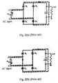
- a typical single-phase full-bridge rectifier is shown in Figs. 2(a) and (b) .
- the AC input can be a current source or a voltage source. In the first half cycle as shown in Fig. 2(a) , current flows through the input, diode D1, the load and diode D4, which is called a current loop.
- n-type power MOSFETs have lower on-state resistance than p-type MOSFETs, for high current applications, the two p-type MOSFETS mentioned previously can also be replaced by 2 n-type MOSFETS, provided that an extra inversion stage is added in the gate drive circuit as shown in Fig.4 in order to preserve the "self-driven" feature which is based on detecting the input ac power source.
- EP1056190 describes a power supply device, a power supply method, a portable electronic device, and an electronic watch.
- WO96/01003 describes a bridge rectifier circuit that uses active switches for at least two of its four rectifying elements, and employs an active control circuit to control the state of the active switches.
- US608792 describes a power converter that uses a switching signal having at least three levels of amplitude, one of which amplitude levels has a zero amplitude level during a predetermined switching interval.
- a rectifier configured to provide synchronous rectification when used in combination with either a current-source or a voltage-source, said rectifier comprising: a first circuit element (SX) coupled between a first input node and a first output node, a second circuit element (SX) coupled between a second input node and the first output node, a third circuit element (SX) coupled between a second output node and the first input node, the second and third circuit elements forming a first group, the first group being in a first current loop of the rectifier, a fourth circuit element (SX) coupled between the second output node and the second input node, the first and fourth circuit elements forming a second group, the second group being in a second current loop of the rectifier, the second current loop different from the first current loop; wherein at least one of the circuit elements is a first current-controlled active switch which is in the form of a self-driven current-controlled active switch comprising: an active switch (M1 - M4),
- the voltage- and current-controlled active switches are self-driven and do not require external control signals.
- One examples for such a voltage-controlled active switch is one that is driven by an input ac voltage provided to said switch by a gate drive circuit.
- An example of a current-controlled active switch is one that is driven by sensing the current direction of the switch and providing a signal to a gate drive circuit dependent on the current direction.
- An active switch may comprise a power MOSFET or some other semiconductor switching device.
- a sensing resistor may be used for sensing the current direction, including the possibility that the internal resistance of the current-controlled active switch may be used for sensing the current direction.
- the rectifier may be configured to receive a current source or a voltage source.
- each said branch comprising voltage- or current-controlled active switches, inductors, diodes or combinations thereof selected such that each said loop includes one active switch, inductor or diode from said upper branch and one active switch, inductor or diode from said lower branch, and wherein each said current loop comprises at least one diode, inductor or current-controlled active switch, and wherein at least one voltage- or current-controlled active switch is included in one of said upper or lower branches and with the proviso that no current loop may contain two inductors.
- the upper branch comprises two voltage-controlled active switches and the lower branch comprises two current-controlled active switches, or one current-controlled switch and one diode, or two diodes.
- the upper branch comprises one voltage-controlled active switch and one current-controlled active switch or diode
- the lower branch comprises one voltage-controlled active switch and one current-controlled active switch or diode, wherein the current-controlled active switch(es) or diode(s) are not provided in the same current loop.
- the upper branch comprises one voltage-controlled active switch and one current-controlled active switch or diode
- the lower branch comprises two current-controlled active switches, or one current-controlled switch and one diode, or two diodes.
- the upper branch comprises two current-controlled active switches, or one current-controlled switch and one diode, or two diodes
- the lower branch comprises two voltage-controlled active switches.
- the upper branch comprises two current-controlled active switches, or one current-controlled switch and one diode, or two diodes
- the lower branch comprises one voltage-controlled active switch and one current-controlled switch or one diode.
- the rectifier comprises only current-controlled active switches and/or diodes in the upper and lower branches and wherein at least one of the branches includes at least one current-controlled active switch.
- the rectifier is a half-bridge rectifier wherein the upper branch and the lower branch each comprises a capacitor and one of a current-controlled active switch, inductor or diode subject to the constraint that no more than one of the branches comprises a diode.
- a three-phase full-bridge rectifier comprising an upper branch and a lower branch and six current loops, each branch comprising voltage- or current-controlled active switches, diodes or combinations thereof selected such that each loop includes one active switch or diode from the upper branch and one active switch or diode from the lower branch, and wherein each the current loop comprises at least one diode or current-controlled active switch, and wherein at least one voltage- or current-controlled active switch is included in one of said upper or lower branches.
- the upper branch comprises three current-controlled active switches or diodes.
- the lower branch comprises three current-controlled active switches or diodes.
- the lower branch and the upper branch each comprise two current-controlled active switches or diodes, and each current loop comprises at least one current-controlled active switch or diode.
- each level includes at least one circuit topology comprising an upper branch and a lower branch and two current loops, and wherein at least said circuit topology is configured such that each said branch comprises voltage- or current-controlled active switches, inductors, diodes or combinations thereof selected such that each said loop includes one active switch, inductor or diode from said upper branch and one active switch, inductor or diode from said lower branch, and wherein each said current loop comprises at least one diode, inductor or current-controlled active switch, and wherein at least one voltage- or current-controlled active switch is included in one of said upper or lower branches and with the proviso that no current loop may contain two inductors.
- a current doubler comprising an upper branch and a lower branch and two current loops wherein the upper branch comprises two inductors, and the lower branch comprises voltage- or current-controlled active switches, diodes or combinations thereof, and the lower branch comprises at least one voltage-controlled active switch or at least one current-controlled active switch.
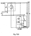
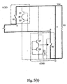
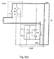
- Fig. 5(b) shows a second alternate implementation of CCSD active switch.
- the previous resistor Rsen shown in Fig. 5(a) has been removed.
- This CCSD active switch uses its internal resistance to detect the current flow direction.
- the comparator U1 can still produce the driving pulses according to the current flow direction detected by the internal active switch resistance.
- the driving pulse control mechanism for Q7 and Q8 is still the same as those in Fig. 5(a) .
- the advantage of this CCSD active switch is to eliminate the use of a sensing resistor.
- the drawback is that it may not be suitable for high voltage rectification as too high voltage at the sensing pin of comparator U1 would be inadequate.
- Fig. 5(c) shows a third alternate implementation of CCSD active switch.
- This CCSD active switch uses resistor Rsen for detecting the current flow direction of S4.
- the comparator U1 uses its non-inverting pin as the current sense detection pin.
- a voltage bias or level-shift voltage at the inverting pin, along with comparator's ground, being with reference to the "Source” of S4 (e.g. MOSFET acting as the active switch) is added.
- the positive current flow through S4 is detected by comparator U1 with the help of resistor Rsen.
- Positve driving pulse is then produced and the pulse control mechanism of Q7 and Q8 is preserved as shown in Fig. 5(a) .
- the addition of a bias voltage has reduced the turn-off delay time when reverse current occurring at the switch S4.
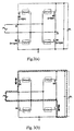
- Fig 3 shows one of the invalid SR configurations which has the problem of not blocking reverse current in a current loop of a rectifier. It is necessary to identify all valid SR circuits which are practical.
- a systematic way of SR identification is proposed and all possible SR circuits in rectification system will be tabulated accordingly.
- the circuit element (which can be an active switch, a diode, or other circuit element) in the upper branch is defined as SX i
- the circuit element in the lower branch is defined as, SX j where X represents the type of circuit element in the branch.
- a current-controlled self-driven (CCSD) active switch, a diode and an inductor have been associated with a logic value of "1". These types of circuit element show the capability of resisting instantaneous current change (while not being a switch in the conventional sense, an inductor can function successfully in embodiments of this invention as if it were a CCSD active switch as it is capable of resisting an instantaneous change in current direction - however it should be noted that a current loop comprising two inductors would not function).
- a voltage-controlled self-driven (VCSD) active switch and a capacitor have no such capability of resisting instantaneous current change. Therefore, they have been assigned a logic value of "0". Table 1 shows the corresponding logic value for each circuit element. Table 1 Logic assignments of different circuit elements X CCSD I Diode D Inductor L VCSD V capacitor C SX 1 1 1 0 0
- each current loop ⁇ X i , X j ⁇ can be identified by the branch location in the circuit and an associated circuit element in the branch can be mapped in the corresponding current loop.
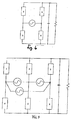
- circuit topologies which can contribute to the formation of an AC-DC self-driven synchronous rectification system are shown in the following figures, beginning with reference to Fig.6 and Table 1 which define the topology of a full-bridge rectifier and the associated current loops ⁇ 1,4 ⁇ , ⁇ 2,3 ⁇ where the upper branch comprises circuit elements 1 and 2, while the lower branch comprises circuit elements 3 and 4.
- Fig.7 and Table 2 illustrate the possible configurations for a half-bridge rectifier or voltage doubler, again with associated current loops ⁇ 1,4 ⁇ , ⁇ 2,3 ⁇ where the upper branch comprises circuit elements 1 and 2, and the lower branch comprises circuit elements 3 and 4.
- Fig.8 and Table 3 consider the situation of a current doubler with current loops ⁇ 1,4 ⁇ , ⁇ 2,3 ⁇ where the upper branch comprises circuit elements 1 and 2, and the lower branch comprises circuit elements 3 and 4, though in the case of the current doubler the upper branch, ie circuit elements 1 and 2, must comprise inductors L1 and L2.
- Fig. 9 and Table 4 considers a three-phase full-bridge rectifier with an upper branch comprising three circuit elements 1, 2 and 3, and a lower branch comprising three circuit elements 4, 5 and 6, with six associated current loops ⁇ 1,5 ⁇ ,1,6 ⁇ , ⁇ 2,4 ⁇ , ⁇ 2,6 ⁇ , ⁇ 3,4 ⁇ , ⁇ 3,5 ⁇ . From Table 4 it can be seen that there are 17 out of 56 valid configurations which have the function of self-driven synchronous rectification in the three-phase AC-DC rectifier system.
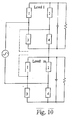
- Fig.10 and Table 6 considers a multi-level single-phase full-bridge rectifier system.
- the topology is that of a multi-level cascaded topology with two levels, but it will be understood that other configurations are possible.
- each level has two associated current loops ⁇ 1,4 ⁇ , ⁇ 2,3 ⁇ .
- the current flow in level 1 is independent of that in level m; therefore, the loop assignment and the associated circuit element in each branch are independent of the sub-level system they are in, and the benefits of the invention may be obtained provided that at least one level is structured such that there is at least one current-controlled active switch, inductor or diode in each current loop and that the level includes at least one voltage-controlled active switch or current-controlled active switch in one of the branches.
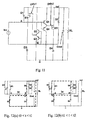
- a comparative example (which was initially indicated as a first embodiment of the invention) may take the form of a current-source input upper half VCSD full-bridge synchronous rectification (SR) as shown in Fig.11
- SR synchronous rectification
- M1 and M2 replace the upper diodes (D1 and D2 in Fig. 2 ) of the left and right branches of the diode-bridge.
- Dm1 and Dm2 can be either the body diode of the two MOSFETs or added external diodes.
- MOSFET M1 has its gate signal controlled by V B and MOSFET M2 has its gate signal controlled by voltage V A .
- Both MOSFET gates are cross-connected against the current-source input terminals (point A and point B) through the complementary gate drive circuits formed by the Q1-Q2 pair and Q3-Q4 pair.
- a gate drive buffer (totem poles, drivers or direct connection) between the current-source input and the MOSFETs can be used to drive the power switches to be ON/OFF accordingly.
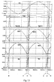
- Fig. 14 shows a simulated comparison of conduction losses between Schottky diodes used in Fig.2 and active switches (e.g. MOSFETs) used in Fig.11 .
- active switches e.g. MOSFETs
- FIG. 14 shows a simulated comparison of conduction losses between Schottky diodes used in Fig.2 and active switches (e.g. MOSFETs) used in Fig.11 .
- MOSFETs active switches
- the two active switches need not be turned off by sensing their reverse current and therefore may be either voltage-controlled or current-controlled active switches. But it must be stressed that the two diodes must be placed in either the upper half of the branches or the lower half of the branches. They must not be placed in the diagonal positions.
- a second embodiment of the invention (which now has become the first embodiment of the invention) comprises current-source input upper half VCSD and lower half current controlled self-driven' (CCSD) full-bridge synchronous rectification (SR) as shown in Fig. 15 .
- D3 and D4 in Fig. 5 are replaced with two n-type MOSFETs, M3 and M4, respectively.
- sensing resistors Rsen1 and Rsen2 are placed at both sides of the lower legs for detecting the current flow direction of M3 and M4 (defining positive current flow from ground up to Vout).
- Comparators U1 and U2 are used to produce driving pulses according to the current flow direction at Rsen1 and Rsen2.
- the voltage supplies of U1 and U2 can be directly derived from the rectified DC bulk voltage at the DC output, Vout, as this is the most cost effective method (or indirectly derived from an auxiliary power supply).
- a positive current through M3 and Dm3 or M4 and Dm4 will cause the output of comparator U1 or U2 go to high status.
- the high voltage level of the comparator output in turn, will drive the buffer Q5 or Q7 (totem pole or driver).
- Power switch M3 or M4 will be turned ON according to its positive current flow direction and it will be turned OFF in opposite manner.
- Two p-type MOSFETs are placed at the upper branch of the bridge, which form the upper half of the SD SR, and the gate drives use voltage control without reverse current sensing.
- This half period ends when the input current changes its current direction.
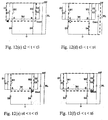
- M2 and M3 are still ON for a short period (t6 ⁇ t ⁇ t7).
- the reverse voltage developed at Rsen1 can cause the comparator U1 to flip over, latching buffer Q6.
- M3 is then OFF.
- M2 is still ON as V A is at a low state (t7 ⁇ t ⁇ t8).
- the reverse current flow discharges C1 of M1 in the path (M2, C1) and at the same time charges up C3 of M3 in the path (M2, C3, RL, Cout). In the process of rising to Vout, V A gradually reduces the negative threshold gate voltage of M2.
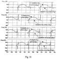
- Fig.18 shows a simulated comparison of conduction losses between Schottky diodes used in Fig.2 and active switches (e.g. MOSFETs) used in Fig.15 .
- active switches e.g. MOSFETs
- the simulation shows that the conduction loss of each Schottky diode (0.35V forward drop) contributes an average power loss of around 100mW in a cycle, while each active switch (e.g. MOSFET Si4403DY from Vishay, with 17mOhm ON-resistance) introduces an average loss of about 5mW.
- the comparative ratio is rather large on the order of ten.
- a third embodiment of the invention may take the form of voltage-source input upper half VCSD lower half CCSD full-bridge synchronous rectification as shown in Fig. 19 .
- the input of the proposed full-bridge SR can also be a voltage source, besides the current source in examples 1 and 2.
- a full version of voltage-source-input self-driven full-bridge SR is shown in Fig.19 .
- Sensing resistors Rsen1 and Rsen2 are placed at both the lower legs of the bridge for detecting the current flow direction (defining positive current flow from ground up to Vout).
- Comparator U1 and U2 are used to produce driving pulses according to the current flow direction at Rsen1 and Rsen2.
- a positive current at M3 and Dm3 or M4 and Dm4 will make output of comparator U1 or U2 go to high level.
- the high voltage level of the comparator in turn, will drive the buffer Q5 or Q7 (totem pole or driver).
- Power switch M3 or M4 will be turned ON according to its positive current flow direction and it will be turned OFF in opposite manner.
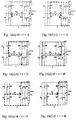
- Two p-type MOSFETs are at the upper branches of the bridge, which form the upper half VCSD SR. The operation of this application starts at t0. Input current flows from point A to point B in Fig.20 and Fig.21 . Both power MOSFETs M2 and M3 are ON. Voltage V B is at the level of Vout and voltage V A is at ground level (t0 ⁇ t ⁇ t1). This period finishes when the voltage V B is less than the output voltage Vout. The input source current keeps continuous flowing but changes its current direction in opposite way (t1 ⁇ t ⁇ t2).
- V B drops off.
- the fall of V B creates a negative threshold voltage for M1, which is then turning ON immediately.
- the input AC voltage is far less than the output voltage, Vout. No power is transferred to the output in this transition period (t4 ⁇ t ⁇ t5).
- V B Once the voltage V B is low enough to forward bias the diode Dm4 of M4 (t5 ⁇ t ⁇ t6).
- the positive current at Rsen2 will trigger the comparator U2 to go high.
- the output of U2 drives M4 to turn ON by the buffer Q7, and V A is higher than the output voltage. Power is delivered to the output instantaneously (t6 ⁇ t ⁇ t7).
- V B reaches the output voltage Vout (t9 ⁇ t ⁇ t10).
- C1 of M1 is being charged in the path (Dm2, C1) and C3 of M3 is being discharged in the path (Dm2, RL, Cout, C3).
- V A further drops off.
- the low voltage of V A also drive M2 into saturation through the buffer Q4 (t10 ⁇ t ⁇ t11).
- V A will reach the ground level and forward biasing the diode Dm3 of M3 in (t11 ⁇ t ⁇ t12). The cycle repeats after t12.
- the two current loops are diagonals, i.e. one loop comprises switches S1 and S4, and the other current loop comprises switches S3 and S4. If the switches are chosen from voltage-controlled self-driven active switches, current-controlled self-driven active switches and diodes, the critical requirement is that in each current loop there must be either a current-controlled active switch or a diode.
- the following table illustrates all the possible embodiments of the invention and in which 0 indicates a voltage-controlled active switch, and 1 indicates a current-controlled active switch or a diode.
- S1 S2 S3 S4 0 0 1 1 0 1 0 1 0 1 1 1 1 1 0 1 0 1 0 1 1 1 1 1 0 0 1 1 1 1 1 1 1 0 1 1 1 1 1
- each current loop i.e. S1 + S4 and S2 + S3
- a current-controlled active switch or a diode that will automatically switch off when the switch current direction is reversed.
- Embodiments of the present invention and in particular the embodiments with a voltage source input can be used in a utility power line (e.g. 110Vac, 220Vac, 50Hz, 60Hz, etc).
- a utility power line e.g. 110Vac, 220Vac, 50Hz, 60Hz, etc.
- the basic configurations of such power MOSFETs replacing diodes with the help of totem poles or drivers and the change of polarities of the voltage source facilitate AC power rectification for low and high power applications.
- a level shifter or any circuits with voltage scaling function
- Fig.22 is a single-phase AC-to-DC synchronous rectification system with 100-220Vac input, VCSD switches in the lower branch. Typical waveforms of the AC-to-DC lower half VCSD synchronous rectifier are shown in Fig.23 . Details of circuit operations are the same as AC-to-DC lower half VCSD synchronous rectifier with voltage-source input as shown in single-phase self-driven full-bridge synchronous rectification as described above.
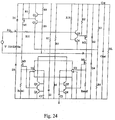
- Fig.24 shows a single-phase AC-to-DC synchronous rectification system with 110-220Vac input, CCSD switches in the lower branch and P-channel MOSFET VCSD switches in the upper branch.
- Fig. 25 shows the waveforms of the circuit in Fig.24 .
- the use of P-channel MOSFET in the upper branch has the advantage of ease of driving capability. However, the P-channel MOSFET still has higher turn-on resistance than that of N-channel MOSFET. For high power application multiple P-channel MOSFETs can be operated in parallel such that the equivalent turn-on resistance can be greatly reduced.
- the alternate approach is to use a N-channel MOSFET switch in the upper branch directly.
- Fig.26 shows a single-phase AC-to-DC synchronous rectification system with 110-220Vac input, CCSD switches in the lower branch and N-channel MOSFET VCSD switches in the upper branch.
- CCSD AC-to-DC synchronous rectification system
- N-channel MOSFET VCSD switches in the upper branch.
- D5, D6, Z1, Z2, R1, R2, R3 and R4 form two boost up circuits for switches M1 and M2 respectively.
- embodiments of the present invention can be implemented either using discrete electronic components, or as integrated circuits, and can be used to replace traditional diode rectifier circuits for applications from milli-watt to several tens of kilowatts.
- diode rectifier circuits for applications from milli-watt to several tens of kilowatts.
- there are many advantages including high compactness and reduction of heat-sink volume.
- traditional 1-phase full-bridge rectifier has conduction of around 20W - assuming 1V voltage drop across the diode and there are 4 diodes.
- the conduction loss is only 2W. This greatly reduces the power loss and so the heat-sink requirement is greatly reduced.
- the circuit can be integrated into a circuit block or independent modules.
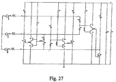
- FIG. 27 shows a three-phase voltage-source input lower half VCSD full-bridge synchronous rectification (SR) as shown in Fig. 27 .
- SR synchronous rectification
- the driving signal of each phase can be derived from its terminal voltages between adjacent phases through two-diode back-to-back connection or by some logical circuits which can provide logical function "AND” or “OR” functions. Therefore, the orientation of the diode depends on which branch (upper half or lower half) of the full-bridge rectifier it is required to drive. For lower half VCSD full-bridge SR the "AND” function should be employed. For upper half VCSD full-bridge SR the "OR” function should be employed. The absolute values of the derived signals (gate_ab, gate_bc, gate_ca) are then used to drive the buffers (totem poles or drivers) which are connected to the gates of the corresponding power MOSFETs.
- the signal flows can be shown logically as follows: Table 5 States of signal flows for driving a three-phase self-driven lower half VCSD full-bridge synchronous rectifier system with voltage-source input.
- Vcn > Vbn > Van, VC > VB, V(gate_bc) > 0, V(gate 4) > threshold of M4, M4 conducts, VA 0, (t4 ⁇ t ⁇ t5)
- VA 0.
- Vcn > Vbn > Van, VCA ⁇ Vd, D5 off, Vcn > Vbn, V(gate_bc) > 0, V(gate 4) > 0, M4 still conducts but I(M6) 0.
- VA 0.
- Vbn > Vcn > Van, VBA ⁇ Vd, D3 does not conduct yet, V(gate_bc) > 0, V(gate 4) > 0, M4 conducts, I(M4) 0.
- VA 0.
- Vbn Vcn > Van
- VBA Vd
- D3 off VC drops toward zero, C2 discharged
- VBC rises up
- V(gate_bc) 0,
- V(gate 4) 0, M4 still conducts, current flows reversely,
- Vgate4 reaches zero at the end of t8.
- Vbn Van > Vcn
- VBC ⁇ Vd
- D3 off VC reaches zero, D2 conducts, M4 off, VA increases.
- Vbn Van > Vcn, VBC ⁇ Vd, D3 off, V(gate_ac) > 0, V(gate 2) > threshold of M2, M2 conducts.
- Vbn Van > Vcn, VBC > Vd, D3 conducts, V(gate_ac) > 0, V(gate 2) > threshold of M2, M2 still conducts.
- I(M2) 0.
- VC 0.
- This comparative example may take the form of a multilevel voltage-source input lower half VCSD driven full-bridge synchronous rectification (SR).
- SR synchronous rectification
- Fig.29 shows a typical multi-level cascaded full-bridge rectifier system which employs a self-driven lower half VCSD with voltage-source input.
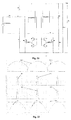
- Fig.30 shows the waveforms of a 2-level voltage-source input lower half VCSD full-bridge SR for demonstration.
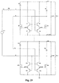
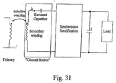
- FIG.31 An embodiment of an inductively powered secondary assembly including a synchronous rectification circuit is shown in Fig.31 .
- the secondary winding receives AC energy inductively from the energy transmitter (the primary) when it is placed on or in proximity with the transmitter.
- the current source and the full-bridge synchronous rectification have the same operation modes as described in example 1 or example 2. The decreased power loss due to the use of synchronous rectification can improve the efficiency of the inductive power transfer.
- the power loss due to the rectifier is reduced from 0.6-0.8W to less than 0.2W, because the internal resistance of each MOSFET is very low.
- Such saved loss is critical to the reduction of generated heat, especially when the secondary assembly is placed in any enclosed structure (e.g. in a mobile phone).
- the output of the secondary assembly can be used to power any DC load, like charging circuit for battery or for other energy storage component.
Landscapes
- Engineering & Computer Science (AREA)
- Power Engineering (AREA)
- Rectifiers (AREA)
Claims (5)
- Gleichrichter, der ausgelegt ist, um synchrone Gleichrichtung bereitzustellen, wenn er in Kombination mit entweder einer Stromquelle oder einer Spannungsquelle verwendet wird, wobei der Gleichrichter Folgendes umfasst:ein erstes Schaltungselement (SX), das zwischen einem ersten Eingangsknoten und einem ersten Ausgangsknoten gekoppelt ist;ein zweites Schaltungselement (SX), das zwischen einem zweiten Eingangsknoten und dem ersten Ausgangsknoten gekoppelt ist;ein drittes Schaltungselement (SX), das zwischen einem zweiten Ausgangsknoten und dem ersten Eingangsknoten gekoppelt ist, wobei das zweite und dritte Schaltungselement eine erste Gruppe bilden, wobei die erste Gruppe in einer ersten Stromschleife des Gleichrichters ist;ein viertes Schaltungselement (SX), das zwischen dem zweiten Ausgangsknoten und dem zweiten Eingangsknoten gekoppelt ist, wobei das erste und vierte Schaltungselement eine zweite Gruppe bilden, wobei die zweite Gruppe in einer zweiten Stromschleife des Gleichrichters ist, wobei sich die zweite Stromschleife von der ersten Stromschleife unterscheidet;wobei mindestens eines der Schaltungselemente ein erster stromgesteuerter aktiver Schalter ist, der in Form eines selbstgetriebenen stromgesteuerten aktiven Schalters ist, umfassend:einen aktiven Schalter (M1 - M4);einen Messwiderstand (Rsen, Rsen1, Rsen2) zum Messen einer Stromrichtung durch das Schaltungselement;eine Gate-Treiber-Schaltung zum Treiben des aktiven Schalters (M1-M4) basierend auf der gemessenen Stromrichtung; undeine erste Diode (D3, D4), die parallel mit dem aktiven Schalter und seriell mit dem Messwiderstand verbunden ist, um einem Strom zu erlauben, durch den Messwiderstand zu fließen, wenn der aktive Schalter in einem Aus-Zustand ist;wobei mindestens ein Schaltungselement von jeder der ersten und zweiten Gruppe eines aus der Gruppe ist, die aus einer Diode, einem Induktor und dem ersten und/oder einem zweiten stromgesteuerten aktiven Schalter besteht;wobei jedes andere Schaltungselement mindestens eines aus der Gruppe umfasst, die aus einer Diode, einem Induktor, einem Kondensator, einem spannungsgesteuerten aktiven Schalter, der durch ein Antriebsspannungssignal gesteuert wird, das auf einer Spannung basiert, die an dem Eingangsknoten angelegt ist, der nicht der Eingangsknoten, mit dem der stromgesteuerte aktive Schalter verbunden ist, oder einem weiteren stromgesteuerten Schalter besteht; undwobei, falls eine der ersten und zweiten Gruppe ein Schaltungselement aufweist, das ein Induktor ist, diese Gruppe eine Diode, einen Kondensator, einen der stromgesteuerten aktiven Schalter, den spannungsgesteuerten aktiven Schalter oder einen weiteren spannungsgesteuerten aktiven Schalter als anderes Schaltungselement in dieser Gruppe aufweist.
- Gleichrichter nach Anspruch 1, wobei der spannungsgesteuerte aktive Schalter durch eine Eingangswechselstromspannung getrieben wird, die dem Schalter durch eine Gate-Treiber-Schaltung bereitgestellt wird.
- Gleichrichter nach Anspruch 1, wobei der spannungsgesteuerte aktive Schalter einen Leistungs-MOSFET umfasst.
- Gleichrichter nach Anspruch 1, wobei jedes Schaltungselement ausgewählt ist aus der Gruppe, die nur aus stromgesteuerten aktiven Schaltern und Dioden besteht.
- Gleichrichter nach einem der vorhergehenden Ansprüche, wobei die erste Diode eine Body-Diode des aktiven Schalters ist.
Applications Claiming Priority (3)
| Application Number | Priority Date | Filing Date | Title |
|---|---|---|---|
| US12/194,921 US8942018B2 (en) | 2008-08-20 | 2008-08-20 | Single-phase self-driven full-bridge synchronous rectification |
| US12/274,469 US8711593B2 (en) | 2008-08-20 | 2008-11-20 | Generalized AC-DC synchronous rectification techniques for single- and multi-phase systems |
| PCT/CN2009/073355 WO2010020182A1 (en) | 2008-08-20 | 2009-08-19 | Generalized ac-dc synchronous rectification techniques for single- and multi-phase systems |
Publications (3)
| Publication Number | Publication Date |
|---|---|
| EP2321894A1 EP2321894A1 (de) | 2011-05-18 |
| EP2321894A4 EP2321894A4 (de) | 2013-05-15 |
| EP2321894B1 true EP2321894B1 (de) | 2016-07-13 |
Family
ID=41696236
Family Applications (1)
| Application Number | Title | Priority Date | Filing Date |
|---|---|---|---|
| EP09807881.9A Active EP2321894B1 (de) | 2008-08-20 | 2009-08-19 | Generalisierte synchrone ac-dc-gleichrichtungsverfahren für einzelphasensysteme |
Country Status (4)
| Country | Link |
|---|---|
| US (1) | US8711593B2 (de) |
| EP (1) | EP2321894B1 (de) |
| CN (1) | CN102246405B (de) |
| WO (1) | WO2010020182A1 (de) |
Cited By (1)
| Publication number | Priority date | Publication date | Assignee | Title |
|---|---|---|---|---|
| US10523036B2 (en) | 2016-12-14 | 2019-12-31 | Shenzhen Yichong Wireless Power Technology Co. Ltd | Resonant wireless charging system and method for electric toothbrush |
Families Citing this family (38)
| Publication number | Priority date | Publication date | Assignee | Title |
|---|---|---|---|---|
| US8614874B2 (en) * | 2005-11-22 | 2013-12-24 | Harris Corporation | Biased MOSFET active bridge with active gate drive |
| US8942018B2 (en) | 2008-08-20 | 2015-01-27 | ConvenientPower HK Ltd. | Single-phase self-driven full-bridge synchronous rectification |
| US8174214B2 (en) * | 2009-09-28 | 2012-05-08 | Harris Corporation | Three-phase low-loss rectifier with active gate drive |
| US8125808B2 (en) * | 2009-09-28 | 2012-02-28 | Harris Corporation | Three-phase low-loss rectifier |
| US8045350B2 (en) * | 2009-12-11 | 2011-10-25 | Harris Corporation | N-phase active bridge circuits including N-channel field effect transistors with active gate drive |
| US8913409B2 (en) | 2010-02-12 | 2014-12-16 | City University Of Hong Kong | Self-driven AC-DC synchronous rectifier for power applications |
| NZ587357A (en) | 2010-08-13 | 2013-03-28 | Auckland Uniservices Ltd | Control circuit for pick-up in inductive power transfer system selectively shunts diodes in rectifier bridge to reduce transient disturbances to primary current |
| US9024534B2 (en) * | 2010-10-04 | 2015-05-05 | Earl W. McCune, Jr. | Power conversion and control systems and methods for solid-state lighting |
| JP5658360B2 (ja) * | 2011-05-10 | 2015-01-21 | 三菱電機株式会社 | 直流電源装置および電力変換方法 |
| JP2013090415A (ja) * | 2011-10-17 | 2013-05-13 | Semiconductor Components Industries Llc | モータ駆動回路 |
| US9088222B2 (en) * | 2011-11-17 | 2015-07-21 | Qualcomm Incorporated | Systems, methods, and apparatus for a high power factor single phase rectifier |
| US9729081B1 (en) * | 2012-01-13 | 2017-08-08 | Maxim Integrated Products, Inc. | Powered device having semi-active bridge |
| US8804389B2 (en) * | 2012-02-16 | 2014-08-12 | Linear Technology Corporation | Active bridge rectification |
| DE102012203141A1 (de) * | 2012-02-29 | 2013-08-29 | Inficon Gmbh | Vorrichtung zur Spannungsversorgung der Kathode eines Massenspektrometers |
| CN102664551B (zh) * | 2012-05-11 | 2014-09-03 | 德州三和电器有限公司 | 自驱动工频同步换相全桥电路 |
| CN102790543B (zh) * | 2012-08-07 | 2015-10-14 | 浙江宇视科技有限公司 | 一种同步整流装置 |
| US9941813B2 (en) | 2013-03-14 | 2018-04-10 | Solaredge Technologies Ltd. | High frequency multi-level inverter |
| US9577546B2 (en) | 2013-03-15 | 2017-02-21 | Pai Capital Llc | Power converter with self-driven synchronous rectifier control circuitry |
| DE102013104944A1 (de) * | 2013-05-14 | 2014-11-20 | Endress + Hauser Gmbh + Co. Kg | Synchrongleichrichter, Verwendung eines solchen Synchrongleichrichters in einem Schaltnetzteil, sowie Schaltnetzteil |
| CN104426246B (zh) | 2013-09-04 | 2019-04-19 | 恩智浦美国有限公司 | 具有宽输入电压范围的无线电力发射器及其操作方法 |
| KR102120955B1 (ko) * | 2013-11-22 | 2020-06-10 | 삼성전자주식회사 | 시간 지연 기법을 이용하여 역전류 누설을 제거하는 역전류 보상 회로 및 능동형 정류기 |
| US9318974B2 (en) | 2014-03-26 | 2016-04-19 | Solaredge Technologies Ltd. | Multi-level inverter with flying capacitor topology |
| CN103916003A (zh) * | 2014-03-28 | 2014-07-09 | 上海交通大学 | 共阴极半桥功率因数校正电路 |
| CN103986345B (zh) * | 2014-04-30 | 2017-05-03 | 上海汇波智能控制设备有限公司 | 一种单、三相全电压电源转换器 |
| CN104092389B (zh) * | 2014-07-24 | 2016-09-07 | 国家电网公司 | 一种低损耗整流电路 |
| KR101670172B1 (ko) * | 2015-05-28 | 2016-10-28 | 삼성전기주식회사 | 정류 장치 |
| CN106877643B (zh) * | 2015-12-11 | 2019-09-03 | 华为技术有限公司 | 功率因数校正pfc电路及pfc电路的电压采样方法 |
| US9960608B2 (en) | 2016-03-04 | 2018-05-01 | Qualcomm Incorporated | High frequency multi-level rectification |
| SE540397C2 (en) * | 2016-11-25 | 2018-09-11 | Manetos Ab | Electric circuit with low voltage drop |
| JP6454800B2 (ja) * | 2018-02-07 | 2019-01-16 | ルネサスエレクトロニクス株式会社 | 半導体装置 |
| DE102018113146B4 (de) * | 2018-06-01 | 2020-02-06 | Infineon Technologies Ag | Gleichrichtereinrichtung und Halbleitereinrichtung |
| CN110912426B (zh) * | 2018-09-18 | 2023-04-07 | 上海峰飞航空科技有限公司 | 整流电路和直流功率生成电路 |
| US11418125B2 (en) | 2019-10-25 | 2022-08-16 | The Research Foundation For The State University Of New York | Three phase bidirectional AC-DC converter with bipolar voltage fed resonant stages |
| FR3104853B1 (fr) * | 2019-12-13 | 2022-08-19 | Commissariat Energie Atomique | Commande d'interrupteurs |
| CN111313730A (zh) * | 2019-12-26 | 2020-06-19 | 上海派能能源科技股份有限公司 | 一种mos管整流电路 |
| US20210281189A1 (en) * | 2020-03-03 | 2021-09-09 | Navitas Semiconductor Limited | Active bridge rectifier |
| CN113938035A (zh) * | 2020-07-14 | 2022-01-14 | 弗莱克斯有限公司 | 用于电源的设备、系统和方法 |
| KR102858579B1 (ko) * | 2020-09-10 | 2025-09-12 | 엘지이노텍 주식회사 | 브릿지리스 역률개선 컨버터 |
Family Cites Families (28)
| Publication number | Priority date | Publication date | Assignee | Title |
|---|---|---|---|---|
| US608792A (en) | 1898-08-09 | Apparatus for chemical cleaning | ||
| US4473757A (en) * | 1981-12-08 | 1984-09-25 | Intersil, Inc. | Circuit means for converting a bipolar input to a unipolar output |
| US4412277A (en) * | 1982-09-03 | 1983-10-25 | Rockwell International Corporation | AC-DC Converter having an improved power factor |
| US5303138A (en) * | 1993-04-29 | 1994-04-12 | At&T Bell Laboratories | Low loss synchronous rectifier for application to clamped-mode power converters |
| US5625541A (en) * | 1993-04-29 | 1997-04-29 | Lucent Technologies Inc. | Low loss synchronous rectifier for application to clamped-mode power converters |
| US5510972A (en) | 1994-06-29 | 1996-04-23 | Philips Electronics North America Corporation | Bridge rectifier circuit having active switches and an active control circuit |
| US6069799A (en) * | 1997-05-14 | 2000-05-30 | Lucent Technologies Inc. | Self-synchronized drive circuit for a synchronous rectifier in a clamped-mode power converter |
| US6011703A (en) * | 1997-07-30 | 2000-01-04 | Lucent Technologies Inc. | Self-synchronized gate drive for power converter employing self-driven synchronous rectifier and method of operation thereof |
| US6084792A (en) * | 1998-08-21 | 2000-07-04 | Vpt, Inc. | Power converter with circuits for providing gate driving |
| US6366485B1 (en) * | 1998-09-17 | 2002-04-02 | Seiko Epson Corporation | Power source device, power supplying method, portable electronic equipment, and electronic timepiece |
| US6091616A (en) * | 1998-10-21 | 2000-07-18 | Lucent Technologies Inc. | Drive compensation circuit for synchronous rectifier and method of operating the same |
| US6240318B1 (en) * | 1998-10-27 | 2001-05-29 | Richard P. Phillips | Transcutaneous energy transmission system with full wave Class E rectifier |
| US6038148A (en) * | 1998-12-11 | 2000-03-14 | Ericsson, Inc. | Self-driven synchronous rectification scheme |
| US6002597A (en) * | 1999-02-08 | 1999-12-14 | Lucent Technologies Inc. | Synchronous rectifier having dynamically adjustable current rating and method of operation thereof |
| US6301139B1 (en) * | 2000-04-06 | 2001-10-09 | Power-One, Inc. | Self-driven synchronous rectifier circuit for non-optimal reset secondary voltage |
| TW497327B (en) * | 2000-07-27 | 2002-08-01 | Wonderland Internat Inc | Simple flyback synchronous rectifier power supply |
| CN1144346C (zh) * | 2000-08-17 | 2004-03-31 | 伊博电源(杭州)有限公司 | 同步整流管的自驱动电路 |
| CN1169281C (zh) | 2001-04-10 | 2004-09-29 | 伊博电源(杭州)有限公司 | 低压输出同步整流管的自驱动电路 |
| US6563726B1 (en) * | 2001-11-21 | 2003-05-13 | Hewlett-Packard Company | Synchronous bridge rectifier |
| US6563719B1 (en) * | 2002-04-09 | 2003-05-13 | Bel-Fuse, Inc. | Self-driven synchronous rectification scheme |
| WO2004111759A2 (en) * | 2003-05-27 | 2004-12-23 | Purdue Research Foundation | Applied estimation of eigenvectors and eigenvalues |
| JP2005168276A (ja) | 2003-11-12 | 2005-06-23 | Sony Corp | スイッチング電源回路 |
| US7180762B2 (en) * | 2004-08-23 | 2007-02-20 | International Rectifier Corporation | Cascoded rectifier |
| US7495414B2 (en) * | 2005-07-25 | 2009-02-24 | Convenient Power Limited | Rechargeable battery circuit and structure for compatibility with a planar inductive charging platform |
| US7269038B2 (en) * | 2005-09-12 | 2007-09-11 | Fairchild Semiconductor Corporation | Vrms and rectified current sense full-bridge synchronous-rectification integrated with PFC |
| TWI278876B (en) * | 2006-01-03 | 2007-04-11 | Delta Electronics Inc | Transformer structure |
| FR2900292B1 (fr) | 2006-04-21 | 2008-11-14 | Airbus France Sas | Dispositif de securite pour interrupteur a semi-conducteurs |
| CN101154891B (zh) | 2006-09-28 | 2010-08-25 | 台达电子工业股份有限公司 | 谐振转换器及其同步整流驱动方法 |
-
2008
- 2008-11-20 US US12/274,469 patent/US8711593B2/en active Active
-
2009
- 2009-08-19 EP EP09807881.9A patent/EP2321894B1/de active Active
- 2009-08-19 CN CN200980132255.0A patent/CN102246405B/zh active Active
- 2009-08-19 WO PCT/CN2009/073355 patent/WO2010020182A1/en not_active Ceased
Cited By (1)
| Publication number | Priority date | Publication date | Assignee | Title |
|---|---|---|---|---|
| US10523036B2 (en) | 2016-12-14 | 2019-12-31 | Shenzhen Yichong Wireless Power Technology Co. Ltd | Resonant wireless charging system and method for electric toothbrush |
Also Published As
| Publication number | Publication date |
|---|---|
| EP2321894A4 (de) | 2013-05-15 |
| CN102246405B (zh) | 2016-06-08 |
| WO2010020182A1 (en) | 2010-02-25 |
| US20100046264A1 (en) | 2010-02-25 |
| EP2321894A1 (de) | 2011-05-18 |
| US8711593B2 (en) | 2014-04-29 |
| CN102246405A (zh) | 2011-11-16 |
Similar Documents
| Publication | Publication Date | Title |
|---|---|---|
| EP2321894B1 (de) | Generalisierte synchrone ac-dc-gleichrichtungsverfahren für einzelphasensysteme | |
| CN102124640B (zh) | 单相自驱动全桥同步整流 | |
| US9490694B2 (en) | Hybrid resonant bridgeless AC-DC power factor correction converter | |
| US7960950B2 (en) | Zero current switching | |
| CN102859855B (zh) | 用于高输入到输出电压转换的dc-dc变换器电路 | |
| US10199927B2 (en) | PWM scheme based on space vector modulation for three-phase rectifier converters | |
| CN101854120B (zh) | 一种高效率多功能反激变换器 | |
| US20120139505A1 (en) | Bridgeless PFC Converter and the Method Thereof | |
| US11223279B2 (en) | Resonant switched transformer converter | |
| US20100259240A1 (en) | Bridgeless PFC converter | |
| US20110292703A1 (en) | Single-stage AC-to-DC converter with isolation and power factor correction | |
| CN105144561B (zh) | Dc/dc转换器 | |
| US5057990A (en) | Bidirectional switching power apparatus with AC or DC output | |
| Siwakoti et al. | Power electronics converters—An overview | |
| US11108329B1 (en) | Switch-mode power supplies including three-level LLC circuits for low line and high line operation | |
| CN107346940A (zh) | 一种功率变换电路 | |
| CN103227575A (zh) | 三相软切换pfc整流器 | |
| US7944188B1 (en) | Power converter circuits having bipolar outputs and bipolar inputs | |
| CN106685242A (zh) | 单级交流至直流转换器 | |
| Lin et al. | New ZVS DC--DC converter with series-connected transformers to balance the output currents | |
| JP2002238257A (ja) | 共振型dc−dcコンバータの制御方法 | |
| Yoon et al. | Zero-voltage switching and soft-commutating two-transformer full-bridge PWM converter using the voltage-ripple | |
| CN203617925U (zh) | 用于电压转换器的电路和电压转换器以及包括该电路的斩波器 | |
| CN109995264B (zh) | 双向dc-ac变换器及其控制方法 | |
| US12301118B2 (en) | Forward mode soft switching power converter |
Legal Events
| Date | Code | Title | Description |
|---|---|---|---|
| PUAI | Public reference made under article 153(3) epc to a published international application that has entered the european phase |
Free format text: ORIGINAL CODE: 0009012 |
|
| 17P | Request for examination filed |
Effective date: 20110317 |
|
| AK | Designated contracting states |
Kind code of ref document: A1 Designated state(s): AT BE BG CH CY CZ DE DK EE ES FI FR GB GR HR HU IE IS IT LI LT LU LV MC MK MT NL NO PL PT RO SE SI SK SM TR |
|
| AX | Request for extension of the european patent |
Extension state: AL BA RS |
|
| DAX | Request for extension of the european patent (deleted) | ||
| A4 | Supplementary search report drawn up and despatched |
Effective date: 20130412 |
|
| RIC1 | Information provided on ipc code assigned before grant |
Ipc: H02M 7/219 20060101ALI20130408BHEP Ipc: H02M 3/335 20060101AFI20130408BHEP |
|
| 17Q | First examination report despatched |
Effective date: 20131205 |
|
| GRAP | Despatch of communication of intention to grant a patent |
Free format text: ORIGINAL CODE: EPIDOSNIGR1 |
|
| RIC1 | Information provided on ipc code assigned before grant |
Ipc: H03K 17/74 20060101ALI20160329BHEP Ipc: H03K 17/06 20060101ALI20160329BHEP Ipc: H03K 17/30 20060101ALI20160329BHEP Ipc: H02M 7/219 20060101AFI20160329BHEP |
|
| INTG | Intention to grant announced |
Effective date: 20160418 |
|
| GRAS | Grant fee paid |
Free format text: ORIGINAL CODE: EPIDOSNIGR3 |
|
| GRAA | (expected) grant |
Free format text: ORIGINAL CODE: 0009210 |
|
| REG | Reference to a national code |
Ref country code: FR Ref legal event code: PLFP Year of fee payment: 8 |
|
| AK | Designated contracting states |
Kind code of ref document: B1 Designated state(s): AT BE BG CH CY CZ DE DK EE ES FI FR GB GR HR HU IE IS IT LI LT LU LV MC MK MT NL NO PL PT RO SE SI SK SM TR |
|
| REG | Reference to a national code |
Ref country code: GB Ref legal event code: FG4D |
|
| REG | Reference to a national code |
Ref country code: AT Ref legal event code: REF Ref document number: 813012 Country of ref document: AT Kind code of ref document: T Effective date: 20160715 Ref country code: CH Ref legal event code: EP |
|
| REG | Reference to a national code |
Ref country code: IE Ref legal event code: FG4D |
|
| REG | Reference to a national code |
Ref country code: DE Ref legal event code: R096 Ref document number: 602009039741 Country of ref document: DE |
|
| REG | Reference to a national code |
Ref country code: LT Ref legal event code: MG4D |
|
| REG | Reference to a national code |
Ref country code: NL Ref legal event code: MP Effective date: 20160713 |
|
| REG | Reference to a national code |
Ref country code: AT Ref legal event code: MK05 Ref document number: 813012 Country of ref document: AT Kind code of ref document: T Effective date: 20160713 |
|
| PG25 | Lapsed in a contracting state [announced via postgrant information from national office to epo] |
Ref country code: BE Free format text: LAPSE BECAUSE OF NON-PAYMENT OF DUE FEES Effective date: 20160831 |
|
| PG25 | Lapsed in a contracting state [announced via postgrant information from national office to epo] |
Ref country code: IS Free format text: LAPSE BECAUSE OF FAILURE TO SUBMIT A TRANSLATION OF THE DESCRIPTION OR TO PAY THE FEE WITHIN THE PRESCRIBED TIME-LIMIT Effective date: 20161113 Ref country code: HR Free format text: LAPSE BECAUSE OF FAILURE TO SUBMIT A TRANSLATION OF THE DESCRIPTION OR TO PAY THE FEE WITHIN THE PRESCRIBED TIME-LIMIT Effective date: 20160713 Ref country code: IT Free format text: LAPSE BECAUSE OF FAILURE TO SUBMIT A TRANSLATION OF THE DESCRIPTION OR TO PAY THE FEE WITHIN THE PRESCRIBED TIME-LIMIT Effective date: 20160713 Ref country code: LT Free format text: LAPSE BECAUSE OF FAILURE TO SUBMIT A TRANSLATION OF THE DESCRIPTION OR TO PAY THE FEE WITHIN THE PRESCRIBED TIME-LIMIT Effective date: 20160713 Ref country code: FI Free format text: LAPSE BECAUSE OF FAILURE TO SUBMIT A TRANSLATION OF THE DESCRIPTION OR TO PAY THE FEE WITHIN THE PRESCRIBED TIME-LIMIT Effective date: 20160713 Ref country code: NO Free format text: LAPSE BECAUSE OF FAILURE TO SUBMIT A TRANSLATION OF THE DESCRIPTION OR TO PAY THE FEE WITHIN THE PRESCRIBED TIME-LIMIT Effective date: 20161013 Ref country code: NL Free format text: LAPSE BECAUSE OF FAILURE TO SUBMIT A TRANSLATION OF THE DESCRIPTION OR TO PAY THE FEE WITHIN THE PRESCRIBED TIME-LIMIT Effective date: 20160713 |
|
| PG25 | Lapsed in a contracting state [announced via postgrant information from national office to epo] |
Ref country code: SE Free format text: LAPSE BECAUSE OF FAILURE TO SUBMIT A TRANSLATION OF THE DESCRIPTION OR TO PAY THE FEE WITHIN THE PRESCRIBED TIME-LIMIT Effective date: 20160713 Ref country code: LV Free format text: LAPSE BECAUSE OF FAILURE TO SUBMIT A TRANSLATION OF THE DESCRIPTION OR TO PAY THE FEE WITHIN THE PRESCRIBED TIME-LIMIT Effective date: 20160713 Ref country code: AT Free format text: LAPSE BECAUSE OF FAILURE TO SUBMIT A TRANSLATION OF THE DESCRIPTION OR TO PAY THE FEE WITHIN THE PRESCRIBED TIME-LIMIT Effective date: 20160713 Ref country code: PL Free format text: LAPSE BECAUSE OF FAILURE TO SUBMIT A TRANSLATION OF THE DESCRIPTION OR TO PAY THE FEE WITHIN THE PRESCRIBED TIME-LIMIT Effective date: 20160713 Ref country code: BE Free format text: LAPSE BECAUSE OF FAILURE TO SUBMIT A TRANSLATION OF THE DESCRIPTION OR TO PAY THE FEE WITHIN THE PRESCRIBED TIME-LIMIT Effective date: 20160713 Ref country code: ES Free format text: LAPSE BECAUSE OF FAILURE TO SUBMIT A TRANSLATION OF THE DESCRIPTION OR TO PAY THE FEE WITHIN THE PRESCRIBED TIME-LIMIT Effective date: 20160713 Ref country code: GR Free format text: LAPSE BECAUSE OF FAILURE TO SUBMIT A TRANSLATION OF THE DESCRIPTION OR TO PAY THE FEE WITHIN THE PRESCRIBED TIME-LIMIT Effective date: 20161014 Ref country code: PT Free format text: LAPSE BECAUSE OF FAILURE TO SUBMIT A TRANSLATION OF THE DESCRIPTION OR TO PAY THE FEE WITHIN THE PRESCRIBED TIME-LIMIT Effective date: 20161114 |
|
| REG | Reference to a national code |
Ref country code: CH Ref legal event code: PL |
|
| REG | Reference to a national code |
Ref country code: DE Ref legal event code: R097 Ref document number: 602009039741 Country of ref document: DE |
|
| PG25 | Lapsed in a contracting state [announced via postgrant information from national office to epo] |
Ref country code: CH Free format text: LAPSE BECAUSE OF NON-PAYMENT OF DUE FEES Effective date: 20160831 Ref country code: RO Free format text: LAPSE BECAUSE OF FAILURE TO SUBMIT A TRANSLATION OF THE DESCRIPTION OR TO PAY THE FEE WITHIN THE PRESCRIBED TIME-LIMIT Effective date: 20160713 Ref country code: LI Free format text: LAPSE BECAUSE OF NON-PAYMENT OF DUE FEES Effective date: 20160831 Ref country code: MC Free format text: LAPSE BECAUSE OF FAILURE TO SUBMIT A TRANSLATION OF THE DESCRIPTION OR TO PAY THE FEE WITHIN THE PRESCRIBED TIME-LIMIT Effective date: 20160713 Ref country code: EE Free format text: LAPSE BECAUSE OF FAILURE TO SUBMIT A TRANSLATION OF THE DESCRIPTION OR TO PAY THE FEE WITHIN THE PRESCRIBED TIME-LIMIT Effective date: 20160713 |
|
| PLBE | No opposition filed within time limit |
Free format text: ORIGINAL CODE: 0009261 |
|
| STAA | Information on the status of an ep patent application or granted ep patent |
Free format text: STATUS: NO OPPOSITION FILED WITHIN TIME LIMIT |
|
| PG25 | Lapsed in a contracting state [announced via postgrant information from national office to epo] |
Ref country code: SK Free format text: LAPSE BECAUSE OF FAILURE TO SUBMIT A TRANSLATION OF THE DESCRIPTION OR TO PAY THE FEE WITHIN THE PRESCRIBED TIME-LIMIT Effective date: 20160713 Ref country code: SM Free format text: LAPSE BECAUSE OF FAILURE TO SUBMIT A TRANSLATION OF THE DESCRIPTION OR TO PAY THE FEE WITHIN THE PRESCRIBED TIME-LIMIT Effective date: 20160713 Ref country code: BG Free format text: LAPSE BECAUSE OF FAILURE TO SUBMIT A TRANSLATION OF THE DESCRIPTION OR TO PAY THE FEE WITHIN THE PRESCRIBED TIME-LIMIT Effective date: 20161013 Ref country code: CZ Free format text: LAPSE BECAUSE OF FAILURE TO SUBMIT A TRANSLATION OF THE DESCRIPTION OR TO PAY THE FEE WITHIN THE PRESCRIBED TIME-LIMIT Effective date: 20160713 Ref country code: DK Free format text: LAPSE BECAUSE OF FAILURE TO SUBMIT A TRANSLATION OF THE DESCRIPTION OR TO PAY THE FEE WITHIN THE PRESCRIBED TIME-LIMIT Effective date: 20160713 |
|
| REG | Reference to a national code |
Ref country code: IE Ref legal event code: MM4A |
|
| 26N | No opposition filed |
Effective date: 20170418 |
|
| REG | Reference to a national code |
Ref country code: FR Ref legal event code: PLFP Year of fee payment: 9 |
|
| PG25 | Lapsed in a contracting state [announced via postgrant information from national office to epo] |
Ref country code: IE Free format text: LAPSE BECAUSE OF NON-PAYMENT OF DUE FEES Effective date: 20160819 |
|
| PG25 | Lapsed in a contracting state [announced via postgrant information from national office to epo] |
Ref country code: LU Free format text: LAPSE BECAUSE OF NON-PAYMENT OF DUE FEES Effective date: 20160819 Ref country code: SI Free format text: LAPSE BECAUSE OF FAILURE TO SUBMIT A TRANSLATION OF THE DESCRIPTION OR TO PAY THE FEE WITHIN THE PRESCRIBED TIME-LIMIT Effective date: 20160713 |
|
| PG25 | Lapsed in a contracting state [announced via postgrant information from national office to epo] |
Ref country code: CY Free format text: LAPSE BECAUSE OF FAILURE TO SUBMIT A TRANSLATION OF THE DESCRIPTION OR TO PAY THE FEE WITHIN THE PRESCRIBED TIME-LIMIT Effective date: 20160713 Ref country code: HU Free format text: LAPSE BECAUSE OF FAILURE TO SUBMIT A TRANSLATION OF THE DESCRIPTION OR TO PAY THE FEE WITHIN THE PRESCRIBED TIME-LIMIT; INVALID AB INITIO Effective date: 20090819 |
|
| PG25 | Lapsed in a contracting state [announced via postgrant information from national office to epo] |
Ref country code: TR Free format text: LAPSE BECAUSE OF FAILURE TO SUBMIT A TRANSLATION OF THE DESCRIPTION OR TO PAY THE FEE WITHIN THE PRESCRIBED TIME-LIMIT Effective date: 20160713 Ref country code: MT Free format text: LAPSE BECAUSE OF NON-PAYMENT OF DUE FEES Effective date: 20160831 Ref country code: MK Free format text: LAPSE BECAUSE OF FAILURE TO SUBMIT A TRANSLATION OF THE DESCRIPTION OR TO PAY THE FEE WITHIN THE PRESCRIBED TIME-LIMIT Effective date: 20160713 |
|
| REG | Reference to a national code |
Ref country code: FR Ref legal event code: PLFP Year of fee payment: 10 |
|
| PGFP | Annual fee paid to national office [announced via postgrant information from national office to epo] |
Ref country code: DE Payment date: 20250826 Year of fee payment: 17 |
|
| PGFP | Annual fee paid to national office [announced via postgrant information from national office to epo] |
Ref country code: GB Payment date: 20250825 Year of fee payment: 17 |
|
| PGFP | Annual fee paid to national office [announced via postgrant information from national office to epo] |
Ref country code: FR Payment date: 20250826 Year of fee payment: 17 |