EP2321901B1 - Hybrid-klasse-verstärker - Google Patents
Hybrid-klasse-verstärker Download PDFInfo
- Publication number
- EP2321901B1 EP2321901B1 EP08813476.2A EP08813476A EP2321901B1 EP 2321901 B1 EP2321901 B1 EP 2321901B1 EP 08813476 A EP08813476 A EP 08813476A EP 2321901 B1 EP2321901 B1 EP 2321901B1
- Authority
- EP
- European Patent Office
- Prior art keywords
- class
- power amplifier
- amplifier
- transistor
- output
- Prior art date
- Legal status (The legal status is an assumption and is not a legal conclusion. Google has not performed a legal analysis and makes no representation as to the accuracy of the status listed.)
- Active
Links
Images










Classifications
-
- H—ELECTRICITY
- H03—ELECTRONIC CIRCUITRY
- H03F—AMPLIFIERS
- H03F3/00—Amplifiers with only discharge tubes or only semiconductor devices as amplifying elements
- H03F3/04—Amplifiers with only discharge tubes or only semiconductor devices as amplifying elements with semiconductor devices only
- H03F3/16—Amplifiers with only discharge tubes or only semiconductor devices as amplifying elements with semiconductor devices only with field-effect devices
-
- H—ELECTRICITY
- H03—ELECTRONIC CIRCUITRY
- H03F—AMPLIFIERS
- H03F1/00—Details of amplifiers with only discharge tubes, only semiconductor devices or only unspecified devices as amplifying elements
- H03F1/02—Modifications of amplifiers to raise the efficiency, e.g. gliding Class A stages, use of an auxiliary oscillation
- H03F1/0205—Modifications of amplifiers to raise the efficiency, e.g. gliding Class A stages, use of an auxiliary oscillation in transistor amplifiers
-
- H—ELECTRICITY
- H03—ELECTRONIC CIRCUITRY
- H03F—AMPLIFIERS
- H03F1/00—Details of amplifiers with only discharge tubes, only semiconductor devices or only unspecified devices as amplifying elements
- H03F1/56—Modifications of input or output impedances, not otherwise provided for
-
- H—ELECTRICITY
- H03—ELECTRONIC CIRCUITRY
- H03F—AMPLIFIERS
- H03F3/00—Amplifiers with only discharge tubes or only semiconductor devices as amplifying elements
- H03F3/189—High-frequency amplifiers, e.g. radio frequency amplifiers
- H03F3/19—High-frequency amplifiers, e.g. radio frequency amplifiers with semiconductor devices only
-
- H—ELECTRICITY
- H03—ELECTRONIC CIRCUITRY
- H03F—AMPLIFIERS
- H03F3/00—Amplifiers with only discharge tubes or only semiconductor devices as amplifying elements
- H03F3/20—Power amplifiers, e.g. Class B amplifiers, Class C amplifiers
- H03F3/21—Power amplifiers, e.g. Class B amplifiers, Class C amplifiers with semiconductor devices only
- H03F3/217—Class D power amplifiers; Switching amplifiers
Definitions
- the present invention generally relates to an amplifier capable of operating in different class modes and, more particularly, to mechanisms and techniques for configuring an amplifier to have selected features of a class C amplifier and selected features of a class F or inverse class F amplifier.
- the rapid growth of mobile telecommunications services has created increasing demand for low-cost, low-power and reduced size and weight equipment.
- One such equipment is found in the transmitters in base stations and terminals for mobile telephony, as well as transmitters for broadcast and other wireless systems.
- the transmitters employ power amplifiers to amplify a radio frequency (RF) signal to the antenna.
- RF radio frequency
- the power amplifier needs to be highly efficient, to not overheat, require excessive cooling or draw less power to increase battery time and decrease the cost of power.
- One aspect of amplifier efficiency is related to the current and voltage waveforms used by the power amplifier. More specifically, the amplifier efficiency is related to an amount of simultaneous voltage drop over, and current through, a transistor that is part of the power amplifier. A reduction in the voltage drop and current through the transistor results in a reduction in the used power. The reduction in voltage drop and the current through the transistor are indicated by the waveforms of the current and voltage at the transistor.
- the optimal waveforms for high (maximum) output power are different from the waveforms at low output powers (relative maximum output), and the traditional circuits used for obtaining those waveforms are mutually exclusive.
- power amplifiers are categorized into different classes according to their linearity and the waveforms for current and voltage.
- the two major classes of power amplifiers are linear and non-linear power amplifiers.
- Classes A, AB, B and C correspond to linear power amplifiers while classes D and F correspond to non-linear power amplifiers.
- Figure 1A shows the output of a linear power amplifier
- Figure 1B shows the output of a non-linear power amplifier.
- the axes of Figures 1A and B use arbitrary units.
- Classes A, AB, B, C, D and F are discussed next in more detail.
- Each class is characterized by circuit properties (which are the same for some classes) and a bias applied to the transistor (which may be different between some classes).
- a class A power amplifier is defined as an amplifier that is biased so that the output current flows all the time, as shown in Figure 2 , and the input signal drive level is kept small enough to avoid driving the transistor in the cut-off region.
- a conduction angle of the transistor is 360°, meaning that the transistor conducts for the full cycle of the input signal. This property makes the class A power amplifier the most linear of all the amplifier types.
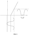
- a class B power amplifier is an amplifier in which the conduction angle for the transistor is approximately 180°, as shown in Figure 3 .
- the current waveform is a half-wave rectified sinewave and the voltage is confined by a parallel resonant tank circuit to be a sine offset by the supply voltage.
- Ideal transistors for class B operation have constant transconductance above cut-off and the gate or base biased right at the cut-off.
- the direct current (DC) supply current is then directly proportional to the RF output current (i.e., to the fundamental harmonic component of the half-wave rectified sine).
- the sinusoidal RF output voltage is also proportional to the RF output current (for the common linear load resistance). This in turn makes the efficiency of the power amplifier proportional to the output signal's amplitude.
- the efficiency of the constant supply voltage class B amplifier is proportional to the output voltage, up to a maximum of 78.5% for ideal devices in a lossless circuit.
- the average efficiency for a class B amplifier, outputting a signal whose average signal level is low compared to the maximum (peak) level, i.e., that has a high peak-to-average ratio, is therefore low compared to the efficiency at a maximum output.
- quadsi-linear do not have constant transconductance above cut-off, but can be seen as having a first substantially linear part followed by a substantially constant part (above which it usually drops off again).
- class AB bias so called class AB bias, shown in Figure 4 .
- a constant (DC) bias voltage applied to the gate or base is chosen as the point on the transconductance slope around which the transconductance is maximally (odd) symmetric. In the simplified model shown in Figure 4 , this point is exactly in the middle of the linear slope part of the transconductance curve.
- the current pulses of the class AB power amplifier are similar to the half-wave rectified sinewave pulses of class B but complemented with "tails" on each side.
- the output response is nonlinear with respect to the input.
- the efficiency is thus better than for the ideal class B amplifier, but the maximum output is lower (for otherwise equal conditions).
- the current waveform consists of narrower pulses than for ideal class B or AB power amplifiers, which indicates a greater content of higher harmonics.
- the class C power amplifier is an amplifier in which the conduction angle for the transistor may be less than 180° and the characteristic output of this amplifier is shown in Figure 5 .
- the class C power amplifier is characterized by having narrow output current pulses at a transistor of the power amplifier.
- class A power amplifier By increasing the gate bias above class AB, to the point that the current is continuously drawn even at high amplitudes, a class A power amplifier is obtained.
- This class has low efficiency for small signals, since the DC supply current drawn is high and largely independent of the signal level.
- the class A power amplifiers are used, inspite of the low efficiency, because they have a higher gain than other classes, which makes it possible to reach a maximum output with a small drive amplifier.
- the maximum RF output current of class A amplifiers may be larger than for class B or AB power amplifiers, for the same limitation in instantaneous drain (collector or, more generally, the active device's output node) current.
- the maximum output power can be increased.
- the abovementioned classes of operation may be obtained by a same circuit, which is characterized by a RF tank (parallel resonator at the fundamental frequency in parallel with the load).
- the RF tank is necessary because in coupling a tuned RF power amplifier to its load (the antenna or antenna feed line), the correct load resistance, which will enable the amplifier to deliver its rated power, has to be present to the output of the power amplifier.
- the RF tank ensures that this condition is fulfilled by shorting the harmonics of the current waveform, thereby forcing the output voltage to be sinusoidal.
- Other functions of the output circuit are to provide the DC current to the transistor through the RF choke and to block the DC from the supply voltage from reaching the load. Since the circuits for the above classes are identical, the difference between these classes of operation lies in the difference in current waveforms, which is caused by different (DC) gate biases to the transistor.
- Non-linear amplifiers include class D and class F amplifiers and these amplifiers will be discussed later in more detail.
- An increase in the maximum power and efficiency relative to the linear amplifiers may be achieved by the class F and inverse F type amplifiers.
- the class F and inverse F amplifiers are characterized by a square-shaped output voltage waveform at a transistor of the power amplifier.
- the effect of class F/inverse F is to obtain a more square-shaped voltage or current waveform as described in V. J. Tyler, "A new high efficiency high power amplifier", Marconi Review, vol. 21, no. 130, pp 96-109 , Third Quarter 1958 and F. H. Raab, "Maximum efficiency and output of class-F power amplifiers", IEEE trans. MTT, vol. 49, no. 6, June 2001 .
- a voltage-switching class D power amplifier corresponds to a class F power amplifier and a current-switching class D power amplifier corresponds to an inverse class F power amplifier.
- the transistor output of the power amplifier "sees" a high impedance (ideally an open circuit) at odd harmonic frequencies instead of short circuits at all harmonics, then a class F power amplifier is present.
- the high impedance for the odd harmonic frequencies may be obtained by inserting parallel resonators ("harmonic block") in series with the previously described harmonically shorted load (tank and load).
- the class F power amplifier may have a high impedance at odd harmonics (often only the third). Instead, if some even harmonics (often only the second) "see” a high impedance, then an inverse class F power amplifier is present. If more harmonics are to have the high impedance, more parallel resonators are inserted in series, while keeping the remaining harmonics shorted.
- the thus flattened waveform has a higher fundamental (RF) amplitude than the peak voltage or current would otherwise allow. This is due to the odd (voltage or current) harmonics that are in antiphase with the fundamental (voltage or current) at its peak, thus suppressing the peak without reducing the fundamental (i.e., flattening the wave towards a more square-shaped form).
- the high harmonic impedance caused by the parallel resonators imply that even a small harmonic current due to the current pulse shape causes a large voltage. This process is self-regulating in the maximum amplitude region due to the instantaneous current reduction due to voltage saturation ("I-V curve behaviour").
- the class BD amplifier uses linear class B operation at low and medium amplitudes, but increases the maximum output power by using current-switching class D.
- the class BD amplifier is described in F. H. Raab, "The class BD high-efficiency RF power amplifier", IEEE Journal of Solid-State Circuits, vol. SC-12, no. 3, June 1977 .
- the class BD power amplifier does not use class C or dynamic gate biasing.
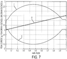
- Figure 7 shows the maximum and minimum drain voltages versus amplitude for the power amplifier. This figure shows an amplitude sweep of a class F amplifier with dynamic class C excitation. There are large voltage overshoots (r) and undershoots (b) at all amplitudes except the extreme low and high.
- a reconfigurable power amplifier includes at least one amplification circuit (E1,E2), and a circuit (6) for controlling the amplification circuit so as to adapt its operation according to an applied input signal (RFin).
- the circuit for controlling includes a circuit (4, 5) for modifying the compression point of the amplification circuit and for adapting the gain of the amplification circuit in such a manner as to increase the power added efficiency of the circuit for the modified compression point.
- a power amplifier configured to generate impedances at harmonic frequencies such that the power amplifier operates in a class C mode in a low output amplitude range and in a class F or inverse class F mode in a high output amplitude range according to claim 1.
- the method includes generating impedances at harmonic frequencies such that the power amplifier operates in a class C mode in a low output amplitude range and in a class F or inverse class F mode in a high output amplitude range.
- a novel amplifier may include smaller (and therefore cheaper) transistors to be used for the same maximum output power and may have a higher average efficiency for signals with a high peak to average ratio, due to the increase in the maximum output power for a given transistor.
- This novel configuration may move the high efficiency region of class C operation towards lower amplitudes (where the typical multicarrier signal is most of the time present).
- a novel amplifier according to another exemplary embodiment may increase the output power above that of a class F power amplifier while retaining the high average efficiency associated with the class F power amplifier.
- novel power amplifiers discussed in the following exemplary embodiments are applicable to, for example, linear transmitters for multi-carrier/multi-user radio signals (Code Division Multiple Access (CDMA), Orthogonal Frequency-Division Multiplexing (OFDM), and Frequency Division Multiple Access (FDMA)).
- CDMA Code Division Multiple Access
- OFDM Orthogonal Frequency-Division Multiplexing
- FDMA Frequency Division Multiple Access
- the term “narrow current pulses” may be used in some exemplary embodiments to define a class C amplifier.
- the class C amplifier which is know in the literature and well defined, includes a definition of the underlying circuit, which is not compatible with applying narrow pulses to a modified class F circuit.
- the term “narrow current pulses” is used, according to an exemplary embodiment, to define current pulses that are narrower than what a regular class F amplifier would handle.
- the term “narrow current pulses” does not include a specific circuit. However, this definition is not a general definition but may vary from case to case, for example from transistor to transistor.
- the novel power amplifier By introducing a resistance or an impedance that is seen, at the harmonic frequency or frequencies, by the transistor as relatively close in magnitude to the (transformed) load instead of having a high impedance as in a class F power amplifier, the novel power amplifier retains both the capability of high output power and the increased efficiency of (variable) class C operation at medium output amplitudes.
- the harmonic resistance degrades the efficiency at the highest output amplitudes, but not at low and medium amplitudes. For general multi-carrier/multiuser radio signals (CDMA, OFDM, FDMA), this is often not a problem, because the signals in these systems are rarely in the maximum amplitude region.
- a power amplifier 10 may include a transistor 12 (drive signal and dynamic gate bias circuitry omitted) having a supply voltage Vdd fed through an RF choke (inductor) 14, a DC blocking capacitor 16 that blocks a direct current component from reaching a load, and an output circuit 18 that has specific impedances for different harmonic overtones, as will be discussed next.
- the output circuit 18 blocks the harmonics produced by the transistor 12, by using at least one parallel resonator 20 and one or more series resonators 22, 24 and 26, from reaching a load 28.
- the series resonators 22 and 24 provide short circuits at overtone frequencies 2 x fc and 4 x fc (where fc is the fundamental frequency).
- the interaction between the parallel coupled series resonators 22 and 24 produces high impedance values for the odd harmonics, for example for the third harmonic.
- the impedance at the odd harmonics is reduced by the resistor 30, which is marked "R Term .”
- the resistor 30 is blocked at the fundamental frequency fc by the parallel resonator 20.
- the resistor 30, has a value close to that of the resistance of the resistor 28, which is marked "R Load " at odd frequencies.
- the impedance may also be different for different (odd) overtones, for example decreasing with frequency.
- a capacitor 44 may be added in parallel with the series resonators 22, 24, and 26 to act as a short circuit at infinity to terminate higher harmonics and to cause another odd harmonic resonance.
- the parallel resonator 20 includes a resistor 30.
- the resistor 30 may be connected in series with a capacitor 32 and an inductor 34, where the capacitor 32 and the inductor 34 are connected in parallel.
- the series resonator 22 may include a capacitor 36 connected in series with an inductor 38.
- the series resonator 24 may include a capacitor 40 connected in series with an inductor 42.
- the series resonator 26 may include a capacitor 44 connected in series to the inductor 48.
- the capacitances and inductances for the above discussed parallel and series resonators depend on the characteristics of the transistor and other elements used in the power amplifier.
- the series resonators 22 and 24 are connected together with the parallel resonator 20 in parallel between an emitter and a collector of the transistor 12 while the series resonator 26 may be connected between the emitter of the transistor 10 and the R Load 28.
- the output circuit 18 may include only the resistor R Term , one series resonator 22 or 24 and the capacitor 46.
- This arrangement provides a resistive third harmonic and shorted second and fourth to infinity frequencies.
- more series resonators for different even harmonics
- a similar behaviour may be obtained by an infinite number of circuits.
- "microwave circuit” techniques i.e., distributed elements, lines, etc.
- Other ways to build class F amplifiers may be used if complemented with resistive termination that is seen only at the harmonics, i.e., isolated from the rest of the circuit at the fundamental frequency.
- Figure 9 shows the impedance frequency response "A” as seen by the transistor output (drain) for the exemplary circuit shown in Figure 8 , the impedance frequency response "B” for using the circuit of Figure 8 with a larger R term , and the impedance frequency response "C” for a reference class F amplifier.
- the frequency response "C” of the reference class F amplifier is much larger than the frequency responses "A” and "B” of the exemplary embodiments.
- the voltage outside the current pulse which is not self-regulated by the saturation (I-V) behaviour of the transistor, may be made less than that inside this region by having the impedance at the harmonics relatively close in magnitude to the load impedance.
- the practical maximum (the point at which the overshoots rise above the voltage swing at maximum output) for this impedance, as seen by the transistor output node, depends on the shape of the current pulse. For ordinary PMW current pulses the practical maximum is low, e.g., in the order of a few times the load (again as seen by the transistor output node), while for dynamic gate biasing (class C) the practical maximum may be considerably higher.
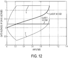
- the dynamic gate bias and RF drive voltages "V,” according to an exemplary embodiment, are shown in Figure 12 and these voltages correspond to a termination resistance R term twice the load resistance.
- the corresponding voltages for a conventional class F amplifier are also shown in Figure 12 for reference.
- the upper line corresponds to the RF drive voltage and the lower line corresponds to the gate bias voltage.
- the gate bias can be dynamic (variable), contrary to the conventional amplifiers for which the gate bias is constant, i.e., fixed.
- the (drain) efficiency "E" versus the output amplitude of one exemplary embodiment is shown in Figure 13 , together with the efficiency of the conventional class F amplifier.
- Figure 13 shows that the efficiency at low and medium amplitudes is higher for the exemplary embodiment than for the class F amplifier. For the highest amplitudes, the efficiency of the exemplary embodiment is lower than for the conventional class F amplifier.
- most of the signal amplitude distributions encountered in multicarrier and multi-user radio transmitters have the highest density at medium amplitudes, for which the amplifier of the exemplary embodiment is superior to the conventional amplifier, and thus, a better choice.
- a high RF drive voltage might be a disadvantage if the gain of the transistor is low, in which case the drain efficiency of the transistor may be traded against a low drive signal power.
- This drawback may be reduced by driving the gate directly with a PWM-like waveform.
- the gate of the transistor is driven with the PWM-like waveform.
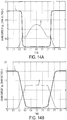
- an output power may be higher than for a conventional class F amplifier.
- the higher output power is achieved by the exemplary embodiment because the conventional class F amplifier has a peaky current waveform at the highest output amplitudes, whereas the exemplary embodiment has a flatter shaped current waveform.
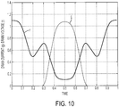
- This shape of the current waveform is shown in Figures 14A and B.
- Figure 14B shows the current waveform (g) of the conventional class F amplifier at its peak output power while
- Figure 14B shows the current waveform (g) of an exemplary embodiment in which R Term is substantially equal to R Load , at its peak output power.
- the flatter current pulse of the exemplary embodiment contains more energy at the fundamental frequency. This flatter shape of the peak current more than compensates for the less square voltage waveform, and thus the power output of the amplifier according to this exemplary embodiment is higher than the power output of the conventional class F amplifier.
- the maximum output power of an amplifier (C/F) is compared with conventional class AB and class F amplifiers, as shown in Figure 15 .
- the peak RF drive voltages, peak drain voltages, and peak drain currents were designed (by properly setting the supply voltage and load resistance) to be the same for all four amplifiers.
- the same transistor was used for all four amplifiers.
- the class F amplifier is complemented in this example with a dynamic gate bias (DGB), which results in an increased output power above its point of maximum efficiency due to the increased gate bias voltage.
- DGB dynamic gate bias
- Figure 15 shows the efficiency curves for the above discussed amplifiers having the maximum output potential.
- a conventional class AB amplifier with 2 dB compression at maximum output was chosen as a reference.
- Another conventional class AB amplifier, with almost no compression, is shown as reference of the maximum output for a non-DGB, non-class F amplifier.
- the novel amplifier behaves like a hybrid amplifier, i.e., an amplifier having features from both class F and class C.
- the class F amplifier is seen to have 1.1 dB higher output power than the reference class AB system ("no compression"), and the amplifier of the exemplary embodiment has a further 0.6 dB higher output power than the class F amplifier.
- an inverse class C/F amplifier is considered.
- the even harmonics are terminated in an impedance that is close in size to the load. According to an exemplary embodiment, a method for operating one of the above discussed power amplifiers is presented next.
- the method includes a step 160 of generating impedances at harmonic frequencies such that the power amplifier operates in a class C mode in a low output amplitude range and in a class F or inverse class F mode in a high output amplitude range.
- the harmonics in this step may be odd or even harmonics.
- Dynamic gate bias (DGB), Pulse Width Modulation (PWM), or some other method that determines a variable RF current pulsewidth, may be used with the novel amplifier. Controlling one or more overtones in the input signal in one exemplary embodiment, may be beneficial in the dynamic gate bias case.
- the exemplary amplifiers discussed above may be applied to Doherty, Chireix, Load Modulation (LM), Dynamic Drain Bias (DDB), and Envelope Elimination and Restoration (EER) amplifiers.
- the harmonic termination impedance preferably lies in the upper size range, because these amplifiers have a relatively large portion of their operation with a high voltage swing relative to the supply voltage.
- Doherty, Chireix, or LM amplifier there may be a trade off between the efficiency in the upper region of the high voltage swing operation and the efficiency at amplitudes below this region.
- one or more of the exemplary amplifiers discussed above have a higher output power than a conventional class F amplifier, for equal transistors and equal limitations, under both PWM drive and most DGB + sinusoidal RF drive conditions.
- the exemplary amplifiers are more robust than the conventional class F amplifiers because the relatively low impedance termination of harmonics reduces the inadvertent transient voltages, and narrow current pulses due to fast changes in the signal, start up processes, etc.
- the exemplary amplifiers are also more broadband than a conventional class F amplifier, since the Q values of the harmonic resonators are lower.
- Another advantage of one or more exemplary embodiments is that a higher average efficiency may be obtained.
- the higher efficiency may be obtained in single transistor amplifiers, Doherty, Chireix, LM, DDB, and EER systems as well as most other composite amplifiers.
- the exemplary amplifiers have a higher average efficiency, are more robust, are more broadband, and have a higher output power than conventional amplifiers.
- the disclosed exemplary embodiments provide a device, a system, and a method for amplifying a signal. It should be understood that this description is not intended to limit the invention. On the contrary, the exemplary embodiments are intended to cover alternatives, modifications and equivalents, which are included in the spirit and scope of the invention as defined by the appended claims. Further, in the detailed description of the exemplary embodiments, numerous specific details are set forth in order to provide a comprehensive understanding of the claimed invention. However, one skilled in the art would understand that various embodiments may be practiced without such specific details.
- the exemplary embodiments may be embodied in a base station of a telecommunication network, a mobile terminal as a phone, PDA, or any communication device capable of amplifying signals.
Landscapes
- Engineering & Computer Science (AREA)
- Power Engineering (AREA)
- Amplifiers (AREA)
Claims (9)
- Leistungsverstärker (10), der zum Verstärken eines Hochfrequenzsignals konfiguriert ist und eine Ausgangsschaltung (18) umfasst, die Impedanzen bei harmonischen Frequenzen erzeugt, sodass der Leistungsverstärker (10) in einem Klasse-C-Modus in einem niedrigen Ausgangsamplitudenbereich und in einem Klasse-F- oder inversen Klasse-F-Modus in einem hohen Ausgangsamplitudenbereich arbeitet,
wobei der Leistungsverstärker (10) Folgendes umfasst:einen Transistor (12), der zum Erzeugen eines Ausgangshochfrequenzsignals konfiguriert ist; unddie Ausgangsschaltung (18), die mit dem Transistor (12) verbunden und zum Empfangen des Hochfrequenzausgangssignals konfiguriert ist und Impedanzen einschließt;wobei der Ausgangsschaltung (18) Folgendes umfasst:einen Parallelresonator (20), der zum Blockieren einer Grundfrequenz konfiguriert und zwischen einem Emitter und einem Kollektor des Transistors (12) geschaltet ist, wobei der Parallelresonator (20) mit einem Widerstand (30) in Reihe geschaltet ist, und wobei ein Wert des Widerstands (30) innerhalb von 10 % eines Widerstands einer Last (28) liegt, wobei die Last (28) einen Widerstand (Rload) umfasst und in Reihe mit einem seriellen Resonator (26) geschaltet ist, der zwischen dem Emitter des Transistors (12) und der Last (28) geschaltet ist, und wobei der Widerstand (Rload) parallel mit dem Parallelresonator (20) und dem Widerstand (30) bei einer maximalen Ausgangsleistung geschaltet ist; undeinen ersten seriellen Resonator (22), der zum Resonieren mit der doppelten Grundfrequenz konfiguriert ist, der parallel zu einem Kondensator (46) zwischen dem Emitter und dem Kollektor des Transistors (12) geschaltet ist. - Leistungsverstärker (10) nach Anspruch 1, wobei die harmonischen Frequenzen ungerade harmonische Frequenzen sind.
- Leistungsverstärker (10) nach Anspruch 1, wobei die harmonischen Frequenzen geradzahlige harmonische Frequenzen sind.
- Leistungsverstärker (10) nach Anspruch 1, wobei der Klasse-C-Modus durch das Aufweisen von schmalen Ausgangsstromimpulsen an dem Transistor (12) des Leistungsverstärkers (10) definiert ist.
- Leistungsverstärker (10) nach Anspruch 1, wobei der Klasse-F-Modus durch eine quadratische Ausgangsspannungswellenform an dem Transistor (12) des Leistungsverstärkers (10) definiert ist.
- Leistungsverstärker (10) nach Anspruch 1, wobei der Umkehrklasse-F-Modus durch eine quadratische Ausgangsstromwellenform an dem Transistor (12) des Leistungsverstärkers (10) definiert ist.
- Leistungsverstärker (10) nach Anspruch 1, wobei die Impedanzen eine endliche Impedanz bei einer oder mehreren Harmonien der Grundfrequenz einschließen und die endliche Impedanz einen Spannungshub an den Harmonien reduziert.
- Leistungsverstärker (10) nach Anspruch 1, wobei eine Gate-Spannung des Transistors (12) eine dynamische Gate-Vorspannung umfasst.
- Leistungsverstärker (10) nach Anspruch 1, wobei eine Gate-Spannung des Transistors (12) eine pulsweitenmodulierte Wellenform ist.
Applications Claiming Priority (1)
| Application Number | Priority Date | Filing Date | Title |
|---|---|---|---|
| PCT/SE2008/050979 WO2010024746A1 (en) | 2008-09-01 | 2008-09-01 | Hybrid class amplifier |
Publications (3)
| Publication Number | Publication Date |
|---|---|
| EP2321901A1 EP2321901A1 (de) | 2011-05-18 |
| EP2321901A4 EP2321901A4 (de) | 2016-11-30 |
| EP2321901B1 true EP2321901B1 (de) | 2019-08-07 |
Family
ID=41721716
Family Applications (1)
| Application Number | Title | Priority Date | Filing Date |
|---|---|---|---|
| EP08813476.2A Active EP2321901B1 (de) | 2008-09-01 | 2008-09-01 | Hybrid-klasse-verstärker |
Country Status (4)
| Country | Link |
|---|---|
| US (2) | US8350627B2 (de) |
| EP (1) | EP2321901B1 (de) |
| CN (1) | CN102138281B (de) |
| WO (1) | WO2010024746A1 (de) |
Families Citing this family (26)
| Publication number | Priority date | Publication date | Assignee | Title |
|---|---|---|---|---|
| US8441321B2 (en) | 2008-12-09 | 2013-05-14 | Telefonaktiebolaget L M Ericsson (Publ) | Multi-stage amplifier |
| EP2584698A4 (de) * | 2010-06-21 | 2013-10-16 | Panasonic Corp | Hochfrequenz-verstärkerschaltung |
| WO2012000129A1 (en) * | 2010-06-29 | 2012-01-05 | Telefonaktiebolaget L M Ericsson (Publ) | Multi-band power amplifier |
| WO2013001711A1 (ja) * | 2011-06-28 | 2013-01-03 | パナソニック株式会社 | 高周波電力増幅器 |
| WO2013066466A2 (en) * | 2011-08-12 | 2013-05-10 | Bae Systems Integration And Electronic Systems Integration Inc. | Low voltage high efficiency gallium arsenide power amplifier |
| WO2013031865A1 (ja) * | 2011-08-29 | 2013-03-07 | 国立大学法人 電気通信大学 | 高効率電力増幅器 |
| US9679869B2 (en) | 2011-09-02 | 2017-06-13 | Skyworks Solutions, Inc. | Transmission line for high performance radio frequency applications |
| JP5571047B2 (ja) * | 2011-09-15 | 2014-08-13 | 株式会社東芝 | 電力増幅装置 |
| KR102250612B1 (ko) | 2012-06-14 | 2021-05-10 | 스카이워크스 솔루션즈, 인코포레이티드 | 고조파 종단 회로를 포함하는 전력 증폭기 모듈 및 관련된 시스템, 장치, 및 방법 |
| US9294056B2 (en) | 2013-03-12 | 2016-03-22 | Peregrine Semiconductor Corporation | Scalable periphery tunable matching power amplifier |
| US9602063B2 (en) | 2013-03-12 | 2017-03-21 | Peregrine Semiconductor Corporation | Variable impedance match and variable harmonic terminations for different modes and frequency bands |
| US9024691B2 (en) * | 2013-05-17 | 2015-05-05 | Georgia Tech Research Corporation | Adaptive power amplifier and methods of making same |
| EP2933646B1 (de) * | 2014-04-17 | 2019-04-17 | Siemens Aktiengesellschaft | Präzisionsmessung von Spannungsabfall über ein Halbleiterschaltelement |
| US9503025B2 (en) * | 2014-07-11 | 2016-11-22 | Skyworks Solutions, Inc. | Power amplifier with termination circuit and resonant circuit |
| US9319010B1 (en) | 2014-12-16 | 2016-04-19 | Freescale Semiconductor Inc. | Inverse class F amplifiers with intrinsic capacitance compensation |
| CN105141262B (zh) * | 2015-07-21 | 2018-06-05 | 苏州能讯高能半导体有限公司 | 一种适用于f类或逆f类功率放大器的放大模块 |
| JP6581477B2 (ja) * | 2015-11-17 | 2019-09-25 | 株式会社東芝 | 増幅器 |
| US9929704B2 (en) * | 2015-12-14 | 2018-03-27 | Qualcomm Incorporated | Class E2 amplifier |
| US9673766B1 (en) * | 2016-05-18 | 2017-06-06 | Nxp Usa, Inc. | Class F amplifiers using resonant circuits in an output matching network |
| US10193509B1 (en) | 2017-07-28 | 2019-01-29 | Avago Technologies International Sales Pte. Limited | Power amplifier harmonic matching network |
| US10381988B2 (en) * | 2017-09-15 | 2019-08-13 | Qualcomm Incorporated | Methods and apparatuses for ruggedizing a power amplifier against breakdown using harmonic tuning |
| US10637405B2 (en) * | 2018-08-14 | 2020-04-28 | Nxp Usa, Inc. | Wideband biasing of high power amplifiers |
| EP3754780B1 (de) | 2019-06-17 | 2022-07-27 | Carrier Corporation | Mikrostreifen-dc-block |
| CN110311640B (zh) * | 2019-06-27 | 2024-04-09 | 杭州电子科技大学 | 宽带混合f/j类功率放大器及其设计方法 |
| JP2023013446A (ja) * | 2021-07-16 | 2023-01-26 | 株式会社村田製作所 | 電力増幅回路 |
| US12562690B2 (en) * | 2021-11-01 | 2026-02-24 | Qualcomm Incorporated | Linearization of low gain low-noise amplifiers through third-order distortion cancellation |
Family Cites Families (4)
| Publication number | Priority date | Publication date | Assignee | Title |
|---|---|---|---|---|
| JPH0732335B2 (ja) * | 1990-11-16 | 1995-04-10 | 日本電信電話株式会社 | 高周波増幅器 |
| JP2005080114A (ja) | 2003-09-02 | 2005-03-24 | Kenwood Corp | オーディオ信号増幅機能付き装置及びオーディオ放送受信機用増幅器制御方法 |
| JP4659826B2 (ja) * | 2004-06-23 | 2011-03-30 | ペレグリン セミコンダクター コーポレーション | Rfフロントエンド集積回路 |
| FR2911447B1 (fr) * | 2007-01-16 | 2011-12-16 | St Microelectronics Sa | Amplificateur de puissance reconfigurable et utilisation d'un tel amplificateur pour la realisation d'un etage d'amplification multistandard pour la telephonie mobile |
-
2008
- 2008-09-01 EP EP08813476.2A patent/EP2321901B1/de active Active
- 2008-09-01 CN CN200880130947.7A patent/CN102138281B/zh not_active Expired - Fee Related
- 2008-09-01 US US13/061,453 patent/US8350627B2/en not_active Expired - Fee Related
- 2008-09-01 WO PCT/SE2008/050979 patent/WO2010024746A1/en not_active Ceased
-
2012
- 2012-12-12 US US13/712,513 patent/US8593225B2/en active Active
Non-Patent Citations (1)
| Title |
|---|
| None * |
Also Published As
| Publication number | Publication date |
|---|---|
| US8593225B2 (en) | 2013-11-26 |
| US20130106520A1 (en) | 2013-05-02 |
| US8350627B2 (en) | 2013-01-08 |
| US20110163814A1 (en) | 2011-07-07 |
| CN102138281A (zh) | 2011-07-27 |
| WO2010024746A1 (en) | 2010-03-04 |
| EP2321901A4 (de) | 2016-11-30 |
| CN102138281B (zh) | 2015-07-08 |
| EP2321901A1 (de) | 2011-05-18 |
Similar Documents
| Publication | Publication Date | Title |
|---|---|---|
| EP2321901B1 (de) | Hybrid-klasse-verstärker | |
| US10763798B2 (en) | Variable impedance match and variable harmonic terminations for different modes and frequency bands | |
| JP6680235B2 (ja) | 電力増幅回路および高周波モジュール | |
| US9806673B2 (en) | Class-E outphasing power amplifier with efficiency and output power enhancement circuits and method | |
| US8269555B2 (en) | Efficient linear LINC power amplifier | |
| Kang et al. | Design of bandwidth-enhanced Doherty power amplifiers for handset applications | |
| CN1391359A (zh) | 非对称偏压的高线性平衡放大器 | |
| US20170373645A1 (en) | Doherty-Chireix Combined Amplifier | |
| EP2374210B1 (de) | Mehrstufiger verstärker | |
| CN1400742A (zh) | 微波功率放大器 | |
| CN1391358A (zh) | 将多赫尔蒂用作线性化微波放大器的预失真电路 | |
| US20230020495A1 (en) | Load-modulated push-pull power amplifier | |
| Kang et al. | Design of Doherty power amplifiers for handset applications | |
| JP5095755B2 (ja) | 再構成可能なパワーアンプおよび移動電話通信の多標準増幅段での使用 | |
| CN1182747C (zh) | 有效生成低功率射频信号的电路 | |
| US8174311B2 (en) | Switching amplifier | |
| CN102498662B (zh) | 移动通信系统中的方法和设备 | |
| US8653886B2 (en) | Method and arrangement in a mobile communications system | |
| EP2705601B1 (de) | Breitband-und rekonfigurierbarer doherty-basierter verstärker | |
| CN104953965B (zh) | 混合类放大器 | |
| Mimis et al. | A reactively load-modulated RF low-power amplifier with multilevel supply voltage for multi-standard RF front-ends | |
| Reynaert et al. | CMOS RF PA design: using complexity to solve the linearity and efficiency trade-off | |
| Lee et al. | A 5.8-GHz power amplifier with an on-chip tunable output matching network | |
| Parmar et al. | BER, MER Analysis of High Power Amplifier designed with LDMOS | |
| Nemati et al. | Practical realizations of high efficiency switched mode power amplifiers |
Legal Events
| Date | Code | Title | Description |
|---|---|---|---|
| PUAI | Public reference made under article 153(3) epc to a published international application that has entered the european phase |
Free format text: ORIGINAL CODE: 0009012 |
|
| AK | Designated contracting states |
Kind code of ref document: A1 Designated state(s): AT BE BG CH CY CZ DE DK EE ES FI FR GB GR HR HU IE IS IT LI LT LU LV MC MT NL NO PL PT RO SE SI SK TR |
|
| AX | Request for extension of the european patent |
Extension state: AL BA MK RS |
|
| 17P | Request for examination filed |
Effective date: 20110210 |
|
| DAX | Request for extension of the european patent (deleted) | ||
| RA4 | Supplementary search report drawn up and despatched (corrected) |
Effective date: 20161028 |
|
| RIC1 | Information provided on ipc code assigned before grant |
Ipc: H03F 1/56 20060101ALI20161024BHEP Ipc: H03F 3/19 20060101ALI20161024BHEP Ipc: H03F 1/02 20060101ALI20161024BHEP Ipc: H03F 3/217 20060101AFI20161024BHEP |
|
| STAA | Information on the status of an ep patent application or granted ep patent |
Free format text: STATUS: EXAMINATION IS IN PROGRESS |
|
| 17Q | First examination report despatched |
Effective date: 20170526 |
|
| REG | Reference to a national code |
Ref country code: DE Ref legal event code: R079 Ref document number: 602008060858 Country of ref document: DE Free format text: PREVIOUS MAIN CLASS: H03F0003217000 Ipc: H03F0003160000 |
|
| GRAP | Despatch of communication of intention to grant a patent |
Free format text: ORIGINAL CODE: EPIDOSNIGR1 |
|
| STAA | Information on the status of an ep patent application or granted ep patent |
Free format text: STATUS: GRANT OF PATENT IS INTENDED |
|
| RIC1 | Information provided on ipc code assigned before grant |
Ipc: H03F 3/16 20060101AFI20190522BHEP Ipc: H03F 1/56 20060101ALI20190522BHEP Ipc: H03F 3/19 20060101ALI20190522BHEP Ipc: H03F 3/217 20060101ALI20190522BHEP Ipc: H03F 1/02 20060101ALI20190522BHEP |
|
| GRAS | Grant fee paid |
Free format text: ORIGINAL CODE: EPIDOSNIGR3 |
|
| INTG | Intention to grant announced |
Effective date: 20190607 |
|
| GRAA | (expected) grant |
Free format text: ORIGINAL CODE: 0009210 |
|
| STAA | Information on the status of an ep patent application or granted ep patent |
Free format text: STATUS: THE PATENT HAS BEEN GRANTED |
|
| AK | Designated contracting states |
Kind code of ref document: B1 Designated state(s): AT BE BG CH CY CZ DE DK EE ES FI FR GB GR HR HU IE IS IT LI LT LU LV MC MT NL NO PL PT RO SE SI SK TR |
|
| REG | Reference to a national code |
Ref country code: GB Ref legal event code: FG4D |
|
| REG | Reference to a national code |
Ref country code: CH Ref legal event code: EP Ref country code: AT Ref legal event code: REF Ref document number: 1165369 Country of ref document: AT Kind code of ref document: T Effective date: 20190815 |
|
| REG | Reference to a national code |
Ref country code: DE Ref legal event code: R096 Ref document number: 602008060858 Country of ref document: DE |
|
| REG | Reference to a national code |
Ref country code: IE Ref legal event code: FG4D |
|
| REG | Reference to a national code |
Ref country code: NL Ref legal event code: MP Effective date: 20190807 |
|
| REG | Reference to a national code |
Ref country code: LT Ref legal event code: MG4D |
|
| PG25 | Lapsed in a contracting state [announced via postgrant information from national office to epo] |
Ref country code: FI Free format text: LAPSE BECAUSE OF FAILURE TO SUBMIT A TRANSLATION OF THE DESCRIPTION OR TO PAY THE FEE WITHIN THE PRESCRIBED TIME-LIMIT Effective date: 20190807 Ref country code: BG Free format text: LAPSE BECAUSE OF FAILURE TO SUBMIT A TRANSLATION OF THE DESCRIPTION OR TO PAY THE FEE WITHIN THE PRESCRIBED TIME-LIMIT Effective date: 20191107 Ref country code: SE Free format text: LAPSE BECAUSE OF FAILURE TO SUBMIT A TRANSLATION OF THE DESCRIPTION OR TO PAY THE FEE WITHIN THE PRESCRIBED TIME-LIMIT Effective date: 20190807 Ref country code: HR Free format text: LAPSE BECAUSE OF FAILURE TO SUBMIT A TRANSLATION OF THE DESCRIPTION OR TO PAY THE FEE WITHIN THE PRESCRIBED TIME-LIMIT Effective date: 20190807 Ref country code: NO Free format text: LAPSE BECAUSE OF FAILURE TO SUBMIT A TRANSLATION OF THE DESCRIPTION OR TO PAY THE FEE WITHIN THE PRESCRIBED TIME-LIMIT Effective date: 20191107 Ref country code: PT Free format text: LAPSE BECAUSE OF FAILURE TO SUBMIT A TRANSLATION OF THE DESCRIPTION OR TO PAY THE FEE WITHIN THE PRESCRIBED TIME-LIMIT Effective date: 20191209 Ref country code: LT Free format text: LAPSE BECAUSE OF FAILURE TO SUBMIT A TRANSLATION OF THE DESCRIPTION OR TO PAY THE FEE WITHIN THE PRESCRIBED TIME-LIMIT Effective date: 20190807 Ref country code: NL Free format text: LAPSE BECAUSE OF FAILURE TO SUBMIT A TRANSLATION OF THE DESCRIPTION OR TO PAY THE FEE WITHIN THE PRESCRIBED TIME-LIMIT Effective date: 20190807 |
|
| REG | Reference to a national code |
Ref country code: AT Ref legal event code: MK05 Ref document number: 1165369 Country of ref document: AT Kind code of ref document: T Effective date: 20190807 |
|
| PG25 | Lapsed in a contracting state [announced via postgrant information from national office to epo] |
Ref country code: LV Free format text: LAPSE BECAUSE OF FAILURE TO SUBMIT A TRANSLATION OF THE DESCRIPTION OR TO PAY THE FEE WITHIN THE PRESCRIBED TIME-LIMIT Effective date: 20190807 Ref country code: GR Free format text: LAPSE BECAUSE OF FAILURE TO SUBMIT A TRANSLATION OF THE DESCRIPTION OR TO PAY THE FEE WITHIN THE PRESCRIBED TIME-LIMIT Effective date: 20191108 Ref country code: ES Free format text: LAPSE BECAUSE OF FAILURE TO SUBMIT A TRANSLATION OF THE DESCRIPTION OR TO PAY THE FEE WITHIN THE PRESCRIBED TIME-LIMIT Effective date: 20190807 Ref country code: IS Free format text: LAPSE BECAUSE OF FAILURE TO SUBMIT A TRANSLATION OF THE DESCRIPTION OR TO PAY THE FEE WITHIN THE PRESCRIBED TIME-LIMIT Effective date: 20191207 |
|
| PG25 | Lapsed in a contracting state [announced via postgrant information from national office to epo] |
Ref country code: TR Free format text: LAPSE BECAUSE OF FAILURE TO SUBMIT A TRANSLATION OF THE DESCRIPTION OR TO PAY THE FEE WITHIN THE PRESCRIBED TIME-LIMIT Effective date: 20190807 |
|
| PG25 | Lapsed in a contracting state [announced via postgrant information from national office to epo] |
Ref country code: RO Free format text: LAPSE BECAUSE OF FAILURE TO SUBMIT A TRANSLATION OF THE DESCRIPTION OR TO PAY THE FEE WITHIN THE PRESCRIBED TIME-LIMIT Effective date: 20190807 Ref country code: PL Free format text: LAPSE BECAUSE OF FAILURE TO SUBMIT A TRANSLATION OF THE DESCRIPTION OR TO PAY THE FEE WITHIN THE PRESCRIBED TIME-LIMIT Effective date: 20190807 Ref country code: AT Free format text: LAPSE BECAUSE OF FAILURE TO SUBMIT A TRANSLATION OF THE DESCRIPTION OR TO PAY THE FEE WITHIN THE PRESCRIBED TIME-LIMIT Effective date: 20190807 Ref country code: EE Free format text: LAPSE BECAUSE OF FAILURE TO SUBMIT A TRANSLATION OF THE DESCRIPTION OR TO PAY THE FEE WITHIN THE PRESCRIBED TIME-LIMIT Effective date: 20190807 Ref country code: IT Free format text: LAPSE BECAUSE OF FAILURE TO SUBMIT A TRANSLATION OF THE DESCRIPTION OR TO PAY THE FEE WITHIN THE PRESCRIBED TIME-LIMIT Effective date: 20190807 Ref country code: DK Free format text: LAPSE BECAUSE OF FAILURE TO SUBMIT A TRANSLATION OF THE DESCRIPTION OR TO PAY THE FEE WITHIN THE PRESCRIBED TIME-LIMIT Effective date: 20190807 |
|
| PG25 | Lapsed in a contracting state [announced via postgrant information from national office to epo] |
Ref country code: SK Free format text: LAPSE BECAUSE OF FAILURE TO SUBMIT A TRANSLATION OF THE DESCRIPTION OR TO PAY THE FEE WITHIN THE PRESCRIBED TIME-LIMIT Effective date: 20190807 Ref country code: CZ Free format text: LAPSE BECAUSE OF FAILURE TO SUBMIT A TRANSLATION OF THE DESCRIPTION OR TO PAY THE FEE WITHIN THE PRESCRIBED TIME-LIMIT Effective date: 20190807 Ref country code: IS Free format text: LAPSE BECAUSE OF FAILURE TO SUBMIT A TRANSLATION OF THE DESCRIPTION OR TO PAY THE FEE WITHIN THE PRESCRIBED TIME-LIMIT Effective date: 20200224 Ref country code: MC Free format text: LAPSE BECAUSE OF FAILURE TO SUBMIT A TRANSLATION OF THE DESCRIPTION OR TO PAY THE FEE WITHIN THE PRESCRIBED TIME-LIMIT Effective date: 20190807 |
|
| REG | Reference to a national code |
Ref country code: CH Ref legal event code: PL |
|
| REG | Reference to a national code |
Ref country code: DE Ref legal event code: R097 Ref document number: 602008060858 Country of ref document: DE |
|
| PLBE | No opposition filed within time limit |
Free format text: ORIGINAL CODE: 0009261 |
|
| STAA | Information on the status of an ep patent application or granted ep patent |
Free format text: STATUS: NO OPPOSITION FILED WITHIN TIME LIMIT |
|
| PG2D | Information on lapse in contracting state deleted |
Ref country code: IS |
|
| PG25 | Lapsed in a contracting state [announced via postgrant information from national office to epo] |
Ref country code: CH Free format text: LAPSE BECAUSE OF NON-PAYMENT OF DUE FEES Effective date: 20190930 Ref country code: LI Free format text: LAPSE BECAUSE OF NON-PAYMENT OF DUE FEES Effective date: 20190930 Ref country code: LU Free format text: LAPSE BECAUSE OF NON-PAYMENT OF DUE FEES Effective date: 20190901 Ref country code: IE Free format text: LAPSE BECAUSE OF NON-PAYMENT OF DUE FEES Effective date: 20190901 |
|
| REG | Reference to a national code |
Ref country code: BE Ref legal event code: MM Effective date: 20190930 |
|
| 26N | No opposition filed |
Effective date: 20200603 |
|
| PG25 | Lapsed in a contracting state [announced via postgrant information from national office to epo] |
Ref country code: BE Free format text: LAPSE BECAUSE OF NON-PAYMENT OF DUE FEES Effective date: 20190930 Ref country code: SI Free format text: LAPSE BECAUSE OF FAILURE TO SUBMIT A TRANSLATION OF THE DESCRIPTION OR TO PAY THE FEE WITHIN THE PRESCRIBED TIME-LIMIT Effective date: 20190807 |
|
| PGFP | Annual fee paid to national office [announced via postgrant information from national office to epo] |
Ref country code: FR Payment date: 20200925 Year of fee payment: 13 |
|
| PG25 | Lapsed in a contracting state [announced via postgrant information from national office to epo] |
Ref country code: CY Free format text: LAPSE BECAUSE OF FAILURE TO SUBMIT A TRANSLATION OF THE DESCRIPTION OR TO PAY THE FEE WITHIN THE PRESCRIBED TIME-LIMIT Effective date: 20190807 |
|
| PG25 | Lapsed in a contracting state [announced via postgrant information from national office to epo] |
Ref country code: HU Free format text: LAPSE BECAUSE OF FAILURE TO SUBMIT A TRANSLATION OF THE DESCRIPTION OR TO PAY THE FEE WITHIN THE PRESCRIBED TIME-LIMIT; INVALID AB INITIO Effective date: 20080901 Ref country code: MT Free format text: LAPSE BECAUSE OF FAILURE TO SUBMIT A TRANSLATION OF THE DESCRIPTION OR TO PAY THE FEE WITHIN THE PRESCRIBED TIME-LIMIT Effective date: 20190807 |
|
| PG25 | Lapsed in a contracting state [announced via postgrant information from national office to epo] |
Ref country code: FR Free format text: LAPSE BECAUSE OF NON-PAYMENT OF DUE FEES Effective date: 20210930 |
|
| PGFP | Annual fee paid to national office [announced via postgrant information from national office to epo] |
Ref country code: GB Payment date: 20220927 Year of fee payment: 15 |
|
| GBPC | Gb: european patent ceased through non-payment of renewal fee |
Effective date: 20230901 |
|
| PG25 | Lapsed in a contracting state [announced via postgrant information from national office to epo] |
Ref country code: GB Free format text: LAPSE BECAUSE OF NON-PAYMENT OF DUE FEES Effective date: 20230901 |
|
| PG25 | Lapsed in a contracting state [announced via postgrant information from national office to epo] |
Ref country code: GB Free format text: LAPSE BECAUSE OF NON-PAYMENT OF DUE FEES Effective date: 20230901 |
|
| PGFP | Annual fee paid to national office [announced via postgrant information from national office to epo] |
Ref country code: DE Payment date: 20250929 Year of fee payment: 18 |