EP2323191A2 - Composant photoélectrique organique - Google Patents
Composant photoélectrique organique Download PDFInfo
- Publication number
- EP2323191A2 EP2323191A2 EP20100191333 EP10191333A EP2323191A2 EP 2323191 A2 EP2323191 A2 EP 2323191A2 EP 20100191333 EP20100191333 EP 20100191333 EP 10191333 A EP10191333 A EP 10191333A EP 2323191 A2 EP2323191 A2 EP 2323191A2
- Authority
- EP
- European Patent Office
- Prior art keywords
- electrode
- substrate
- photoelectric device
- organic photoelectric
- cover
- Prior art date
- Legal status (The legal status is an assumption and is not a legal conclusion. Google has not performed a legal analysis and makes no representation as to the accuracy of the status listed.)
- Withdrawn
Links
Images


Classifications
-
- H—ELECTRICITY
- H10—SEMICONDUCTOR DEVICES; ELECTRIC SOLID-STATE DEVICES NOT OTHERWISE PROVIDED FOR
- H10K—ORGANIC ELECTRIC SOLID-STATE DEVICES
- H10K39/00—Integrated devices, or assemblies of multiple devices, comprising at least one organic radiation-sensitive element covered by group H10K30/00
- H10K39/10—Organic photovoltaic [PV] modules; Arrays of single organic PV cells
-
- H—ELECTRICITY
- H10—SEMICONDUCTOR DEVICES; ELECTRIC SOLID-STATE DEVICES NOT OTHERWISE PROVIDED FOR
- H10K—ORGANIC ELECTRIC SOLID-STATE DEVICES
- H10K30/00—Organic devices sensitive to infrared radiation, light, electromagnetic radiation of shorter wavelength or corpuscular radiation
- H10K30/80—Constructional details
- H10K30/88—Passivation; Containers; Encapsulations
-
- H—ELECTRICITY
- H10—SEMICONDUCTOR DEVICES; ELECTRIC SOLID-STATE DEVICES NOT OTHERWISE PROVIDED FOR
- H10K—ORGANIC ELECTRIC SOLID-STATE DEVICES
- H10K50/00—Organic light-emitting devices
- H10K50/80—Constructional details
- H10K50/805—Electrodes
-
- H—ELECTRICITY
- H10—SEMICONDUCTOR DEVICES; ELECTRIC SOLID-STATE DEVICES NOT OTHERWISE PROVIDED FOR
- H10K—ORGANIC ELECTRIC SOLID-STATE DEVICES
- H10K50/00—Organic light-emitting devices
- H10K50/80—Constructional details
- H10K50/84—Passivation; Containers; Encapsulations
- H10K50/841—Self-supporting sealing arrangements
-
- H—ELECTRICITY
- H10—SEMICONDUCTOR DEVICES; ELECTRIC SOLID-STATE DEVICES NOT OTHERWISE PROVIDED FOR
- H10K—ORGANIC ELECTRIC SOLID-STATE DEVICES
- H10K50/00—Organic light-emitting devices
- H10K50/80—Constructional details
- H10K50/84—Passivation; Containers; Encapsulations
- H10K50/842—Containers
- H10K50/8423—Metallic sealing arrangements
-
- H—ELECTRICITY
- H10—SEMICONDUCTOR DEVICES; ELECTRIC SOLID-STATE DEVICES NOT OTHERWISE PROVIDED FOR
- H10K—ORGANIC ELECTRIC SOLID-STATE DEVICES
- H10K50/00—Organic light-emitting devices
- H10K50/80—Constructional details
- H10K50/84—Passivation; Containers; Encapsulations
- H10K50/842—Containers
- H10K50/8426—Peripheral sealing arrangements, e.g. adhesives, sealants
-
- H—ELECTRICITY
- H10—SEMICONDUCTOR DEVICES; ELECTRIC SOLID-STATE DEVICES NOT OTHERWISE PROVIDED FOR
- H10K—ORGANIC ELECTRIC SOLID-STATE DEVICES
- H10K50/00—Organic light-emitting devices
- H10K50/80—Constructional details
- H10K50/84—Passivation; Containers; Encapsulations
- H10K50/842—Containers
- H10K50/8428—Vertical spacers, e.g. arranged between the sealing arrangement and the OLED
-
- Y—GENERAL TAGGING OF NEW TECHNOLOGICAL DEVELOPMENTS; GENERAL TAGGING OF CROSS-SECTIONAL TECHNOLOGIES SPANNING OVER SEVERAL SECTIONS OF THE IPC; TECHNICAL SUBJECTS COVERED BY FORMER USPC CROSS-REFERENCE ART COLLECTIONS [XRACs] AND DIGESTS
- Y02—TECHNOLOGIES OR APPLICATIONS FOR MITIGATION OR ADAPTATION AGAINST CLIMATE CHANGE
- Y02B—CLIMATE CHANGE MITIGATION TECHNOLOGIES RELATED TO BUILDINGS, e.g. HOUSING, HOUSE APPLIANCES OR RELATED END-USER APPLICATIONS
- Y02B10/00—Integration of renewable energy sources in buildings
- Y02B10/10—Photovoltaic [PV]
-
- Y—GENERAL TAGGING OF NEW TECHNOLOGICAL DEVELOPMENTS; GENERAL TAGGING OF CROSS-SECTIONAL TECHNOLOGIES SPANNING OVER SEVERAL SECTIONS OF THE IPC; TECHNICAL SUBJECTS COVERED BY FORMER USPC CROSS-REFERENCE ART COLLECTIONS [XRACs] AND DIGESTS
- Y02—TECHNOLOGIES OR APPLICATIONS FOR MITIGATION OR ADAPTATION AGAINST CLIMATE CHANGE
- Y02E—REDUCTION OF GREENHOUSE GAS [GHG] EMISSIONS, RELATED TO ENERGY GENERATION, TRANSMISSION OR DISTRIBUTION
- Y02E10/00—Energy generation through renewable energy sources
- Y02E10/50—Photovoltaic [PV] energy
- Y02E10/549—Organic PV cells
-
- Y—GENERAL TAGGING OF NEW TECHNOLOGICAL DEVELOPMENTS; GENERAL TAGGING OF CROSS-SECTIONAL TECHNOLOGIES SPANNING OVER SEVERAL SECTIONS OF THE IPC; TECHNICAL SUBJECTS COVERED BY FORMER USPC CROSS-REFERENCE ART COLLECTIONS [XRACs] AND DIGESTS
- Y02—TECHNOLOGIES OR APPLICATIONS FOR MITIGATION OR ADAPTATION AGAINST CLIMATE CHANGE
- Y02P—CLIMATE CHANGE MITIGATION TECHNOLOGIES IN THE PRODUCTION OR PROCESSING OF GOODS
- Y02P70/00—Climate change mitigation technologies in the production process for final industrial or consumer products
- Y02P70/50—Manufacturing or production processes characterised by the final manufactured product
Definitions
- the present invention relates to an organic photoelectric device, e.g. an organic light emitting diode or an organic photocell.
- OLED organic light emitting diodes
- the OLED is a current-driven component, an important point in the production of large-area light elements is the homogeneous current density distribution over large areas. This homogeneity is limited by the need for at least one transparent contact, which is normally realized by transparent conductive oxides (TCO) or transparent metal layers. Due to the low conductivity of these TCOs, these layers limit the maximum luminous area size.
- TCO transparent conductive oxides
- Solar cells based on organic materials are structurally similar to OLEDs, but due to the organic materials used, these structures enable the conversion of optical radiation into electricity. This current must be dissipated via the contacts. Again, the transparent electrical contact reduces the maximum usable component size.
- An already known structure of an OLED or OPVZ includes, in addition to a substrate with a transparent base electrode layer of, for example, ITO, ZnO, a substrate metallization, insulation layers, the stack of organic functional layers (HTL, insulation, emitter, ETL) and a metallic cover electrode.
- a cover glass on the inside provided with cavities, is glued to the substrate by means of encapsulating adhesive and closes off the functional layers to the outside.
- the first factor is the encapsulation.
- the encapsulation is usually carried out at least by a thin-layer encapsulation, which protects the layer structure from air and humidity.
- the most widespread and necessary for use as a light source in marketable products is a mechanical protection of the organic layers, which can only be achieved by encapsulation using a cover glass.
- This cover glass is glued in the non-active edge region of the OLED or OPVZ usually by means of a UV-curing adhesive on the substrate.
- This adhesive area which can not be arbitrarily minimized to ensure a barrier effect against air and to ensure mechanical stability, is not available for the active luminous area.
- the second factor is the necessary electrical contacting of the OLED or OPVZ, which also takes place in the edge area, but outside the cover glass. In this area, contact surfaces are usually applied, of which lead metal tracks under the cover glass through to the electrodes.
- a standard structure of an OLED and a solar cell or OPZV includes a transparent ITO layer (indium-tin oxide) as a top electrode on glass with a thickness of approximately 100 nm, an organic layer (with up to 7 sub-layers in some cases) with approximately 100 nm thickness. 200 nm thickness and a metallic cathode (mostly aluminum) with about 100-500 nm thickness. Where the respective layer thicknesses are limited and can not be increased arbitrarily, for example, to achieve a lower sheet resistance of the electrode layers.
- a variant of this structure is the use of a transparent top electrode (thin metal or ITO) to achieve a coupling or coupling of the light through the top electrode when using non-transparent substrates.
- the high-resistance resistance of the transparent layer (about 10-100 ohms / square), ie the ITO layer or top electrode, leads to an inhomogeneity of the current feed, since the contacts of the layer are possible only at the edge of the luminous element. This limits the maximum size to about 50x50 mm 2 .
- metal reinforcements in the form of nets are introduced into the transparent layer.
- These metal networks also called “busbars” or “grids” reduce the effective sheet resistance according to their occupation density and thus enable the realization of larger illuminated areas.
- the external contacts of the OLED / OPVZ elements are connected to a distributor plate via spring contacts or similar electrical contacts. Since the total current for anode and cathode is supplied or discharged via these contacts, the contact must be at least two-part. In order to achieve a homogeneous light distribution in this configuration, a lateral wide contacting line is necessary, which reduces the active luminous area or the optically active area.
- edge contacting is the back contact, in which, in the case of an OLED emitting through the substrate, an insulating layer is applied over the cover electrode and an additional metal layer is connected via a via to the transparent electrode underneath the organic layers.
- coverslips for encapsulating the OLED / OPVZ elements the cavities for receiving the functional layers and absorption materials must have. These cavities can only be produced using resource-consuming production processes (generally by etching), which is reflected in particular in large-area OLED / OPVZ elements in a high unit price. In addition, due to the etching chemicals used, the manufacturing process has a high potential for damaging the environment.
- the present object is to provide a concept which allows a better land use ratio in an organic photoelectric device, that is, a better ratio between optically active and optically inactive surface and / or easier production and / or a Lateral uniformity or sensitivity allows.
- the gist of the present invention is that in an organic photoelectric device having a substrate, a bottom electrode, a top electrode, an organic functional layer, and a self-supporting cover member, a better area utilization ratio can be obtained when the self-supporting cover member is formed of a conductive material or coated with a conductive material.
- the conductive material of the self-supporting cover member may be conductively coupled to the base electrode or cover electrode locally at laterally different locations, and is conductively coupled to the electrode terminal.
- a coating of the self-supporting cover member with conductive material for example, be carried out on a side facing the substrate of the self-supporting cover member.
- the cover member can be formed sufficiently stable, the lateral conduction properties of the conductive material and thus the lateral distribution of the current injection into the cover electrode or the base electrode are virtually unlimited.
- the organic photoelectric device is embodied as a substrate emitter or substrate absorber or the substrate is transparent for useful wavelengths of the organic photoelectric component as well as the base electrode.
- the self-supporting cover member may further serve, for example, for encapsulating the organic functional layer.
- An advantage of the present invention is that by using an electrically conductive cover member or a cover member having an electrically conductive coating, a reduction of the inactive edge regions of an organic photoelectric Device is made possible and thus leads to a larger optically active surface of the organic photoelectric device.
- an electrically conductive cover member or a cover member with an electrically conductive coating in embodiments of the invention can be dispensed with the described in the prior art metal networks to reduce the sheet resistance, thereby further increasing the optically active surface of the organic photoelectric device and / or reduces the manufacturing cost and / or increases the luminosity.
- the easily produced conductive coating of the self-supporting cover member or the easily manufactured conductive self-supporting cover member allows feeding the current into the electrically conductive coating or in the electrically conductive cover member at only one terminal from the outside to a housing of the organic photoelectric device, resulting in a further improvement of the land use ratio leads.
- organic photoelectric components can be designed, for example, as an OLED (organic light-emitting diode), an OLED structure or also as OPVZ (organic photovoltaic cell-organic solar cell).
- OLED organic light-emitting diode
- OLED structure organic light-emitting diode
- OPVZ organic photovoltaic cell-organic solar cell
- An organic light-emitting diode is also referred to below as OLED.
- An organic photovoltaic cell is also referred to below as an organic solar cell or in short as an OPVZ.
- An organic photoelectric component is also referred to below as OLED / OPVZ.
- a self-supporting cover member is sometimes also referred to below as an encapsulation element.
- Embodiments of the present invention thus enable the production of large-sized OLED lighting elements and organic solar cells (OPVZ), a better impression when juxtaposing several OLED elements by smaller and thus less visible inactive areas between the individual elements and a larger optically active surface in the juxtaposition several OPVZ elements.
- OLEDZ organic solar cells
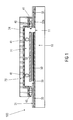
- Fig. 1 shows a sectional view through an organic photoelectric device according to a first embodiment of the present invention.
- the organic photoelectric device 100 has a substrate 10 including a surface 11. On the surface 11, a base electrode 30a, and an electrically insulated partial base electrode 30b is formed. Subsequently, a cover electrode 33 is formed, so that an organic functional layer 50 is arranged between the cover electrode 33 and the base electrode 30.
- the lateral extent of the organic functional layer 50 is equal, for example, to the lateral extent of the cover electrode or deviates only slightly therefrom.
- the base electrode 30a has a substrate metallization 31 on one of its edges on a surface facing away from the surface 11.
- the partial base electrode 30b has, on a surface facing away from the surface 11, a substrate metallization 32, which in its lateral dimensions corresponds, for example, to the partial base electrode 30b or deviates only slightly from it.
- An encapsulation adhesive 40 and electrically conductive adhesive 41 to which an electrically conductive coating 34 of a self-supporting cover member 20 adjoins, is arranged on a surface of the substrate metallization 32 facing the partial base electrode 30b.
- the self-supporting cover member 20 comprises a cavity 22, in which the layer stack of a part of the base electrode 30, the organic functional layer 50, and the cover electrode 33 is arranged.
- the substrate metallizations 31 and 32 as well as the base electrode 30 and the partial base electrode 30b adjoining the substrate metallizations 31 and 32 project laterally beyond the area encapsulated by the self-supporting cover member 20 so as to contact the substrate metallization 31, which may be formed as anode terminal 31, and the substrate metallization 32 , which may be formed as a cathode terminal 32 to allow.
- the electrically conductive coating 34 is electrically conductively connected to the cover electrode 33 by an electrically conductive adhesive 41, for example, at several points.
- the self-supporting cover member 20 may be formed, for example, as a cover glass 20, wherein not necessarily glass must be used as the material for the cover glass 20, but for example, a transparent plastic would be used, for example to realize flexible devices.
- the cavity 22 of the cover glass 20 can be etched, embossed or milled, for example, by a subtractive method in a plane glass.
- the electrically conductive coating 34 of the cover glass 20 may, for example, be designed as a cover glass metallization 34.
- a cover glass can also be referred to below as encapsulation glass or encapsulating glass.
- the metallization of the cover glass 20 or a coating of the cover glass 20 with another conductive material has the purpose of the cover glass metallization 34 or the coating 34 of the cover glass 20, for example via the Substratmetallmaschine 32 introduced stream by means of an electrically conductive adhesive 41 on the cover glass 20 lead or with the help of the cover glass 20, as a carrier of the cover glass metallization 34 to distribute the power evenly.
- the cover glass metallization 34 conducts the current to further contact points, which may be located at other locations of the edge region of the optical photoelectric device 100 or distributed over the entire surface of the cover glass 20 on.
- the distributed contact points in turn lead by means of electrically conductive adhesive 41, the current to the cover electrode 33.
- a uniform current distribution over the entire surface of the cover electrode 33 are made possible.
- the cover glass metallization 34 is connected to the cathode terminal 32 or to the substrate metallization 32 with an electrically conductive adhesive 41. This ensures that the inactive edge regions are minimized by the substrate metallization 32 only has the necessary width for encapsulation, and the current transport or the current distribution, however, takes place through the cover glass metallization 34 of the cover glass 20.
- the combination of encapsulation area and electrically conductive contact area on the substrate metallization 32 reduces the non-optically active edge area of the organic photoelectric component 100.
- the current is also conducted with electrically conductive adhesive 41 within the cavity 22 of the cover glass 20 on the cover electrode 33.
- electrically conductive adhesive 41 within the cavity 22 of the cover glass 20 on the cover electrode 33.
- the cover glass metallization 34 can be applied by printing processes, for example.
- the cavity 22 in the cover glass 20 is chamfered. Otherwise, the cavity edge may be provided with a paste or filler to allow metallization of the flank.
- the embodiments described herein are configured to emit light through the substrate.
- the self-supporting cover member 20 thus forms the back of the embodiments described herein and the substrate 10, the front of the embodiments described herein.
- the lateral extent of the organic functional layer 50 and of the surrounding electrodes determines the optically active surface of the organic photoelectric components.
- the base electrode 30 of the in Fig. 1 shown optical component 100 may have a metal network to reduce the resistance of the base electrode 30 and better power distribution.
- the first partial electrode 30a has, on a surface facing away from the surface 11, a substrate metallization 31 which corresponds in its lateral dimensions, for example, to those of the first partial electrode 30a or deviates only slightly therefrom.
- the second part-ground electrode 30b has, on a surface facing away from the surface 11, a substrate metallization 32, which in its lateral dimensions corresponds, for example, to the second part-ground electrode 30b or deviates only slightly from it.
- An encapsulation adhesive 40 and electrically conductive adhesive 41 to which an electrically conductive coating 34 of a self-supporting cover member 20 adjoins, are arranged on a surface of the substrate metallization 31 facing the first partial base electrode 30a.
- the self-supporting cover member 20 comprises a cavity 22, in which the layer stack of the base electrode 30, the organic functional layer 50, and the cover electrode 33 is arranged.
- the substrate metallizations 31 and 32 and the partial base electrodes 30a and 30b adjoining the substrate metallizations 31 and 32 project laterally beyond the area encapsulated by the self-supporting cover member 20 so as to contact the substrate metallization 31, which may be formed as anode terminal 31, and the substrate metallization 32, which may be formed as a cathode terminal 32 to allow.
- the cover electrode 33 is connected directly to the cathode terminal 32 or the substrate metallization 32 in an electrically conductive manner, for example via a conductive web.
- the cover glass metallization 34 is electrically conductively connected to the transparent base electrode 30.
- the cover electrode 33 and the organic functional layer 50 or the functional stack of the organic photoelectric component, such as an OLED, have electrically insulated plated-through holes for this purpose.
- electrically conductive adhesive 41 may be arranged for the electrically conductive connection of the cover glass metallization 33 to the base electrode 30.
- the current from the anode terminal 31 or the substrate metallization 31 is conducted by means of an electrically conductive adhesive 41 on the cover glass metallization 34 of the cover glass 20, which evenly distributes the current or electrically interconnects various active modules and then via further electrically conductive adhesive 41 leads to the transparent base electrode 30.
- the base electrode 30 and the first partial ground electrode 30a have a same potential.
- the electrically conductive adhesive 41 can also be replaced by an electrically conductive contact pin, for example.
- the plated-through holes can be arranged at locally laterally varying points of the cover electrode 33 and the organic functional layer 50, for example as bores. It should be noted that the plated-through holes do not impair the electrical conductivity of the cover electrode 33 and a function of the organic functional layer 50.
- the cover glass metallization 34 conducts the current to further contact points, which may be located at other locations of the edge area or distributed over the entire surface of the cover glass 20, which in turn conduct electricity to the base electrode 30 by means of electrically conductive adhesive 41.
- a uniform current distribution over the entire surface of the base electrode 30 can be made possible.
- optical component 200 is that due to the electrically conductive coupling of the conductive material 34 locally at varying locations with the base electrode 30 on a metal mesh in or on the base electrode 30 can be omitted to reduce the sheet resistance, thereby increasing the optical active area and in the embodiment of the organic photoelectric device 200 as a substrate emitter de optical impression and the luminous efficiency improved.
- Fig. 3 shows a sectional view through an organic photoelectric device 300 according to a third embodiment of the present invention.
- Organic photoelectric device 200 shown differs from that in FIG Fig. 1 shown organic photoelectric device 100, characterized in that instead of a cavity 22 provided with glass, a plane cavity-less glass substrate is used as a cover glass 20. Instead of producing the depressions or cavities by etching subtractive, an encapsulation edge is produced by means of structured melted glass frit paste at the edges of the cover glass 20, which distance between the coated substrate 100 required for the active layers or organic functional layer 50 and the placement of getter materials and the cover glass substrate or the cover glass 20 realized.
- Fig. 4 shows a sectional view through a photoelectric device 400 according to a fourth embodiment of the present invention.
- This in Fig. 4 shown organic photoelectric device 400 differs in Fig. 2 shown organic photoelectric device 200, analogous to the organic photoelectric devices 300 and 100, by the use of an additive method based on structured molten glass frit paste for the production of cavities.
- the encapsulation edge of the cover glass 20, that is, the recessed area of the cavities is also printed here, for example in the form of a paste of glass frits and then baked at suitable temperatures in the clear cover glass.
- Fig. 5 shows a sectional view through an organic photoelectric device 500 according to a fifth embodiment of the present invention.
- This in Fig. 5 shown organic photoelectric device 500 differs by the in Fig. 1 shown organic photoelectric device 100 by the use of a cover plate 21 made of sheet metal, instead of a cover glass as a self-supporting cover member.
- a cover plate 21 made of sheet metal instead of a cover glass as a self-supporting cover member.
- an electrically conductive cover plate 21 instead of an electrically non-conductive cover glass, an electrically conductive coating of the cover member is unnecessary.
- the electrically conductive cover plate 21 made of sheet metal is connected in addition to the encapsulation adhesive 40 with an electrically conductive adhesive 41 to the cathode terminal of the substrate metallization 32.
- the substrate metallization 32 only has the width necessary for the encapsulation, and the current transport or the current distribution, on the other hand, takes place through the cover plate 21.
- the electrically conductive adhesive 41 it is sufficient if it is applied only at the corners, possibly only at one corner, if the cathode connection surface of the substrate metallization 32 is located there.
- the current is conducted by means of the electrically conductive adhesive 41 or the conductive adhesive from the Substratmetallmaschine 32 on the cover plate 21 and from the cover plate 21 to the cover electrode 33.
- the electrically conductive cover plate 21 ensures an efficient distribution of the current on the surface or allows an electrical connection of various active modules on the substrate surface.
- a metallic cover plate 21 is particularly suitable for the mass production of large-area OLEDs or OPVZs, since the cover plates 21, for example, by deep drawing in large quantities can be made large and inexpensive. In addition, the time-consuming and polluting etching of the cover glass cavities 22 for the coverslips falls away. Furthermore, the use of a metal cover plate 21 offers better mechanical stability, since the fracture-sensitive glass substrate is enclosed by the metal cover 21.
- Fig. 6 shows a sectional view through an organic photoelectric device 600 according to a sixth embodiment of the present invention.
- This in Fig. 6 shown organic photoelectric device 600 differs by the in Fig. 2 shown organic photoelectric device 200 by the use of a cover plate 21 made of sheet metal, instead of a cover glass as a self-supporting cover member.
- a cover plate 21 made of sheet metal instead of a cover glass as a self-supporting cover member.
- an electrically conductive coating 34 of the self-supporting cover member is unnecessary.
- the cover plate 21 made of sheet metal is also here next to the encapsulation adhesive 40 with an electrically conductive adhesive 41 is connected to the anode terminal of the substrate metallization 31. The current is conducted with conductive adhesive 41 from the cover plate 21 onto the transparent base electrode 30.
- electrically insulated through-connection points are provided in the cover electrode 33 and in the organic functional layer 50, that is to say in the functional layer stack of the organic photoelectric component 600.
- the use of an electrically conductive cover plate 21 makes it possible to introduce the current only on one side or corner of the organic photoelectric component 600.
- the electrically conductive cover plate 21 ensures an efficient distribution of the current over the entire surface.
- the cover electrode 33 is electrically conductively connected directly to the second base part electrode 30b, that is, without an additional substrate metallization 32, thus forming the anode terminal.
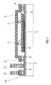
- Fig. 7 shows a sectional view through an organic photoelectric device 700 according to a seventh embodiment of the present invention.
- organic photoelectric device 500 is in the in Fig. 7 shown organic photoelectric device 700, a cover plate 21 made of sheet metal used as a self-supporting cover member.
- the cover plate 21 is electrically conductively connected to a cathode terminal.
- the cathode is connected directly to the cover plate 21, for example, by means of an electrically conductive contact pin 62 which is formed on a surface of the cover plate 21 facing away from the substrate 10.
- connection of the cathode can also be made directly to the electrically conductive cover plate 21, for example by soldering at any point of the cover plate 21. That is, the connection of the cathode takes place, contrary to the embodiments previously shown not via a Substratmetallmaschine.
- the anode is contacted via a contact pin 61 through a recess or bore in the cover plate 21 to the substrate metallization 31, which is formed on the base electrode 30.
- This recess / bore is expediently surrounded by a ring of encapsulation adhesive 40 in order to protect the organic functional layer 50 from environmental influences.
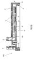
- FIG. 12 An exemplary application for this shows Figure 12 , Here, the non-emitting back side of an organic photoelectric device according to an embodiment of the present invention is shown.
- the recess 12 in the form of a bore which represents the contact point of the anode metallization 31, is embodied herein only at a corner 2 of the element.
- the contacting of the cathode 62 can be done at any other location of the cover plate 21.
- an anode contact can be realized at two opposite corners 2 and 4, since the Contact pin 61 can be used simultaneously as an adjusting element, in particular, if several OLED / OPVZ elements or organic photoelectric devices are to be strung together.
- recesses 12 for contacting the anode metallization 31 at all corners.
- recesses 12 may be present at all corners, but only a portion of the recesses 12 allow a contacting of the anode metallization 31, while the other part is used only for adjusting the organic photoelectric devices.
- the contact pin 61 Since the contact pin 61 is used for the adjustment of the device on the ground, the contact pin 61 inevitably touches the encapsulation plate or the cover plate 21. For this reason, to provide electrical insulation between the contact pin 61 and the cover plate 21 and the sheet. This can for example be done via a non-conductive ring which is mounted in the recess 12 and around the contact pin 61 and fits exactly into the recess 12 of the encapsulation sheet or the cover plate 21.
- the ring may consist of encapsulating adhesive 40, for example.
- the contact pin 61 to consist of an electrically conductive core which contacts the contact surface of the substrate metallization 31 and of an insulating jacket which touches the edge of the recess 12 in the encapsulation sheet or the cover plate 21.
- the improved mechanical stability provided by the metal top plate is further improved by the use of these contact pins 61, since this additionally enables simple electrical contacting and mechanical fastening.
- the contact pin 61 is formed as anode contact to contact the base electrode 30 and the cover plate 21 is connected to a cathode to contact the cover electrode 33
- a contact pin 62 as cathode contacts is formed to contact the lid electrode 33 and the cover plate 21 is connected to an anode to contact the base electrode 30.
- Fig. 8 shows a sectional view through an organic photoelectric device 800 according to an eighth embodiment of the present invention.
- organic photoelectric device 600 is the self-supporting Cover member in which in Fig. 8 shown organic photoelectric device 800 as a cover plate 21 made of sheet metal.
- This in Fig. 8 shown organic photoelectric device 800 differs by the in Fig. 6 shown photoelectric element 600 characterized in that the connection of the anode directly on the cover plate 21, for example by means of a contact pin 61 and not via a Substratmetallmaschine.
- the cover plate 21 leads, as already in the in Fig.
- Fig. 6 shown organic photoelectric device 600, the current via electrically conductive adhesive 41 directly to the transparent base electrode 30, for which in the functional layer stack or in the cover electrode 33 and the organic functional layer 50 of the OLED / OPVZ or the organic photoelectric device 800 electrically insulated via-connection points are provided.
- the cathode via a contact pin 62 comparable to the contact pin 61, according to Fig. 7 , contacted by a recess or bore in the cover plate 21 on the substrate metallization 32.
- the substrate metallization 32 is furthermore, as already shown in the second, fourth embodiment, connected directly to the cover electrode 33 and formed on a side facing away from the substrate 10, a partial base electrode 30b.
- the recess or bore for the passage of the contact pin 62 in the cover electrode 21 may be realized in one or more corners of the cover plate 21 and is preferably surrounded between the substrate 10 and the cover plate 21 with a ring of encapsulating adhesive 40.
- Fig. 9 shows a sectional view through an organic photoelectric device 900 according to a ninth embodiment of the present invention.
- This in Fig. 9 shown organic photoelectric device 900 differs by the in Fig. 7 shown organic photoelectric device 700 characterized in that the cover plate 21 made of sheet metal at its edges has a collar 24 which has been produced for example by deep drawing. As a result, the cover plate 21 forms a trough, in which the coated OLED / OPVZ substrate 10 is inserted and glued.
- the collar 24 of the cover plate 21 serves as an encapsulation surface, on which the encapsulation adhesive 40 is applied in order to protect the organic functional layer from environmental influences.
- the encapsulating adhesive is applied between the collar 24 of the cover plate 21 and end faces 14 of the substrate 10 and thus seals the space enclosed by the cover plate 21 from environmental influences. This largely eliminates the area required for the encapsulation on the substrate surface 11, whereby the inactive edge region of the organic photoelectric device 900 is further minimized.
- the contacting of the cathode, for example by means of a contact pin 62 is analogous to the seventh embodiment directly on the cover plate 21, wherein the current is conducted via conductive adhesive 41 to the cover electrode 33.
- the anode on the other hand is contacted via a contact pin 61 through a recess or bore in the cover plate 21 to the Substratmetallmaschine 31 analogous to the seventh embodiment.
- the recess or bore for the passage of the contact pin 61 may be realized in one or more corners of the cover plate 21 and may preferably be surrounded between substrate 10 and cover plate 21 with a ring of encapsulating adhesive 40.
- Fig. 10 shows a sectional view through an organic photoelectric device 1000 according to a tenth embodiment of the present invention.
- This in Fig. 10 shown organic photoelectric device 1000 differs by the in Fig. 8 shown organic photoelectric device 800 characterized in that the cover electrode 33, as in the in Figure 6 shown organic photoelectric device 600 directly to the second part of the base electrode 30b, that is electrically conductively connected without an additional Substratmetallmaschine 32 and above all further characterized in that the cover plate 21 made of sheet metal at its edges has a collar 24 which has been produced for example by deep drawing. As a result, the cover plate 21 forms a trough, in which the coated OLED / OPVZ substrate 10 is inserted and glued.
- the collar 24 of the cover plate 21 serves as an encapsulation surface, on which the encapsulation adhesive 40 is applied.
- the encapsulating adhesive is applied between the collar 24 of the cover plate 21 and end faces 14 of the substrate 10 and thus seals the space enclosed by the cover plate 21 from environmental influences. This largely eliminates the area required for the encapsulation on the substrate surface 11, whereby the inactive edge region of the organic photoelectric device 1000 is minimized.
- the contacting of the anode, for example by means of a contact pin 61 is analogous to the eighth embodiment directly on the cover plate 21, wherein the current is passed over conductive adhesive 41 directly to the transparent base electrode 30, for which in the functional layer stack or in the cover electrode 33 and the organic functional layer 50 of the OLED / OPVZ or the organic photoelectric device 1000 electrically insulated via-connection points are provided.
- the cathode is contacted analogously to the eighth embodiment via a contact pin 62 through a recess or bore in the cover plate on the substrate metallization 32.
- the recess or bore for the passage of the contact pin 61 can be realized in one or more corners of the cover plate 21 and preferably between substrate 10 and the cover plate 21 with a ring of encapsulating adhesive 40 to be surrounded.
- FIG. 10 is a sectional view of an organic photoelectric device 1100 according to an eleventh embodiment of the present invention.
- the organic photoelectric device 1000 shown in FIG Fig. 11 shown organic photoelectric device 1100 contact pins 61, 62, the solid are connected to the cover plate 21. This can be realized by the contact pins 61, 62, for example, pressed or glued.
- the contact pins 61, 62 or the pins have, for example, an electrically conductive core 64, for example made of metal, and an electrically insulating sheath 66.
- the conductive core 64 is connected, for example, with a conductive adhesive to the contact surfaces (so-called "contact pads") on the OLED / OPVZ substrate 10, that is, the conductive core 64 of at least one first contact pin 61, 62 is connected to the cover plate 21, which is electrically conductively coupled to the base electrode 30 or the cover electrode 33, and a conductive core 64 of at least one second contact pin 61, 62 is connected to a substrate metallization 31, 32 which is electrically conductively coupled to the cover electrode 33 or the base electrode 30, wherein the electrically insulating sheath 66 of the second contact pin 61, 62 comes into contact with the cover plate.
- a conductive adhesive to the contact surfaces (so-called "contact pads") on the OLED / OPVZ substrate 10
- the conductive core 64 of at least one first contact pin 61, 62 is connected to the cover plate 21, which is electrically conductively coupled to the base electrode 30 or the cover electrode 33
- an internal thread 68 may be designed, whereby a simple assembly of the device or the organic photoelectric device 1100 is possible.
- the electrically conductive core 64 may also be designed as a permanent magnet in which it consists of a magnetized material.
- the organic photoelectric devices are formed as a substrate emitter, it is also conceivable that the conductive coating of the self-supporting cover member and the self-supporting cover member for the Nutzwellenat organic photoelectric devices are transparent and embodiments are formed as a substrate absorber.
- the electrically conductive material may be electrically conductively coupled to the cover electrode and the self-supporting cover member, another of the cover electrode and the electrically conductively coupled to the cover electrode material, electrically insulated electrically conductive material.
- the further electrically conductive material may, for example, be electrically conductively coupled via plated-through holes isolated from the cover electrode and the organic functional layer to the base electrode.
- the conductive self-supporting cover member may comprise two electrically conductive materials separated by electrical insulation layers.
- the self-supporting cover member may have locally electrically laterally distributed locations electrically insulated conductive materials, preferably the locations are electrically coupled to each other which electrically conductively couple the same electrode.
- a strip arrangement of the two electrically conductive materials is conceivable.
- Another embodiment of the present invention may be formed as an organic light-emitting diode or an organic solar cell consisting of substrates, ground electrode, organic layers, cover electrode and encapsulation, which is provided in the encapsulation glass with metallic interconnects and adhered to the OLED / OPVZ substrate ,
- the metal conducting paths on this encapsulation glass are connected, for example, by means of an electrically conductive adhesive, both with the lid electrode of the OLED / OPVZ, to the edge contact surfaces on the substrate, and the encapsulating glass is provided with a rushed or milled cavity.
- Another embodiment of the present invention may be formed as an organic light-emitting diode or an organic solar cell consisting of substrates, ground electrode, organic layers, cover electrode and encapsulation, which is provided in the encapsulation glass with metallic interconnects and adhered to the OLED / OPVZ substrate ,
- the metal interconnects on this encapsulation glass are connected to the substrate, for example, by means of an electrically conductive adhesive, both with the base electrode of the OLED / OPVZ via a via electrically insulated from the cover electrode and with the edge contact surfaces.
- the encapsulating glass is provided with an etched or milled cavity.
- Another embodiment of the present invention may be formed as an organic light-emitting diode or organic solar cell consisting of a substrate, ground electrode, organic layers, cover electrode and encapsulation, which is provided in the encapsulation glass with metallic interconnects and adhered to the OLED / OPVZ substrate ,
- the metal interconnects on this encapsulation glass are connected, for example, by means of an electrically conductive adhesive, both to the cover electrode of the OLED / OPVZ, and to the edge contact surfaces on the substrate.
- the encapsulating glass consists of a planar substrate.
- the cavity, a surface depression of the encapsulating glass, is produced by a glass frit frame, which is applied to the substrate to be provided with encapsulation adhesive contact with the substrate and encapsulated before the encapsulation by means of a suitable printing process.
- Another embodiment of the present invention may be embodied as an organic light-emitting diode or organic solar cell consisting of substrate, base electrode, organic layers, cover electrode and encapsulation glass, which is provided with an encapsulating glass with metallic interconnects and glued on the OLED / OPVZ substrate.
- the metal conducting paths on this encapsulation glass are connected, for example, by means of an electrically conductive adhesive, both to the base electrode of the OLED / OPVZ via a through-connection electrically insulated from the cover electrode, ie also to the edge contact surfaces on the substrate.
- the encapsulating glass consists of a planar substrate.
- the cavity, a flat depression of the encapsulating glass is produced by a glass frit frame, which is applied by means of a substrate before the encapsulation by means of a suitable printing process to be provided with encapsulation adhesive pads and baked.
- a further embodiment of the present invention may be embodied as an OLED / OPVZ emitting or absorbing the substrate, consisting of substrates, transparent base electrode, organic layers, cover electrode and encapsulation, which adheres a metal encapsulation element to the OLED / OPVZ substrate and for electrical contacting, both with the cover electrode of the OLED / OPVZ and with an external power supply or control electronics.
- Embodiments of the present invention in which an encapsulation element is made of metal may have recesses and bores at the corners, which are enclosed with encapsulation adhesive, and allow a contacting of the base electrode of the OLED / OPVZ with an external power supply or control electronics that is electrically isolated from the encapsulation element.
- a further embodiment of the present invention may be embodied as a substrate emitting / absorbing OLED / OPVZ comprising substrate, ground electrode, organic layers, cap electrode and encapsulation adhered to a metal encapsulation element on the OLED / OPVZ substrate, and for electrical contacting both with the base electrode or OLED / OPVZ via an electrically insulated from the cover electrode via hole, as well as with an external power supply or control electronics.
- Embodiments of the present invention which is a metal encapsulation element, may have at the corners recesses or bores enclosed by encapsulation adhesive and electrically insulated from the encapsulation element Contacting with the cover electrode of the OLED / OPVZ with an external power supply or control electronics.
- the encapsulation element may serve to mechanically secure the OLED / OPVZ element.
- the encapsulation element may be in the form of a trough made of, for example, a deep-drawn sheet metal, in which the substrate is located, and glued to the substrate at least at the lateral end faces of the substrate.
- the encapsulation element may be made of magnetic metal sheet, which can be used for mechanical fixation of the OLED / OPVZ element.
- the encapsulation element may be curved and made of magnetic metal sheet, whereby in conjunction with the use of flexible substrates, such as transparent films or thin glass as OLED / OPVZ substrate, a bent OLED / OPVZ element or organic photoelectric Component can be produced, so that the OLED / OPVZ is mounted on the encapsulation element in an application device.
- flexible substrates such as transparent films or thin glass as OLED / OPVZ substrate
- a bent OLED / OPVZ element or organic photoelectric Component can be produced, so that the OLED / OPVZ is mounted on the encapsulation element in an application device.
- the encapsulation element can be embodied as an encapsulation glass, wherein the encapsulation glass ideally has a size identical to the substrate and has holes at the corners, which make it possible to contact the contact surfaces on the substrate.
- a contact pin can be introduced into the contacting bore or contacting holes of the encapsulation element, which allows a simple contacting of the device or the electrode terminals and consists of an electrically conductive material.
- the introduced into the Kunststoffssensbohrung or Kunststofftechnikslöcher of the encapsulation element contact pin may for example comprise an electrically conductive core and an insulating sheath, further, the contact pin may be designed as a permanent magnet and, for example, have an internal thread.
- the cover glass similar to the substrate with a metallization, is provided with cover glass metallization.
- This has the purpose to guide the current introduced to the metallization of the cover glass by means of an electrically conductive adhesive on the cover glass.
- the cover glass metallization conducts the current to other contact points, which may be located at the other locations of the edge area or distributed over the entire surface of the cover glass, which in turn conduct the current by means of electrically conductive adhesive to the cover electrode or the base electrode.
- cover glass metallization conducts the current to other contact points, which may be located at the other locations of the edge area or distributed over the entire surface of the cover glass, which in turn conduct the current by means of electrically conductive adhesive to the cover electrode or the base electrode.
- cover element for example an encapsulation sheet made of metal, or another conductive material can be used.
- the metal encapsulation element serves as a contact element for the cathode or the anode, depending on the design of the device or the organic photoelectric device.
- the encapsulation sheet preferably has holes / holes at the corners. About these holes, the contacting of the substrate can be realized via a contact pin.
- the contact pin can either be firmly connected to the substrate / encapsulation element or introduced from the outside.
- this contact pin is preferably magnetic or has a bore with internal thread.
- this is preferably designed conical so that when placing an OLED / OPVZ device in a holder, which is provided with holes that have a bevel corresponding to the conical pin allow a self-positioning of the device.
- Embodiments of the present invention thus make it possible to reduce non-luminous or optically non-active regions of an organic photoelectric component or an OLED / OPVZ by minimizing edge areas of the individual OLED or OPVZ elements by a combination of contact and encapsulation surfaces, thus allowing the production of large illuminated areas or optically active areas with a high degree of filling.
- the encapsulation with alternatives or structured encapsulation substrates shown in the exemplary embodiments shown enables large-area OLEDs / OPVZ elements with minimal inactive edge areas required for encapsulation and contacting.
- embodiments of the invention make it possible to dispense with coverslips having cavities which are complicated to produce and which can thereby be produced more cheaply and thus more environmentally friendly overall in larger quantities.
- embodiments of the present invention are characterized by a simple contacting of OLED / OPVZ elements and easier mounting / mounting and handling of the OLED / OPVZ elements due to greater mechanical stability of the device. This generally leads to a greater robustness of the OLED / OPVZ elements.
Landscapes
- Physics & Mathematics (AREA)
- Optics & Photonics (AREA)
- Electromagnetism (AREA)
- Electroluminescent Light Sources (AREA)
- Photovoltaic Devices (AREA)
Applications Claiming Priority (1)
| Application Number | Priority Date | Filing Date | Title |
|---|---|---|---|
| DE102009046755A DE102009046755A1 (de) | 2009-11-17 | 2009-11-17 | Organisches photoelektrisches Bauelement |
Publications (2)
| Publication Number | Publication Date |
|---|---|
| EP2323191A2 true EP2323191A2 (fr) | 2011-05-18 |
| EP2323191A3 EP2323191A3 (fr) | 2011-12-28 |
Family
ID=43587571
Family Applications (1)
| Application Number | Title | Priority Date | Filing Date |
|---|---|---|---|
| EP20100191333 Withdrawn EP2323191A3 (fr) | 2009-11-17 | 2010-11-16 | Composant photoélectrique organique |
Country Status (4)
| Country | Link |
|---|---|
| US (1) | US8530924B2 (fr) |
| EP (1) | EP2323191A3 (fr) |
| JP (1) | JP2011108651A (fr) |
| DE (1) | DE102009046755A1 (fr) |
Cited By (2)
| Publication number | Priority date | Publication date | Assignee | Title |
|---|---|---|---|---|
| WO2013131828A1 (fr) * | 2012-03-08 | 2013-09-12 | Osram Opto Semiconductors Gmbh | Composant optoélectronique organique et procédé de fabrication d'un composant optoélectronique organique |
| EP3035406A1 (fr) * | 2014-12-16 | 2016-06-22 | LG Display Co., Ltd. | Dispositif électroluminescent organique |
Families Citing this family (34)
| Publication number | Priority date | Publication date | Assignee | Title |
|---|---|---|---|---|
| TWI577071B (zh) * | 2010-08-24 | 2017-04-01 | 友達光電股份有限公司 | 有機發光二極體封裝結構及其製造方法 |
| US9188323B2 (en) * | 2010-10-20 | 2015-11-17 | Semiconductor Energy Laboratory Co., Ltd. | Lighting device |
| JP5997758B2 (ja) * | 2011-03-29 | 2016-09-28 | エルジー ディスプレイ カンパニー リミテッド | 有機電子装置の製造方法 |
| FR2976730B1 (fr) * | 2011-06-17 | 2013-12-06 | Astron Fiamm Safety | Delo encapsulee en colle pleine plaque avec un capot troue |
| DE102011107642A1 (de) * | 2011-07-12 | 2013-01-17 | Bjb Gmbh & Co. Kg | Leuchtmittel mit wenigstens einer organischen, Licht emittierenden Diode |
| DE102011079014A1 (de) * | 2011-07-12 | 2013-01-17 | Ledon Oled Lighting Gmbh & Co. Kg | Leuchtmodul mit reduziertem Flächenbedarf |
| US9515284B2 (en) | 2011-07-27 | 2016-12-06 | Panasonic Intellectual Property Management Co., Ltd. | Organic electroluminescence element and production method therefor |
| KR102001815B1 (ko) * | 2011-11-29 | 2019-07-19 | 가부시키가이샤 한도오따이 에네루기 켄큐쇼 | 밀봉체의 제작 방법 및 발광 장치의 제작 방법 |
| US20150041783A1 (en) * | 2012-02-13 | 2015-02-12 | Panasonic Corporation | Organic electroluminescence element |
| DE102012207229B4 (de) * | 2012-05-02 | 2020-06-04 | Osram Oled Gmbh | Elektronisches Bauelement und Verfahren zum Herstellen eines elektronischen Bauelements |
| KR101514114B1 (ko) * | 2012-09-14 | 2015-04-21 | 주식회사 엘지화학 | Oled 조명 모듈 |
| DE102012109141A1 (de) * | 2012-09-27 | 2014-03-27 | Osram Opto Semiconductors Gmbh | Optoelektronisches Bauelement und Verfahren zum Herstellen eines optoelektronischen Bauelementes |
| WO2014136359A1 (fr) | 2013-03-07 | 2014-09-12 | ローム株式会社 | Cellule solaire à film mince organique ainsi que procédé de fabrication de celle-ci, et appareil électronique |
| JP2014192188A (ja) * | 2013-03-26 | 2014-10-06 | Rohm Co Ltd | 有機薄膜太陽電池およびその製造方法、および電子機器 |
| JP2014175380A (ja) * | 2013-03-07 | 2014-09-22 | Rohm Co Ltd | 有機薄膜太陽電池およびその製造方法 |
| JP6082294B2 (ja) * | 2013-03-26 | 2017-02-15 | ローム株式会社 | 有機薄膜太陽電池およびその製造方法、および電子機器 |
| JP6213984B2 (ja) * | 2013-06-17 | 2017-10-18 | 国立研究開発法人産業技術総合研究所 | 有機el発光ダイオード及び有機el照明装置 |
| JP6061301B2 (ja) * | 2013-06-17 | 2017-01-18 | 国立研究開発法人産業技術総合研究所 | フレキシブル有機el表示装置及びその製造方法 |
| DE102013111739B4 (de) * | 2013-10-24 | 2024-08-22 | Pictiva Displays International Limited | Optoelektronisches Bauelement und Verfahren zum Herstellen eines optoelektronischen Bauelements |
| DE102013111732A1 (de) * | 2013-10-24 | 2015-04-30 | Osram Oled Gmbh | Optoelektronisches Bauelement, optoelektronische Baugruppe, Verfahren zum Herstellen eines optoelektronischen Bauelements und Verfahren zum Herstellen einer optoelektronischen Baugruppe |
| CN104022145B (zh) * | 2014-06-23 | 2017-01-25 | 深圳市华星光电技术有限公司 | 基板的封装方法及封装结构 |
| JP2016051805A (ja) * | 2014-08-29 | 2016-04-11 | ローム株式会社 | 有機薄膜太陽電池およびその製造方法、電子機器 |
| CN104299981B (zh) * | 2014-09-22 | 2017-02-08 | 京东方科技集团股份有限公司 | Oled显示面板及其封装方法和oled显示装置 |
| JP6485679B2 (ja) * | 2014-09-24 | 2019-03-20 | 日本精機株式会社 | 有機elパネル及びその製造方法 |
| DE102014116740A1 (de) * | 2014-11-17 | 2016-05-19 | Emdedesign Gmbh | Leuchte umfassend wenigstens zwei OLED-Leuchtmittel |
| DE102014223367A1 (de) | 2014-11-17 | 2016-05-19 | Osram Oled Gmbh | Organische Leuchtiode, organisches Leuchtmodul und Verfahren zur Herstellung einer organischen Leuchtiode |
| CN104617234A (zh) * | 2015-02-13 | 2015-05-13 | 京东方科技集团股份有限公司 | 隔垫物、有机电致发光显示面板、制作方法及显示装置 |
| KR101805552B1 (ko) * | 2015-08-31 | 2017-12-08 | 엘지디스플레이 주식회사 | 유기발광 표시장치 |
| KR102466959B1 (ko) | 2015-12-31 | 2022-11-11 | 엘지디스플레이 주식회사 | 유기 발광 표시 장치 |
| DE102017105946A1 (de) | 2017-03-20 | 2018-09-20 | Osram Oled Gmbh | Optoelektronisches Bauelement und Verfahren zur Herstellung eines optoelektronischen Bauelements |
| CN107482041B (zh) * | 2017-08-16 | 2020-04-24 | 武汉天马微电子有限公司 | 柔性显示面板与柔性显示装置 |
| US10849235B1 (en) * | 2020-05-20 | 2020-11-24 | Tactotek Oy | Method of manufacture of a structure and structure |
| CN114551755B (zh) * | 2022-02-08 | 2025-01-28 | 深圳市华星光电半导体显示技术有限公司 | 一种显示面板及移动终端 |
| JP2023170819A (ja) * | 2022-05-20 | 2023-12-01 | パナソニックホールディングス株式会社 | 太陽電池モジュールおよび太陽電池モジュールの製造方法 |
Citations (4)
| Publication number | Priority date | Publication date | Assignee | Title |
|---|---|---|---|---|
| US20030197475A1 (en) * | 2002-04-04 | 2003-10-23 | Makoto Takamura | Flat-panel display, manufacturing method thereof, and portable terminal |
| WO2008062645A1 (fr) * | 2006-11-21 | 2008-05-29 | Konica Minolta Holdings, Inc. | Panneau électroluminescent organique et élément de scellement |
| EP1939952A2 (fr) * | 2006-12-28 | 2008-07-02 | Yamagata Promotional Organization for Industrial Technology | Appareil électroluminescent EL organique et son procédé de fabrication |
| JP2008186618A (ja) * | 2007-01-26 | 2008-08-14 | Matsushita Electric Works Ltd | 有機エレクトロルミネッセンス発光装置 |
Family Cites Families (16)
| Publication number | Priority date | Publication date | Assignee | Title |
|---|---|---|---|---|
| JP3290584B2 (ja) * | 1996-02-07 | 2002-06-10 | パイオニア株式会社 | 有機エレクトロルミネセンス素子 |
| DE69817505T2 (de) | 1997-05-22 | 2004-06-17 | Koninklijke Philips Electronics N.V. | Organische elektrolumineszente vorrichtung |
| JP4066547B2 (ja) * | 1999-01-25 | 2008-03-26 | 松下電器産業株式会社 | 表示装置 |
| JP2000243559A (ja) * | 1999-02-18 | 2000-09-08 | Kawaguchiko Seimitsu Co Ltd | エレクトロルミネッセンス |
| JP2001052858A (ja) | 1999-08-05 | 2001-02-23 | Futaba Corp | 有機el表示装置 |
| JP2001223079A (ja) | 2000-02-09 | 2001-08-17 | Futaba Corp | 有機el表示素子 |
| JP2002008856A (ja) | 2000-06-27 | 2002-01-11 | Nippon Seiki Co Ltd | 有機elパネル |
| JP2002280167A (ja) * | 2001-03-16 | 2002-09-27 | Pioneer Electronic Corp | 有機el表示パネル |
| KR20040052240A (ko) * | 2001-10-18 | 2004-06-22 | 코닌클리케 필립스 일렉트로닉스 엔.브이. | 전자 발광 디바이스 |
| JP2005078906A (ja) | 2003-08-29 | 2005-03-24 | Nippon Seiki Co Ltd | 有機elパネル |
| TWI362231B (en) | 2003-11-21 | 2012-04-11 | Semiconductor Energy Lab | Display device |
| JP4780950B2 (ja) | 2003-11-21 | 2011-09-28 | 株式会社半導体エネルギー研究所 | 表示装置 |
| KR100707157B1 (ko) * | 2003-12-27 | 2007-04-13 | 삼성에스디아이 주식회사 | 유기발광소자 및 그 제조방법 |
| JP2009503777A (ja) | 2005-07-27 | 2009-01-29 | コーニンクレッカ フィリップス エレクトロニクス エヌ ヴィ | 駆動回路が一体化された封止部を有する照明装置 |
| JP2008300101A (ja) * | 2007-05-30 | 2008-12-11 | Nippon Seiki Co Ltd | 有機elパネル及びその製造方法 |
| JP2009217984A (ja) * | 2008-03-07 | 2009-09-24 | Rohm Co Ltd | 有機el装置 |
-
2009
- 2009-11-17 DE DE102009046755A patent/DE102009046755A1/de not_active Withdrawn
-
2010
- 2010-11-16 EP EP20100191333 patent/EP2323191A3/fr not_active Withdrawn
- 2010-11-16 US US12/947,621 patent/US8530924B2/en not_active Expired - Fee Related
- 2010-11-17 JP JP2010257294A patent/JP2011108651A/ja active Pending
Patent Citations (4)
| Publication number | Priority date | Publication date | Assignee | Title |
|---|---|---|---|---|
| US20030197475A1 (en) * | 2002-04-04 | 2003-10-23 | Makoto Takamura | Flat-panel display, manufacturing method thereof, and portable terminal |
| WO2008062645A1 (fr) * | 2006-11-21 | 2008-05-29 | Konica Minolta Holdings, Inc. | Panneau électroluminescent organique et élément de scellement |
| EP1939952A2 (fr) * | 2006-12-28 | 2008-07-02 | Yamagata Promotional Organization for Industrial Technology | Appareil électroluminescent EL organique et son procédé de fabrication |
| JP2008186618A (ja) * | 2007-01-26 | 2008-08-14 | Matsushita Electric Works Ltd | 有機エレクトロルミネッセンス発光装置 |
Cited By (5)
| Publication number | Priority date | Publication date | Assignee | Title |
|---|---|---|---|---|
| WO2013131828A1 (fr) * | 2012-03-08 | 2013-09-12 | Osram Opto Semiconductors Gmbh | Composant optoélectronique organique et procédé de fabrication d'un composant optoélectronique organique |
| US9196866B2 (en) | 2012-03-08 | 2015-11-24 | Osram Opto Semiconductors Gmbh | Organic optoelectronic device and method for producing an organic optoelectronic device |
| DE102012203637B4 (de) | 2012-03-08 | 2020-06-04 | Osram Oled Gmbh | Organisches optoelektronisches Bauelement und Verfahren zur Herstellung eines organischen optoelektronischen Bauelements |
| EP3035406A1 (fr) * | 2014-12-16 | 2016-06-22 | LG Display Co., Ltd. | Dispositif électroluminescent organique |
| US10021760B2 (en) | 2014-12-16 | 2018-07-10 | Lg Display Co., Ltd. | Organic light emitting display device |
Also Published As
| Publication number | Publication date |
|---|---|
| US8530924B2 (en) | 2013-09-10 |
| DE102009046755A1 (de) | 2011-05-26 |
| US20110121352A1 (en) | 2011-05-26 |
| EP2323191A3 (fr) | 2011-12-28 |
| JP2011108651A (ja) | 2011-06-02 |
Similar Documents
| Publication | Publication Date | Title |
|---|---|---|
| EP2323191A2 (fr) | Composant photoélectrique organique | |
| EP2732483A1 (fr) | Module lumineux d'encombrement réduit | |
| EP2625731A1 (fr) | Élément d'éclairage comprenant des modules delo | |
| EP2316143B1 (fr) | Diode électroluminescente organique (delo) et procédé de production d'une delo | |
| EP2529604B1 (fr) | Source lumineuse sur une carte imprimée et arrangement de sources lumineuses | |
| DE102007004509A1 (de) | Beleuchtungselement und Verfahren zu seiner Herstellung | |
| DE102014103747B4 (de) | Optoelektronisches Bauelement und Verfahren zum Herstellen eines optoelektronischen Bauelements | |
| DE102006016373A1 (de) | Großflächige OLED's mit homogener Lichtemission | |
| WO2010034435A1 (fr) | Composant photo-électrique organique et procédé de réalisation d'un composant photo-électrique organique | |
| DE102014119539A1 (de) | Organisches optoelektronisches Bauelement und Verfahren zum Herstellen eines organischen optoelektronischen Bauelements | |
| DE102013106815A1 (de) | Optoelektronisches Bauelement und Verfahren zum Herstellen eines optoelektronischen Bauelementes | |
| DE102015102520B4 (de) | Optoelektronisches Bauelement und Verfahren zum Herstellen eines optoelektronischen Bauelements | |
| DE102014100747A1 (de) | Optoelektronische Bauelemente und Verfahren zum Herstellen optoelektronischer Bauelemente | |
| DE102006059168B4 (de) | Optoelektronische Vorrichtung und Verfahren zur Herstellung einer optoelektronischen Vorrichtung | |
| EP2834862B1 (fr) | Dispositif émetteur de lumière comprenant un élément oled | |
| WO2016042042A1 (fr) | Module optoélectronique et procédé de fabrication d'un module optoélectronique | |
| DE102015116055B4 (de) | Flächiges lichtemittierendes Bauelement und Verfahren zum Herstellen eines flächigen lichtemittierenden Bauelements | |
| WO2008083671A1 (fr) | Dispositif optoélectronique et procédé de fabrication d'un dispositif optoélectronique | |
| DE102012214216A1 (de) | Organisches Leuchtdiodenmodul und Verfahren zu dessen Herstellung | |
| DE102015118417A1 (de) | Optoelektronisches Bauelement und Verfahren zum Herstellen eines optoelektronischen Bauelements | |
| DE102012109141A1 (de) | Optoelektronisches Bauelement und Verfahren zum Herstellen eines optoelektronischen Bauelementes | |
| DE102012109208B4 (de) | Verfahren zum Bearbeiten einer Vorrichtung mit wenigstens einer elektrischen Schichtenstruktur und Bauelementanordnung hierfür | |
| DE112015003561B4 (de) | Organisches Bauteil | |
| DE102014103751A1 (de) | Organisches strahlungsemittierendes Bauelement | |
| DE102017114248A1 (de) | Organisches, lichtemittierendes bauelement und verfahren zum herstellen des organischen, lichtemittierenden bauelements |
Legal Events
| Date | Code | Title | Description |
|---|---|---|---|
| PUAI | Public reference made under article 153(3) epc to a published international application that has entered the european phase |
Free format text: ORIGINAL CODE: 0009012 |
|
| AK | Designated contracting states |
Kind code of ref document: A2 Designated state(s): AL AT BE BG CH CY CZ DE DK EE ES FI FR GB GR HR HU IE IS IT LI LT LU LV MC MK MT NL NO PL PT RO RS SE SI SK SM TR |
|
| AX | Request for extension of the european patent |
Extension state: BA ME |
|
| PUAL | Search report despatched |
Free format text: ORIGINAL CODE: 0009013 |
|
| AK | Designated contracting states |
Kind code of ref document: A3 Designated state(s): AL AT BE BG CH CY CZ DE DK EE ES FI FR GB GR HR HU IE IS IT LI LT LU LV MC MK MT NL NO PL PT RO RS SE SI SK SM TR |
|
| AX | Request for extension of the european patent |
Extension state: BA ME |
|
| RIC1 | Information provided on ipc code assigned before grant |
Ipc: H01L 51/44 20060101ALI20111122BHEP Ipc: H01L 51/52 20060101AFI20111122BHEP |
|
| 17P | Request for examination filed |
Effective date: 20120529 |
|
| 17Q | First examination report despatched |
Effective date: 20130913 |
|
| STAA | Information on the status of an ep patent application or granted ep patent |
Free format text: STATUS: THE APPLICATION IS DEEMED TO BE WITHDRAWN |
|
| 18D | Application deemed to be withdrawn |
Effective date: 20151117 |