EP2325830A1 - Affichage à diode électroluminescente organique, son procédé de commande et son unité de pixels - Google Patents
Affichage à diode électroluminescente organique, son procédé de commande et son unité de pixels Download PDFInfo
- Publication number
- EP2325830A1 EP2325830A1 EP10164582A EP10164582A EP2325830A1 EP 2325830 A1 EP2325830 A1 EP 2325830A1 EP 10164582 A EP10164582 A EP 10164582A EP 10164582 A EP10164582 A EP 10164582A EP 2325830 A1 EP2325830 A1 EP 2325830A1
- Authority
- EP
- European Patent Office
- Prior art keywords
- emitting diode
- light emitting
- organic light
- pixel
- transistor
- Prior art date
- Legal status (The legal status is an assumption and is not a legal conclusion. Google has not performed a legal analysis and makes no representation as to the accuracy of the status listed.)
- Withdrawn
Links
- 238000000034 method Methods 0.000 title claims abstract description 31
- 239000003086 colorant Substances 0.000 claims abstract description 16
- 238000009826 distribution Methods 0.000 claims abstract description 12
- 239000003990 capacitor Substances 0.000 claims description 13
- 230000001360 synchronised effect Effects 0.000 claims description 4
- 230000000875 corresponding effect Effects 0.000 claims 8
- 230000001276 controlling effect Effects 0.000 claims 3
- 230000000694 effects Effects 0.000 abstract description 3
- 238000010586 diagram Methods 0.000 description 22
- 238000004904 shortening Methods 0.000 description 7
- 238000005516 engineering process Methods 0.000 description 6
- 230000006870 function Effects 0.000 description 6
- 230000015556 catabolic process Effects 0.000 description 3
- 238000006731 degradation reaction Methods 0.000 description 3
- 239000000463 material Substances 0.000 description 3
- 239000011368 organic material Substances 0.000 description 3
- 230000004913 activation Effects 0.000 description 2
- 238000006243 chemical reaction Methods 0.000 description 2
- 230000007246 mechanism Effects 0.000 description 2
- 238000012986 modification Methods 0.000 description 2
- 230000004048 modification Effects 0.000 description 2
- 230000002085 persistent effect Effects 0.000 description 2
- 230000004044 response Effects 0.000 description 2
- 239000000758 substrate Substances 0.000 description 2
- 230000009471 action Effects 0.000 description 1
- 230000032683 aging Effects 0.000 description 1
- 238000004458 analytical method Methods 0.000 description 1
- 230000003247 decreasing effect Effects 0.000 description 1
- 230000018109 developmental process Effects 0.000 description 1
- 238000004519 manufacturing process Methods 0.000 description 1
- 229920000642 polymer Polymers 0.000 description 1
- 230000008569 process Effects 0.000 description 1
- 238000001454 recorded image Methods 0.000 description 1
- 230000035945 sensitivity Effects 0.000 description 1
- 150000003384 small molecules Chemical class 0.000 description 1
- 230000016776 visual perception Effects 0.000 description 1
Images





Classifications
-
- G—PHYSICS
- G09—EDUCATION; CRYPTOGRAPHY; DISPLAY; ADVERTISING; SEALS
- G09G—ARRANGEMENTS OR CIRCUITS FOR CONTROL OF INDICATING DEVICES USING STATIC MEANS TO PRESENT VARIABLE INFORMATION
- G09G3/00—Control arrangements or circuits, of interest only in connection with visual indicators other than cathode-ray tubes
- G09G3/20—Control arrangements or circuits, of interest only in connection with visual indicators other than cathode-ray tubes for presentation of an assembly of a number of characters, e.g. a page, by composing the assembly by combination of individual elements arranged in a matrix no fixed position being assigned to or needed to be assigned to the individual characters or partial characters
- G09G3/22—Control arrangements or circuits, of interest only in connection with visual indicators other than cathode-ray tubes for presentation of an assembly of a number of characters, e.g. a page, by composing the assembly by combination of individual elements arranged in a matrix no fixed position being assigned to or needed to be assigned to the individual characters or partial characters using controlled light sources
- G09G3/30—Control arrangements or circuits, of interest only in connection with visual indicators other than cathode-ray tubes for presentation of an assembly of a number of characters, e.g. a page, by composing the assembly by combination of individual elements arranged in a matrix no fixed position being assigned to or needed to be assigned to the individual characters or partial characters using controlled light sources using electroluminescent panels
- G09G3/32—Control arrangements or circuits, of interest only in connection with visual indicators other than cathode-ray tubes for presentation of an assembly of a number of characters, e.g. a page, by composing the assembly by combination of individual elements arranged in a matrix no fixed position being assigned to or needed to be assigned to the individual characters or partial characters using controlled light sources using electroluminescent panels semiconductive, e.g. using light-emitting diodes [LED]
- G09G3/3208—Control arrangements or circuits, of interest only in connection with visual indicators other than cathode-ray tubes for presentation of an assembly of a number of characters, e.g. a page, by composing the assembly by combination of individual elements arranged in a matrix no fixed position being assigned to or needed to be assigned to the individual characters or partial characters using controlled light sources using electroluminescent panels semiconductive, e.g. using light-emitting diodes [LED] organic, e.g. using organic light-emitting diodes [OLED]
- G09G3/3225—Control arrangements or circuits, of interest only in connection with visual indicators other than cathode-ray tubes for presentation of an assembly of a number of characters, e.g. a page, by composing the assembly by combination of individual elements arranged in a matrix no fixed position being assigned to or needed to be assigned to the individual characters or partial characters using controlled light sources using electroluminescent panels semiconductive, e.g. using light-emitting diodes [LED] organic, e.g. using organic light-emitting diodes [OLED] using an active matrix
- G09G3/3233—Control arrangements or circuits, of interest only in connection with visual indicators other than cathode-ray tubes for presentation of an assembly of a number of characters, e.g. a page, by composing the assembly by combination of individual elements arranged in a matrix no fixed position being assigned to or needed to be assigned to the individual characters or partial characters using controlled light sources using electroluminescent panels semiconductive, e.g. using light-emitting diodes [LED] organic, e.g. using organic light-emitting diodes [OLED] using an active matrix with pixel circuitry controlling the current through the light-emitting element
-
- G—PHYSICS
- G09—EDUCATION; CRYPTOGRAPHY; DISPLAY; ADVERTISING; SEALS
- G09G—ARRANGEMENTS OR CIRCUITS FOR CONTROL OF INDICATING DEVICES USING STATIC MEANS TO PRESENT VARIABLE INFORMATION
- G09G3/00—Control arrangements or circuits, of interest only in connection with visual indicators other than cathode-ray tubes
- G09G3/20—Control arrangements or circuits, of interest only in connection with visual indicators other than cathode-ray tubes for presentation of an assembly of a number of characters, e.g. a page, by composing the assembly by combination of individual elements arranged in a matrix no fixed position being assigned to or needed to be assigned to the individual characters or partial characters
- G09G3/22—Control arrangements or circuits, of interest only in connection with visual indicators other than cathode-ray tubes for presentation of an assembly of a number of characters, e.g. a page, by composing the assembly by combination of individual elements arranged in a matrix no fixed position being assigned to or needed to be assigned to the individual characters or partial characters using controlled light sources
- G09G3/30—Control arrangements or circuits, of interest only in connection with visual indicators other than cathode-ray tubes for presentation of an assembly of a number of characters, e.g. a page, by composing the assembly by combination of individual elements arranged in a matrix no fixed position being assigned to or needed to be assigned to the individual characters or partial characters using controlled light sources using electroluminescent panels
- G09G3/32—Control arrangements or circuits, of interest only in connection with visual indicators other than cathode-ray tubes for presentation of an assembly of a number of characters, e.g. a page, by composing the assembly by combination of individual elements arranged in a matrix no fixed position being assigned to or needed to be assigned to the individual characters or partial characters using controlled light sources using electroluminescent panels semiconductive, e.g. using light-emitting diodes [LED]
- G09G3/3208—Control arrangements or circuits, of interest only in connection with visual indicators other than cathode-ray tubes for presentation of an assembly of a number of characters, e.g. a page, by composing the assembly by combination of individual elements arranged in a matrix no fixed position being assigned to or needed to be assigned to the individual characters or partial characters using controlled light sources using electroluminescent panels semiconductive, e.g. using light-emitting diodes [LED] organic, e.g. using organic light-emitting diodes [OLED]
- G09G3/3225—Control arrangements or circuits, of interest only in connection with visual indicators other than cathode-ray tubes for presentation of an assembly of a number of characters, e.g. a page, by composing the assembly by combination of individual elements arranged in a matrix no fixed position being assigned to or needed to be assigned to the individual characters or partial characters using controlled light sources using electroluminescent panels semiconductive, e.g. using light-emitting diodes [LED] organic, e.g. using organic light-emitting diodes [OLED] using an active matrix
- G09G3/3233—Control arrangements or circuits, of interest only in connection with visual indicators other than cathode-ray tubes for presentation of an assembly of a number of characters, e.g. a page, by composing the assembly by combination of individual elements arranged in a matrix no fixed position being assigned to or needed to be assigned to the individual characters or partial characters using controlled light sources using electroluminescent panels semiconductive, e.g. using light-emitting diodes [LED] organic, e.g. using organic light-emitting diodes [OLED] using an active matrix with pixel circuitry controlling the current through the light-emitting element
- G09G3/3241—Control arrangements or circuits, of interest only in connection with visual indicators other than cathode-ray tubes for presentation of an assembly of a number of characters, e.g. a page, by composing the assembly by combination of individual elements arranged in a matrix no fixed position being assigned to or needed to be assigned to the individual characters or partial characters using controlled light sources using electroluminescent panels semiconductive, e.g. using light-emitting diodes [LED] organic, e.g. using organic light-emitting diodes [OLED] using an active matrix with pixel circuitry controlling the current through the light-emitting element the current through the light-emitting element being set using a data current provided by the data driver, e.g. by using a two-transistor current mirror
- G09G3/325—Control arrangements or circuits, of interest only in connection with visual indicators other than cathode-ray tubes for presentation of an assembly of a number of characters, e.g. a page, by composing the assembly by combination of individual elements arranged in a matrix no fixed position being assigned to or needed to be assigned to the individual characters or partial characters using controlled light sources using electroluminescent panels semiconductive, e.g. using light-emitting diodes [LED] organic, e.g. using organic light-emitting diodes [OLED] using an active matrix with pixel circuitry controlling the current through the light-emitting element the current through the light-emitting element being set using a data current provided by the data driver, e.g. by using a two-transistor current mirror the data current flowing through the driving transistor during a setting phase, e.g. by using a switch for connecting the driving transistor to the data driver
-
- G—PHYSICS
- G09—EDUCATION; CRYPTOGRAPHY; DISPLAY; ADVERTISING; SEALS
- G09G—ARRANGEMENTS OR CIRCUITS FOR CONTROL OF INDICATING DEVICES USING STATIC MEANS TO PRESENT VARIABLE INFORMATION
- G09G2300/00—Aspects of the constitution of display devices
- G09G2300/08—Active matrix structure, i.e. with use of active elements, inclusive of non-linear two terminal elements, in the pixels together with light emitting or modulating elements
- G09G2300/0809—Several active elements per pixel in active matrix panels
- G09G2300/0842—Several active elements per pixel in active matrix panels forming a memory circuit, e.g. a dynamic memory with one capacitor
-
- G—PHYSICS
- G09—EDUCATION; CRYPTOGRAPHY; DISPLAY; ADVERTISING; SEALS
- G09G—ARRANGEMENTS OR CIRCUITS FOR CONTROL OF INDICATING DEVICES USING STATIC MEANS TO PRESENT VARIABLE INFORMATION
- G09G2300/00—Aspects of the constitution of display devices
- G09G2300/08—Active matrix structure, i.e. with use of active elements, inclusive of non-linear two terminal elements, in the pixels together with light emitting or modulating elements
- G09G2300/0809—Several active elements per pixel in active matrix panels
- G09G2300/0842—Several active elements per pixel in active matrix panels forming a memory circuit, e.g. a dynamic memory with one capacitor
- G09G2300/0861—Several active elements per pixel in active matrix panels forming a memory circuit, e.g. a dynamic memory with one capacitor with additional control of the display period without amending the charge stored in a pixel memory, e.g. by means of additional select electrodes
- G09G2300/0866—Several active elements per pixel in active matrix panels forming a memory circuit, e.g. a dynamic memory with one capacitor with additional control of the display period without amending the charge stored in a pixel memory, e.g. by means of additional select electrodes by means of changes in the pixel supply voltage
-
- G—PHYSICS
- G09—EDUCATION; CRYPTOGRAPHY; DISPLAY; ADVERTISING; SEALS
- G09G—ARRANGEMENTS OR CIRCUITS FOR CONTROL OF INDICATING DEVICES USING STATIC MEANS TO PRESENT VARIABLE INFORMATION
- G09G2320/00—Control of display operating conditions
- G09G2320/02—Improving the quality of display appearance
- G09G2320/0242—Compensation of deficiencies in the appearance of colours
-
- G—PHYSICS
- G09—EDUCATION; CRYPTOGRAPHY; DISPLAY; ADVERTISING; SEALS
- G09G—ARRANGEMENTS OR CIRCUITS FOR CONTROL OF INDICATING DEVICES USING STATIC MEANS TO PRESENT VARIABLE INFORMATION
- G09G2320/00—Control of display operating conditions
- G09G2320/04—Maintaining the quality of display appearance
- G09G2320/043—Preventing or counteracting the effects of ageing
-
- G—PHYSICS
- G09—EDUCATION; CRYPTOGRAPHY; DISPLAY; ADVERTISING; SEALS
- G09G—ARRANGEMENTS OR CIRCUITS FOR CONTROL OF INDICATING DEVICES USING STATIC MEANS TO PRESENT VARIABLE INFORMATION
- G09G2330/00—Aspects of power supply; Aspects of display protection and defect management
- G09G2330/02—Details of power systems and of start or stop of display operation
-
- G—PHYSICS
- G09—EDUCATION; CRYPTOGRAPHY; DISPLAY; ADVERTISING; SEALS
- G09G—ARRANGEMENTS OR CIRCUITS FOR CONTROL OF INDICATING DEVICES USING STATIC MEANS TO PRESENT VARIABLE INFORMATION
- G09G2360/00—Aspects of the architecture of display systems
- G09G2360/16—Calculation or use of calculated indices related to luminance levels in display data
-
- G—PHYSICS
- G09—EDUCATION; CRYPTOGRAPHY; DISPLAY; ADVERTISING; SEALS
- G09G—ARRANGEMENTS OR CIRCUITS FOR CONTROL OF INDICATING DEVICES USING STATIC MEANS TO PRESENT VARIABLE INFORMATION
- G09G3/00—Control arrangements or circuits, of interest only in connection with visual indicators other than cathode-ray tubes
- G09G3/20—Control arrangements or circuits, of interest only in connection with visual indicators other than cathode-ray tubes for presentation of an assembly of a number of characters, e.g. a page, by composing the assembly by combination of individual elements arranged in a matrix no fixed position being assigned to or needed to be assigned to the individual characters or partial characters
- G09G3/2003—Display of colours
-
- G—PHYSICS
- G09—EDUCATION; CRYPTOGRAPHY; DISPLAY; ADVERTISING; SEALS
- G09G—ARRANGEMENTS OR CIRCUITS FOR CONTROL OF INDICATING DEVICES USING STATIC MEANS TO PRESENT VARIABLE INFORMATION
- G09G3/00—Control arrangements or circuits, of interest only in connection with visual indicators other than cathode-ray tubes
- G09G3/20—Control arrangements or circuits, of interest only in connection with visual indicators other than cathode-ray tubes for presentation of an assembly of a number of characters, e.g. a page, by composing the assembly by combination of individual elements arranged in a matrix no fixed position being assigned to or needed to be assigned to the individual characters or partial characters
- G09G3/2007—Display of intermediate tones
- G09G3/2014—Display of intermediate tones by modulation of the duration of a single pulse during which the logic level remains constant
Definitions
- the present invention relates to an organic light emitting diode display, and more particularly to an OLED display capable of shortening the light emission time of OLEDs of a specific color.
- each pixel is comprised of multiple OLEDs of different colors. After the pixel receives a driving signal, the OLEDs of different colors are controlled to emit light with corresponding intensities. Then, an appropriate color is produced by light hybrid.
- OLED materials are classified into two categories: small molecule OLEDs (SMOLEDs) and polymer light-emitting diodes. They are stacked in multiple layers to form a light emitting unit.
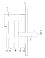
- FIG. 1 there is depicted a schematic view of a basic structure of a conventional OLED.
- the structure of the OLED comprises a substrate 11, an anode 12, a hole transporting layer (HTL) 13, an emission layer (EML) 14, an electron transporting layer (ETL) 15 and a cathode 16.
- HTL hole transporting layer
- EML emission layer
- ETL electron transporting layer
- cathode 16 Organic materials such as the hole transporting layer 13, the emission layer 14, an electron transporting layer 15 are sandwiched between the anode 12 and the cathode 16 to form a sandwich structure.
- the luminous principle of an OLED is that electrons and holes are driven to recombine in the organic materials to excite light emission.
- the luminescent materials will age and degrade with the light emission time.
- the higher the luminous intensity per unit time is, the faster the luminescent materials age and degrade, referred as to differential aging.
- an OLED display tends to display images of a specific color for a long time, it is easy for the OLEDs of the specific color in the display to degrade faster. As a result, the display function of the entire OLED display will be lost or seriously influenced. Therefore, how to effectively prolong the service life of an OLED display is a problem to be urgently solved.
- an object of the present invention is to provide an organic light emitting diode display, a driving method therefor and a pixel unit thereof, so as to prolong the service life of the organic light emitting diode displays.
- an organic light emitting diode display apparatus comprising a pixel array, a signal processing unit, a scan driving unit, a data driving unit and a light emission control unit.
- the pixel array comprises a plurality of pixel units each having an organic light emitting diode, and the plurality of pixel units are divided into a plurality of pixel groups.
- the signal processing unit receives an image and generates a plurality of data signals respectively corresponding to the plurality of pixel units in accordance with the image, and determines a plurality of light emission parameters respectively corresponding to the plurality of pixel groups.
- the scan driving unit generates a plurality of scanning signals in accordance with the plurality of light emission parameters and a frame interval and drives the pixel array in accordance with the plurality of scanning signals.
- the data driving unit drives the plurality of pixel units in accordance with the plurality of data signals.
- the light emission control unit generates a plurality of control signals in accordance with the plurality of light emission parameters to control the respective light emission time of the plurality of pixel groups within the frame interval.
- the plurality of pixel groups display different colors, respectively.
- the plurality of scanning signals correspond to the plurality of pixel columns or the plurality of pixel rows of the pixel array, respectively.
- Each scanning signal includes a plurality of pulses, and the frame interval is between two adjacent pulses.
- Each light emission parameter is a ratio value of a light emission interval or a non-light emission interval of the pixel unit within the frame interval.
- the signal processing unit analyzes a gray scale distribution of the image corresponding to the plurality of pixel groups, and determines light emission parameters corresponding to the plurality of pixel groups in accordance with the gray scale distribution.
- a driving method for an organic light emitting diode display is further provided.
- a pixel unit of the organic light emitting diode display has an organic light emitting diode and a drive circuit.
- the drive circuit is connected to the organic light emitting diode.
- the driving method comprises the following steps of: receiving a data signal and a scanning signal including a frame interval by the drive circuit; generating within the frame interval a current corresponding to the data signal and flowing through the organic light emitting diode in accordance with the scanning signal by the drive circuit; receiving a control signal which defines a first interval and a second interval from the frame interval; controlling the current in accordance with the control signal so that the luminous intensity of the organic light emitting diode in the second interval being lower than the luminous intensity of the organic light emitting diode in the first interval.
- the driving method further comprises analyzing an image received by the organic light emitting diode display, and determining a ratio value of the first interval or the second interval in accordance with the analytical result.
- the pixel unit of the same pixel groups corresponds to the same ratio value of the first interval or the second interval.
- the scanning signal includes a plurality of pulses, and the frame interval is between two adjacent pulses.
- the second interval corresponding to the plurality of pixel rows or the plurality of pixel columns of the pixel array is synchronous.
- a pixel unit comprising an organic light emitting diode, a switch and a drive circuit.
- the drive circuit is coupled to the organic light emitting diode and the switch, and receives a scanning signal including a frame interval and a data signal.
- the drive circuit generates within the frame interval a current corresponding to the data signal and flowing to the organic light emitting diode.
- the switch controls the current flowing toward the organic light emitting diode only in some intervals of the light emission interval.
- the drive circuit comprises a first transistor, a second transistor and a capacitor.
- the source of the first transistor is connected to a data line for receiving the data signal.
- the gate of the first transistor is connected to a scanning line for receiving the scanning signal.
- the source of the second transistor is connected to the anode of the organic light emitting diode.
- the gate of the second transistor is connected to the drain of the first transistor. Both ends of the capacitor are respectively connected to the gate and the drain of the second transistor. Both ends of the switch are connected to the drain of the second transistor and a first voltage source.
- the drive circuit comprises a first transistor, a second transistor and a capacitor.
- the source of the first transistor is connected to a data line for receiving the data signal.
- the gate of the first transistor is connected to a scanning line for receiving the scanning signal.
- the source of the second transistor is connected to the anode of the organic light emitting diode.
- the gate of the second transistor is connected to the drain of the first transistor.
- the drain of the second transistor is connected to a first voltage source. Both ends of the capacitor are respectively connected to the gate of the second transistor and the first voltage source. Both ends of the switch are connected to the source of the second transistor and a second voltage source.
- the drive circuit further comprises a current duplication circuit for duplicating a current flowing through the data line.
- the organic light emitting diode display, the driving method therefor and the pixel unit thereof may have the following advantages: the organic light emitting diode display, the driving method therefor and the pixel unit thereof can determine the ratio of shortened light emission intervals of OLED pixel groups of a specific color based on the color distribution of an image, thereby effectively prolonging the life of the OLEDs of a specific color.
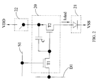
- the pixel driving circuit comprises a drive circuit 20, an organic light emitting diode (OLED) 21 and a switch 22.
- the drive circuit 20 comprises a transistor T1, a transistor T2 and a capacitor C.
- the source of the transistor T1 is connected to a data line D1 for receiving a data signal DATA.
- the gate of the transistor T1 is connected to a scanning line S1 for receiving a scanning signal SCAN.
- the source of the transistor T2 is connected to the anode of the OLED 21.
- the drain of the transistor T2 is connected to a voltage source VDD.
- the gate of the transistor T2 is connected to the drain of the transistor T1.
- One end of the capacitor C is connected to the gate of the transistor T2, and the other end of the capacitor is connected to the switch and the voltage source VDD.
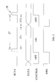
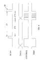
- FIG. 3 there is illustrated a signal timing sequence diagram of a pixel driving circuit of an organic light emitting diode according to the present invention.
- the scanning signal S1 has multiple pulses 28, and two adjacent pulses 28 define a frame interval 27.
- the gate of the transistor T1 receives the pulse signal 28, the voltage at the gate of the transistor T1 is shifted from a low potential to a high potential and the transistor T1 is turned on to provide a closed path between the source and the drain of the transistor T1 so that one end of the capacitor C can receive the data signal DATA for being charged.
- the transistor T1 When the voltage at the gate of the transistor T1 is shifted from a high potential to a low potential, the transistor T1 is turned off to provide an open path between the source and the drain of the transistor T1.
- the voltage between both ends of the capacitor C can be used for controlling the magnitude of a current I oled flowing from the source of the transistor T2 to the OLED 21.
- the luminous intensity of the OLED 21 is associated with the magnitude of the input current. As a result, the aforementioned procedure can control the OLED 21 and enable the luminous intensity of the OLED 21 to correspond to the data signal DATA.
- a plurality of the above-described pixel units are combined to form a pixel array which can display an image.
- the OLED 21 emits light continuously within the frame interval 27.
- the OLED 21 can be controlled to emit light only during some time period in the frame interval 27.
- the switch 22 is controlled by the control signal CONTROL illustrated in FIG. 3 .
- the switch 22 When the control signal CONTROL is at a high potential, the switch 22 is turned on and the voltage source VDD can supply a current I oled to the OLED 21; on the contrary, when the control signal CONTROL is at a low potential, the switch 22 is turned off and the voltage source VDD cannot supply a current I oled to the OLED 21 so that the OLED 21 stops emitting light. Hence, the OLED 21 emits light during the interval 271 within the frame interval 27 and stops emitting light during the interval 272. By this way, the light emission time of the OLED within the frame interval can be effectively controlled without changing the original structure of the pixel unit.
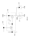
- FIG. 4 there is illustrated a circuit diagram of a second embodiment of a pixel driving circuit of an organic light emitting diode according to the present invention.
- the difference between the second embodiment and the first embodiment is that the switch 32 is connected to the anode of the OLED 21 but not disposed between the voltage source VDD and the transistor T2.
- the switch 32 is controlled by the control signal CONTROL illustrated in FIG. 5 .
- the control signal CONTROL is at a high potential
- the switch 32 is turned on to form a low resistance path which is connected in parallel with the OLED, so that the circuit flows toward this path but toward the OLED 21.
- the voltage source VDD cannot supply a current I oled to the OLED 21, and the OLED 21 stops emitting light.
- a parallel connection with a new path is provided to prevent the I oled from flowing toward the OLED; however, even though the display designer uses this method to decrease the current flowing toward the OLED but not to cause the current to be zero so that the luminous intensity of the OLED during the interval 272 is reduced, this method is included within the protection scope of the present invention; alternatively, if a successive pulse is used as the control signal CONTROL during the interval 272 to adjust the luminous intensity of the OLED during the interval 272, as illustrated in FIG. 6 , so that the luminous intensity of the OLED within the frame interval can be reduced without changing the original structure of the pixel unit, this method is also included within the protection scope of the present invention.
- the control signal illustrated in FIG. 6 can also be applied to the first embodiment.
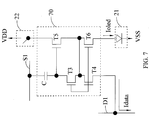
- the drive circuit 70 further comprises a current duplication circuit.
- the current duplication circuit is comprised of transistors T3, T4, T5 and T6 for duplicating a current I data flowing through the data line D 1.
- I oled is equal to I data .
- the switch 22 is connected between the voltage source VDD and the drive circuit 70.
- the operation principle is the same as in the first embodiment and will be explained in no more detail.
- the switch 22 is connected to the anode of the OLED 21 and the voltage source VDD.
- the operation principle is the same as in the second embodiment and will be explained in no more detail.
- the organic light emitting diode display apparatus comprises a pixel array 81, a signal processing unit 82, a scan driving unit 83, a data driving unit 84, a light emission control unit 85 and a voltage source 86.
- the pixel array 81 comprises a plurality of pixel units 811 each having an OLED, and the plurality of pixel units 811 are divided into a plurality of pixel groups.
- the plurality of pixel groups are pixel groups emitting light of different colors.
- the plurality of pixel groups are preferably arranged in columns or rows.
- the pixel array 81 comprises red pixel groups 812, green pixel groups 813 and blue pixel groups 814, and their pixel units comprise a red OLED, a green OLED and a blue OLED, respectively.
- the pixels emitting in the same color are arranged in the same row.
- a plurality of pixel rows emitting red light form red pixel groups 812
- a plurality of pixel rows emitting green light form green pixel groups 813.
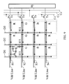
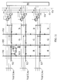
- FIG. 9 depicted is a pixel array 81 formed by a plurality of circuits of the first embodiment of the pixel unit illustrated in FIG. 2 .
- the integrated switch of the pixel units 811 in the same row is implemented by a transistor T R , T B or T G with no effect on its performance.
- the gates of the transistors T R , T B and T G are respectively connected to control lines C R , C B and C G for receiving corresponding control signals 851.
- a control signal 851 at a high potential or a low potential determines whether or not the current outputted from the voltage source 86 flows toward the pixel units 811.
- the signal processing unit 82 receives an image 821 and generates a plurality of data signals 822 respectively corresponding to the plurality of pixel units 811 in accordance with the image 821. In this embodiment, the signal processing unit 82 generates red data signals, green data signals and blue data signals of the image 821. The signal processing unit 82 determines a plurality of light emission parameters 823 respectively corresponding to the plurality of pixel groups 812-814. The scan driving unit 83 generates a plurality of scanning signals 831 in accordance with the plurality of light emission parameters 823 and a frame interval 87 and drives the pixel array 81 in accordance with the plurality of scanning signals 831. The data driving unit 84 drives the plurality of pixel units 811 in accordance with the plurality of data signals 822.
- Each scanning signal 831 includes a plurality of pulses, and two adjacent pulses define the frame interval 87.
- the pixel units 811 in the same row are connected to the same scanning line for receiving the scanning signals 831 and, for example, the pixel units 811 in rows 1 to 4 of the figure are connected to the scanning lines S1-S4, respectively; the pixel units 811 in the same column are connected to the same data line and, for example, the pixel units 811 in columns 1 to 3 of the figure are connected to the data lines D1-D3, respectively.
- the pixel unit 811 When pulses appear in the scanning signal 831, i.e., shifted from a low potential to a high potential, the pixel unit 811 is in a state capable of receiving data signals and the data signals 822 on the data lines D1-D3 can be stored in the pixel units 811.
- the pulses of the plurality of scanning signals 831 are asynchronous with each other and can sequentially activate the pixel units 811 in different rows.
- the data driving unit 84 changes the data signals with pulse variations in the scanning signals 831. Hence, different data can be stored in the plurality of pixel units 811 within the pixel array 81.
- the light emission control unit 85 generates a plurality of control signals 851 in accordance with the plurality of light emission parameters 823 to control the respective light emission time of the plurality of pixel groups within the frame interval 87.
- the control signal 851 on the control line C R is of a high potential
- the transistor T R is turned on and the pixel units within the red pixel groups can receive a current I OLED outputted from the voltage source VDD; on the contrary, when the control signal 851 on the control line C R is of a high potential, the transistor T R is turned off and the pixel units within the red pixel groups cannot receive a current I OLED outputted from the voltage source VDD so that the red OLED does not emit light.
- the light emission parameter 823 is a ratio value of a light emission interval or a non-light emission interval within the frame interval 87, or time length of a light emission interval within the frame interval 87.
- the signal processing unit 82 analyzes a gray scale distribution of the image 821 corresponding to the pixel groups 812-814 and determines light emission parameters 823 corresponding to the pixel groups 812-814 in accordance with the gray scale distribution.
- the scan driving unit 83 can adjust the positions of pulses in the scanning signal 831 in accordance with the light emission parameters 823.
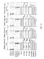
- FIG. 10 there is depicted a signal timing sequence diagram of an embodiment of an organic light emitting diode display apparatus according to the present invention.
- 831(1), 831(2) to 831(n) are the scanning signals 831 respectively used in row 1, rows 2 to n.
- 85 1 (R), 85 1 (G) and 85 1 (B) are control signals respectively used in red, green and blue pixel groups.
- the time that the control signal 851(R) is at high potential is 85% of the corresponding frame interval (light emission interval), and the time that the control signal 851 (R) is at low potential is 15% of the corresponding frame interval (non-light emission interval) within the corresponding frame interval;
- the time that the control signal 851(G) is at high potential is 80% of the corresponding frame interval (light emission interval), and the time that the control signal 851(G) is at low potential is 20% of the corresponding frame interval (non-light emission interval) within the corresponding frame interval;
- the time that the control signal 851(B) is at high potential is 60% of the corresponding frame interval (light emission interval), and the time that the control signal 85 1 (B) is at low potential is 40% of the corresponding frame interval (non-light emission interval) within the corresponding frame interval.
- the scan driving unit 83 can shorten pulse intervals between the plurality of scanning signals 831 in accordance with the signal features of the above-mentioned plurality of control signals 851 so that the pulses of the scanning signals 831 can appear in the light emission interval.
- the second interval corresponding to the plurality of pixel rows of the pixel array is synchronous.
- the same method is used so that the second interval corresponding to the plurality of pixel columns of the pixel array is synchronous.
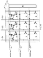
- FIG. 11 there is depicted a schematic circuit diagram of a second embodiment of an organic light emitting diode display apparatus according to the present invention.
- the difference between the second embodiment and the first embodiment is that the pixel units 811 of the same color are disposed in the same column.
- the operation principle is the same as in the first embodiment and will be explained in no more detail.
- FIG. 12 there is depicted a schematic circuit diagram of a third embodiment of an organic light emitting diode display apparatus according to the present invention.
- the difference between the third embodiment and the foregoing two embodiments is that the structures of the pixel units are different.
- the circuit illustrated in FIG. 12 is formed by the pixel units illustrated in FIG. 4 .
- the operation principle has been described above and will be explained in no more detail.
- FIG. 13 there is depicted a signal timing sequence diagram of another embodiment of an organic light emitting diode display apparatus according to the present invention.
- the difference between this timing sequence diagram and the timing sequence diagram of FIG. 10 is that the control signal 851(B) has a plurality of pulses in the non-light emission interval so as to adjust the blue light emission effect of the display apparatus.
- the light emission parameters of each pixel group can be determined after the signal processing unit 82 analyzes the content of an image. Since the purpose of shortening the light emission time of the OLED 21 within the frame interval is to prevent the OLED 21 of a specific color from fast degradation due to excessive light emission, the signal processing unit 82 can analyze a gray scale distribution of different colors in the image 821. When the amount of one color used exceeds a threshold value, the signal processing unit 82 will set a ratio value of a light emission interval or a non-light emission interval within the frame interval 87. The ratio value is used as the light emission parameter 823.
- the scan driving unit 83 and the data driving unit 84 make a corresponding adjustment in accordance with the light emission parameter 823. Referring to FIG.
- gray level histograms for the red, green and blue colors of an image.
- the number of green pixels in the image with a gray value greater than 128 exceeds 50%
- the number of blue pixels with a gray value greater than 128 exceeds 50%.
- the signal processing unit 82 sets the light emission parameters 87 corresponding to the green pixel groups and the blue pixel groups to activate the function of shortening the light emission time of the OLEDs, so that the control signals 85 1 (G) and 85 1 (B) have 20% and 40% non-light emission intervals within the frame interval, as illustrated in FIG. 10 . Since the service life of a current blue OLED is shorter than that of a red OLED or a green OLED, the control signal 85 1 (B) has a longer non-light emission interval.
- the signal processing unit 82 can analyze the image content to determine the respective ratios of the red, green and blue colors of the image content, and determine whether or not to activate the function in accordance with a query table of the corresponding relationship between recorded image contents and set modes, as set forth in Table I. If the user sets the OLED display apparatus to the persistent mode, it means that the user hopes to prolong the service life of the display.
- Table I if the ratio of the red content of an image exceeds 60%, or the ratio of the green content exceeds 30%, or the ratio of the blue content exceeds 10%, the above-mentioned function of shortening the light emission time of the OLEDs is activated. After the activation is determined, the light emission parameters can be determined in accordance with the gray scale distribution of each color. Since the service life of a current blue OLED is shortest, the activation values for the blue color in Table I is lowest. Table I set mode ratios of R/G/B red green blue persistent mode >60% or >30% or >10% balanced mode >30% or >30% or >30% energy-saving mode >10% or >10% or >10%
- the signal processing unit 82 can compensate for the image 821 in a manner to appropriately increase the brightness of specific colors in the image, for example, to adjust the blue gamma curve or the green gamma curve of the image.
- a pixel unit of the organic light emitting diode display has an organic light emitting diode and a drive circuit.
- the drive circuit is connected to the organic light emitting diode.
- the drive circuit receives a data signal and a scanning signal including a frame interval in step A1.
- the drive circuit generates within the frame interval a current corresponding to the data signal and flowing through the organic light emitting diode in accordance with the scanning signal.
- a control signal is received, which defines a first interval and a second interval from the frame interval.
- the current is controlled in accordance with the control signal so that the luminous intensity of the organic light emitting diode in the second interval is lower than the luminous intensity of the organic light emitting diode in the first interval.
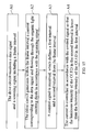
- step B1 an image is received.
- step B2 gray scale distributions of the RGB colors of the image are analyzed and it is determined whether or not to activate the mechanism of shortening the light emission time. If no, step B31 is performed. If yes, step B4 is performed.
- step B31 a plurality of scanning signals are generated, and a plurality of data signals are generated in accordance with the image.
- step B32 a plurality of pixel units within a pixel array are driven in accordance with the scanning signals and the data signals so as to emit light and display the image.
- step B4 light emission parameters of red, green and blue pixel groups, such as the ratio of the light emission interval or the ratio of the non-light emission interval within the frame interval, are determined.
- step B5 it is determined whether or not to compensate for the image in accordance with the gray scale distributions of the RGB colors. If no, step B6 is performed. If yes, a query table of the RGB-compensation values is read or a color conversion procedure is performed to convert colors of the image in step B51. Step B6 is performed after the conversion.
- step B6 a plurality of scanning signals and control signals are generated in accordance with the light emission parameters and the frame interval, and a plurality of data signals are generated in accordance with the original image or the converted image.
- step B7 a plurality of pixel units within a pixel array are driven in accordance with the scanning signals and the data signals so as to emit light.
- step B8 it is controlled whether or not the OLEDs within the pixel units emit light within the frame interval in accordance with the control signals.
- the pixel units of the display are arranged in an array. If the image is displayed only in a specific region of the display, this may result in serious consumption of OLEDs of a specific color. It is possible to perform the above-described action of shortening the light emission time of the pixel units corresponding to a specific color within the specific region via the above-described mechanism.
- the operation principle is similar to the embodiments described above, and will be explained in no more detail.
Landscapes
- Engineering & Computer Science (AREA)
- Physics & Mathematics (AREA)
- Computer Hardware Design (AREA)
- General Physics & Mathematics (AREA)
- Theoretical Computer Science (AREA)
- Electroluminescent Light Sources (AREA)
- Control Of El Displays (AREA)
- Control Of Indicators Other Than Cathode Ray Tubes (AREA)
Applications Claiming Priority (1)
| Application Number | Priority Date | Filing Date | Title |
|---|---|---|---|
| TW098137003A TW201115542A (en) | 2009-10-30 | 2009-10-30 | Organic light emitting diode (OLED) display, driving method thereof, and pixel unit thereof |
Publications (1)
| Publication Number | Publication Date |
|---|---|
| EP2325830A1 true EP2325830A1 (fr) | 2011-05-25 |
Family
ID=43513885
Family Applications (1)
| Application Number | Title | Priority Date | Filing Date |
|---|---|---|---|
| EP10164582A Withdrawn EP2325830A1 (fr) | 2009-10-30 | 2010-06-01 | Affichage à diode électroluminescente organique, son procédé de commande et son unité de pixels |
Country Status (3)
| Country | Link |
|---|---|
| US (1) | US20110102417A1 (fr) |
| EP (1) | EP2325830A1 (fr) |
| TW (1) | TW201115542A (fr) |
Cited By (3)
| Publication number | Priority date | Publication date | Assignee | Title |
|---|---|---|---|---|
| CN104347032A (zh) * | 2014-11-20 | 2015-02-11 | 无锡科思电子科技有限公司 | 一种户外led显示屏驱动电路 |
| CN104347034A (zh) * | 2014-11-20 | 2015-02-11 | 无锡科思电子科技有限公司 | 一种双电源led显示屏驱动电路 |
| CN104347033A (zh) * | 2014-11-20 | 2015-02-11 | 无锡科思电子科技有限公司 | 一种led显示屏驱动电路 |
Families Citing this family (6)
| Publication number | Priority date | Publication date | Assignee | Title |
|---|---|---|---|---|
| EP2106675B1 (fr) * | 2007-01-22 | 2018-11-07 | Philips Intellectual Property & Standards GmbH | Configuration de diodes électroluminescentes organiques |
| KR101992895B1 (ko) * | 2012-12-10 | 2019-09-27 | 엘지디스플레이 주식회사 | 유기 발광 다이오드 표시장치와 그 구동방법 |
| CN104167175B (zh) * | 2014-08-06 | 2016-08-31 | 上海和辉光电有限公司 | 有机发光显示器 |
| KR20160054073A (ko) * | 2014-11-05 | 2016-05-16 | 삼성전자주식회사 | 디스플레이 장치 및 디스플레이 패널 |
| CN104616619B (zh) * | 2014-12-26 | 2017-04-26 | 上海天马有机发光显示技术有限公司 | 阵列基板、显示面板及显示装置 |
| CN106157897B (zh) * | 2016-09-26 | 2018-11-20 | 京东方科技集团股份有限公司 | 一种亮度控制方法、装置、amoled面板和电子设备 |
Citations (3)
| Publication number | Priority date | Publication date | Assignee | Title |
|---|---|---|---|---|
| WO2004049289A1 (fr) * | 2002-11-23 | 2004-06-10 | Koninklijke Philips Electronics N.V. | Controle des couleurs pour dispositif d'affichage electroluminescent a matrice active |
| WO2005008622A1 (fr) * | 2003-07-18 | 2005-01-27 | Koninklijke Philips Electronics N.V. | Dispositif d'affichage a diodes organiques electroluminescentes (oled) |
| WO2009008418A1 (fr) * | 2007-07-11 | 2009-01-15 | Sony Corporation | Unité d'affichage, procédé pour traiter un signal vidéo et programme pour traiter un signal vidéo |
Family Cites Families (3)
| Publication number | Priority date | Publication date | Assignee | Title |
|---|---|---|---|---|
| US7760165B2 (en) * | 2006-09-22 | 2010-07-20 | Global Oled Technology Llc | Control circuit for stacked OLED device |
| JP3909595B2 (ja) * | 2003-04-23 | 2007-04-25 | セイコーエプソン株式会社 | 表示装置、及びその調光方法 |
| KR101006381B1 (ko) * | 2006-02-22 | 2011-01-10 | 삼성전자주식회사 | 발광장치 및 그 제어방법 |
-
2009
- 2009-10-30 TW TW098137003A patent/TW201115542A/zh unknown
-
2010
- 2010-04-29 US US12/770,051 patent/US20110102417A1/en not_active Abandoned
- 2010-06-01 EP EP10164582A patent/EP2325830A1/fr not_active Withdrawn
Patent Citations (3)
| Publication number | Priority date | Publication date | Assignee | Title |
|---|---|---|---|---|
| WO2004049289A1 (fr) * | 2002-11-23 | 2004-06-10 | Koninklijke Philips Electronics N.V. | Controle des couleurs pour dispositif d'affichage electroluminescent a matrice active |
| WO2005008622A1 (fr) * | 2003-07-18 | 2005-01-27 | Koninklijke Philips Electronics N.V. | Dispositif d'affichage a diodes organiques electroluminescentes (oled) |
| WO2009008418A1 (fr) * | 2007-07-11 | 2009-01-15 | Sony Corporation | Unité d'affichage, procédé pour traiter un signal vidéo et programme pour traiter un signal vidéo |
Cited By (3)
| Publication number | Priority date | Publication date | Assignee | Title |
|---|---|---|---|---|
| CN104347032A (zh) * | 2014-11-20 | 2015-02-11 | 无锡科思电子科技有限公司 | 一种户外led显示屏驱动电路 |
| CN104347034A (zh) * | 2014-11-20 | 2015-02-11 | 无锡科思电子科技有限公司 | 一种双电源led显示屏驱动电路 |
| CN104347033A (zh) * | 2014-11-20 | 2015-02-11 | 无锡科思电子科技有限公司 | 一种led显示屏驱动电路 |
Also Published As
| Publication number | Publication date |
|---|---|
| US20110102417A1 (en) | 2011-05-05 |
| TW201115542A (en) | 2011-05-01 |
Similar Documents
| Publication | Publication Date | Title |
|---|---|---|
| EP2325830A1 (fr) | Affichage à diode électroluminescente organique, son procédé de commande et son unité de pixels | |
| US7847764B2 (en) | LED device compensation method | |
| CN1322485C (zh) | 产生伽马电压的装置和方法 | |
| US20050269960A1 (en) | Display with current controlled light-emitting device | |
| KR100550680B1 (ko) | 표시장치 및 표시장치의 구동방법 | |
| US20100060554A1 (en) | Display apparatus and method of driving the same | |
| US20030160743A1 (en) | Color organic EL display device | |
| US8330684B2 (en) | Organic light emitting display and its driving method | |
| CN1711479A (zh) | Led矩阵显示器的检查方法和设备 | |
| CN102054428A (zh) | 有机发光二极管显示器、其驱动方法、及其像素单元 | |
| CN111554238A (zh) | 有机发光二极体显示面板亮度补偿方法 | |
| CN1744178A (zh) | 发光显示屏的驱动装置 | |
| JP4260586B2 (ja) | 表示装置の駆動回路及び駆動方法 | |
| JP2010541012A (ja) | 電流駆動型elディスプレイの電源電圧の動的適応 | |
| KR20060034274A (ko) | 듀티 사이클 제어 기능을 구비한 전자발광 디스플레이디바이스 | |
| US20060221014A1 (en) | Organic light emitting display and method of driving the same | |
| CN110534054B (zh) | 显示驱动方法及装置、显示装置、存储介质、芯片 | |
| KR101246642B1 (ko) | 표시 장치 및 이의 구동 방법 | |
| US7463251B2 (en) | Display device having a sparkling effect and method for driving the same | |
| US20060261744A1 (en) | Drive apparatus and drive method for light emitting display panel | |
| JP2003131619A (ja) | 自己発光型表示装置 | |
| KR100624366B1 (ko) | 표시장치 및 그의 동적 감마 적용방법 | |
| WO2010007366A1 (fr) | Tension de mode commun d'équilibrage dans un dispositif d'affichage à commande de courant | |
| US8847944B2 (en) | Matching current source/sink apparatus | |
| JP2007114285A (ja) | 表示装置及びその駆動方法 |
Legal Events
| Date | Code | Title | Description |
|---|---|---|---|
| PUAI | Public reference made under article 153(3) epc to a published international application that has entered the european phase |
Free format text: ORIGINAL CODE: 0009012 |
|
| AK | Designated contracting states |
Kind code of ref document: A1 Designated state(s): AL AT BE BG CH CY CZ DE DK EE ES FI FR GB GR HR HU IE IS IT LI LT LU LV MC MK MT NL NO PL PT RO SE SI SK SM TR |
|
| AX | Request for extension of the european patent |
Extension state: BA ME RS |
|
| STAA | Information on the status of an ep patent application or granted ep patent |
Free format text: STATUS: THE APPLICATION IS DEEMED TO BE WITHDRAWN |
|
| 18D | Application deemed to be withdrawn |
Effective date: 20111126 |