EP2325896A2 - Electrode frontale pour pile solaire permettant de réduire la perte de puissance, et pile solaire comprenant cette électrode - Google Patents
Electrode frontale pour pile solaire permettant de réduire la perte de puissance, et pile solaire comprenant cette électrode Download PDFInfo
- Publication number
- EP2325896A2 EP2325896A2 EP09813231A EP09813231A EP2325896A2 EP 2325896 A2 EP2325896 A2 EP 2325896A2 EP 09813231 A EP09813231 A EP 09813231A EP 09813231 A EP09813231 A EP 09813231A EP 2325896 A2 EP2325896 A2 EP 2325896A2
- Authority
- EP
- European Patent Office
- Prior art keywords
- grid electrodes
- pattern part
- front electrode
- electrodes
- width
- Prior art date
- Legal status (The legal status is an assumption and is not a legal conclusion. Google has not performed a legal analysis and makes no representation as to the accuracy of the status listed.)
- Granted
Links
Images


Classifications
-
- H—ELECTRICITY
- H10—SEMICONDUCTOR DEVICES; ELECTRIC SOLID-STATE DEVICES NOT OTHERWISE PROVIDED FOR
- H10F—INORGANIC SEMICONDUCTOR DEVICES SENSITIVE TO INFRARED RADIATION, LIGHT, ELECTROMAGNETIC RADIATION OF SHORTER WAVELENGTH OR CORPUSCULAR RADIATION
- H10F10/00—Individual photovoltaic cells, e.g. solar cells
-
- H—ELECTRICITY
- H10—SEMICONDUCTOR DEVICES; ELECTRIC SOLID-STATE DEVICES NOT OTHERWISE PROVIDED FOR
- H10F—INORGANIC SEMICONDUCTOR DEVICES SENSITIVE TO INFRARED RADIATION, LIGHT, ELECTROMAGNETIC RADIATION OF SHORTER WAVELENGTH OR CORPUSCULAR RADIATION
- H10F77/00—Constructional details of devices covered by this subclass
- H10F77/20—Electrodes
- H10F77/206—Electrodes for devices having potential barriers
- H10F77/211—Electrodes for devices having potential barriers for photovoltaic cells
- H10F77/215—Geometries of grid contacts
-
- H—ELECTRICITY
- H10—SEMICONDUCTOR DEVICES; ELECTRIC SOLID-STATE DEVICES NOT OTHERWISE PROVIDED FOR
- H10F—INORGANIC SEMICONDUCTOR DEVICES SENSITIVE TO INFRARED RADIATION, LIGHT, ELECTROMAGNETIC RADIATION OF SHORTER WAVELENGTH OR CORPUSCULAR RADIATION
- H10F77/00—Constructional details of devices covered by this subclass
- H10F77/20—Electrodes
-
- Y—GENERAL TAGGING OF NEW TECHNOLOGICAL DEVELOPMENTS; GENERAL TAGGING OF CROSS-SECTIONAL TECHNOLOGIES SPANNING OVER SEVERAL SECTIONS OF THE IPC; TECHNICAL SUBJECTS COVERED BY FORMER USPC CROSS-REFERENCE ART COLLECTIONS [XRACs] AND DIGESTS
- Y02—TECHNOLOGIES OR APPLICATIONS FOR MITIGATION OR ADAPTATION AGAINST CLIMATE CHANGE
- Y02E—REDUCTION OF GREENHOUSE GAS [GHG] EMISSIONS, RELATED TO ENERGY GENERATION, TRANSMISSION OR DISTRIBUTION
- Y02E10/00—Energy generation through renewable energy sources
- Y02E10/50—Photovoltaic [PV] energy
Definitions
- the present invention relates to a front electrode for solar cells having minimized power loss and a solar cell including the same, and, more particularly, to a front electrode for solar cells, wherein the front electrode is configured in a structure in which a pattern including a plurality of grid electrodes arranged in parallel and at least one current collection electrode intersecting the grid electrodes is formed on a semiconductor substrate, current introduced to the grid electrodes is moved to and collected in the current collection electrode, and the width of each of the grid electrodes is increased toward the current collection electrode.
- Solar cells may be classified into solar thermal cells which generate steam energy necessary to rotate a turbine using solar heat and photovoltaic solar cells which convert photons into electric energy using properties of semiconductors.
- photovoltaic solar cells which absorb light, generating electrons and holes and thereby converting light energy into electric energy.
- FIG. 1 is a view typically illustrating the structure of such a photovoltaic solar cell (hereinafter, simply referred to as a "solar celt").
- the solar cell includes a first conduction type semiconductor layer 22 and a second conduction type semiconductor layer 23, which is opposite to the conduction type of the first conduction type semiconductor layer 22, formed on first conduction type semiconductor layer 22.
- a p/n junction is achieved at the interface between the first conduction type semiconductor layer 22 and the second conduction type semiconductor layer 23.
- a rear electrode 21 is disposed in contact with at least a portion of the first conduction type semiconductor layer 22, and a front electrode 11 is disposed in contact with at least a portion of the second conduction type semiconductor layer 23.
- an anti-reflective film 24 to disturb light reflection may be formed at the top of the second conduction type semiconductor layer 23.
- a p-type silicon substrate is usually used as the first conduction type semiconductor layer 22, and an n-type emitter layer is used as the second conduction type semiconductor layer 23.
- the front electrode 11 is usually formed at the top of the emitter layer 23 using a silver (Ag) pattern
- the rear electrode 21 is usually formed at the bottom of the semiconductor layer 22 using an aluminum (Al) layer.
- the front electrode 11 and the rear electrode 21 are generally formed using a screen printing method.
- the front electrode generally includes two current collection electrodes (also referred to as 'bus bars') having a large width and grid electrodes (also referred to as 'fingers') having a small width of approximately 150 ⁇ m.
- the performance of the solar cell which directly converts light energy into electric energy is expressed by a ratio of electric energy output from the solar cell to solar energy incident on the solar cell. This ratio indicates a performance index of the solar cell and is generally referred to as "energy conversion efficiency,” or simply “conversion efficiency.”
- conversion efficiency is limited by a material constituting a solar cell and is controlled according to matching of a spectrum of solar light energy and a sensitivity spectrum of a solar cell. For example, a single crystal silicon solar cell has a conversion efficiency of approximately 30 to 35 %, a noncrystalline silicon solar cell has a conversion efficiency of approximately 25 %, and a compound semiconductor solar cell has a conversion efficiency of approximately 20 to 40 %. On the present laboratory level, however, a solar cell has a conversion efficiency of approximately 25 %.
- Loss may include loss caused by light reflected from a surface, loss caused by recombination of a carrier at the surface or an electrode interface, loss caused by recombination of the carrier in a solar cell, and loss caused by interval resistance of the solar cell.
- Power loss caused by electrodes may include resistance loss caused by movement of light current at an n-type semiconductor layer, loss caused by contact resistance between the n-type semiconductor layer and grid electrodes, resistance loss caused by photoelectric current flowing in the grid electrodes, and loss caused by an area covered by the grid electrodes.
- the present invention has been made to solve the above problems, and other technical problems that have yet to be resolved.
- a front electrode for solar cells wherein the front electrode is configured in a structure in which a pattern including a plurality of grid electrodes arranged in parallel and at least one current collection electrode intersecting the grid electrodes is formed on a semiconductor substrate, current introduced to the grid electrodes is moved to and collected in the current collection electrode, and the width of each of the grid electrodes is increased toward the current collection electrode.
- conventional grid electrodes have a very large and uniform width of approximately 120 to 150 ⁇ m with the result that the area of regions (shadows) covered by the grid electrodes is large, resulting in high electrode loss.
- the inventors of the present application have considered a relationship between a loss of the grid electrodes and the size of the grid electrodes and the current collection electrode so as to develop a structure that is capable of minimizing a loss caused by the grid electrodes.
- electrode loss includes ⁇ a loss (loss I) caused when current flows in the n-type semiconductor layer, ⁇ loss (loss II) caused when the current flows from the n-type semiconductor layer to the grid electrodes, ⁇ loss (loss III) caused when the current flows in the grid electrodes, and ⁇ loss (loss IV) caused by an area covered by the grid electrodes.
- the loss may be calculated as follows with reference to FIG. 2 .
- Loss I ⁇ b 2 ⁇ n - 2 ⁇ x
- Loss II ⁇ b x ⁇ c 1 / 2 ⁇ n - 1 ⁇ x ⁇ c 1 / 2
- Loss III ⁇ L a 2 ⁇ x b / t a ⁇ x W a ⁇ L a 2 ⁇ x n - 1 ⁇ x W a - 2
- Loss IV ⁇ W a x n
- b indicates the intervals of the grid electrodes
- n indicates the number of the grid electrodes
- ⁇ c indicates contact specific resistance between the grid electrodes and the n-type semiconductor layer
- L a indicates the length of the front electrode
- t a indicates the thickness (height) of the grid electrodes
- W a indicates the width of the grid electrodes.
- the width of the grid electrodes may be small.
- the length of the grid electrodes is equal to or greater than a predetermined length, however, it is preferable for the width of the grid electrodes to be small in consideration of resistance.
- the grid electrodes are configured to have a structure in which the width of the grid electrodes is increased toward the current collection electrode at which the amount of current increases. Also, it is preferable for the grid electrodes to be at right angles to the current collection electrode in consideration of efficiency per unit area.
- the width of each of the grid electrodes may be increased so that the width of each of the grid electrodes at one end thereof adjacent to the current collection electrode is preferably 50 to 500 %, more preferably 200 to 500 %, greater than the width of each of the grid electrodes at the other end thereof distant from the current collection electrode.
- the width of each of the grid electrodes may be variously increased toward the current collection electrode.
- the width of each of the grid electrodes may be continuously increased in inverse proportion to the distance from the current collection electrode.
- each of the grid electrodes may be continuously increased, for example, in a straight structure having the shape of a linear function or in a curved structure having the shape of a quadratic function.
- each of the grid electrodes may be discontinuously increased in inverse proportion to the distance from the current collection electrode.
- each of the grid electrodes may be discontinuously increased, for example, in a stair type structure or in a basin type structure.
- the pattern may include a first pattern part at which the width of each of the grid electrodes is 150 ⁇ m or less and a second pattern part at which the width of each of the grid electrodes is less than that of each of the grid electrodes at the first pattern part.
- the front electrode is configured to have such a combination type structure having a first pattern part at which the width of each of the grid electrodes is relatively large and a second pattern part at which the width of each of the grid electrodes is relatively small as described above, it is possible to effectively deal with the amount of current cumulatively increasing based on the length of the grid electrodes, thereby minimizing loss due to the increase in current resistance.
- the first pattern part at the grid electrodes located at the current collection electrode at which the amount of current increases so that the first pattern part has a predetermined length.
- the grid electrodes it is preferable for the grid electrodes to be at right angles to the current collection electrode in consideration of efficiency per unit area.
- the width of the current collection electrode is approximately 1.5 to 3 mm, and two current collection electrodes are provided so that the current collection electrodes are spaced apart from each other by a predetermined distance.
- the second pattern part may be configured to have a structure in which two or more grid electrodes are joined to each other.
- the grid electrodes, having the relatively small width, of the second pattern part are connected to the grid electrodes of the first pattern part while the grid electrodes of the second pattern part are joined to each other, and therefore, it is possible to lower power loss caused during movement of current between the first pattern part and the second pattern part to a negligible level.
- the structure in which the grid electrodes are joined to each other at the second pattern part may be a dendrite structure in which end connection is achieved between the grid electrodes of the first pattern part and the grid electrodes of the second pattern part.
- the electrodes to interconnect the grid electrodes of the first pattern part and the grid electrodes of the second pattern part will be referred to as dendrite electrodes.
- the width of the grid electrodes at the first pattern part and the second pattern part is adjusted so that the increase of resistance due to current accumulation is minimized while shadow loss due to the grid electrodes is minimized.
- the second pattern part is a portion to which current is introduced, and therefore, current accumulation is low.
- the grid electrodes it is preferable for the grid electrodes to have a relatively small width. If the width of the grid electrodes is excessively small, however, it is difficult to form the grid electrodes and, in addition, resistance increases.
- the first pattern part is a portion from which current is discharged to the current collection electrode (also functioning as a current introduction portion according to circumstances).
- the grid electrodes In order to minimize the increase of resistance due to current accumulation, therefore, it is preferable for the grid electrodes to have a relatively large width. If the width of the grid electrodes is excessively large, however, shadow loss is caused and materials are wasted.
- the width of each of the dendrite electrodes may be one to two times, preferably 1 to 1.5 times, that of each of the grid electrodes of the second pattern part.
- each of the grid electrodes of the first pattern part may be 1.1 to 15 times, preferably 3 to 5 times, that of each of the grid electrodes of the second pattern part within a range greater than that of each of the dendrite electrodes.
- the width of each of the grid electrodes of the second pattern part may be 10 to 60 ⁇ m, preferably 10 to 40 ⁇ m, and the width of each of the grid electrodes of the first pattern part may be 50 to 150 ⁇ m, preferably 60 to 100 ⁇ m, within a range greater than that of each of the grid electrodes of the second pattern part.
- the width of each of the dendrite electrodes may be equal to that of each of the grid electrodes of the second pattern part or 10 to 60 ⁇ m, preferably 10 to 50 ⁇ m, within a range greater than that of each of the grid electrodes of the second pattern part.
- the width of each of the grid electrodes at the second part is less than that of each of the conventional grid electrodes, shadow loss is not increased even when the intervals of the grid electrodes, which are approximately 2.5 to 3 mm in the conventional art, are reduced. Furthermore, the movement distance of current is decreased, thereby further improving efficiency.
- the grid electrodes of the first pattern part have a greater width than those of the second pattern part, on the other hand, it is preferable to set the intervals of the grid electrodes at the first pattern part so that the intervals of the grid electrodes at the first pattern part are not much less than those of the grid electrodes at the second pattern part in order to minimize shadow loss.
- the intervals of the grid electrodes of the first pattern part may be 0.7 to 6 times, preferably 1 to 3 times, those of the grid electrodes of the second pattern part.
- the intervals of the grid electrodes of the second pattern part may be 0.5 to 2 mm, and the intervals of the grid electrodes of the first pattern part may be equal to those of grid electrodes of the second pattern part or 1.5 to 3 mm within a range greater than those of the grid electrodes of the second pattern part.
- the dendrite electrodes are preferably inclined at an angle of 30 to 70 degrees to the longitudinal direction of the grid electrodes.
- the length of the second pattern part is greater than 70 % the total length of the grid electrodes or the length of the first pattern part is less than 30 % the total length of the grid electrodes, current resistance is excessively increased.
- the length of the second pattern part is less than 10 % the total length of the grid electrodes or the length of the first pattern part is greater than 90 % the total length of the grid electrodes, shadow loss is increased.
- the length of each of the grid electrodes of the second pattern part is preferably 10 to 70 % the total length of each of the grid electrodes. Also, it is preferable for the length of each of the grid electrodes of the first pattern part to be 30 to 90 % the total length of each of the grid electrodes. If the length of each of the dendrite electrodes is large, the length of each of the grid electrodes is excessively increased. Consequently, the length of each of the dendrite electrodes is preferably 0 to 10 % the total length of each of the grid electrodes.
- the semiconductor substrate may include an n-type semiconductor layer formed of crystalline silicon. According to circumstances, various kinds of layers may be added to the semiconductor substrate. For example, an anti-reflective film may be applied to the top of a dopant layer of an N+ semiconductor layer. Silicon nitride or silicon oxide may be used as the anti-reflective film.
- the resistance of the n-type semiconductor layer may be 50 ⁇ or more, preferably 100 ⁇ or more.
- a solar cell including the front electrode as described above.
- the structure of the grid electrodes is optimized with the result that the solar cell has an electrode loss of 1.3 mW/cm 2 or less. Consequently, the solar cell according to the present invention has an advantage in that conversion efficiency is very high.
- the solar cell may be formed of a bulk type material.
- the solar cell is formed of crystalline silicon in consideration of efficiency.
- the structure and manufacturing method of the solar cell are well known in the art to which the present invention pertains, and therefore, a detailed description thereof will not be given.
- a method of manufacturing a front electrode for solar cells is provided.
- Conventional front electrodes are manufactured using a screen printing method.
- ink is pushed between screen masks to print the front electrodes.
- the screen printing method has a precision of approximately 100 ⁇ m, and therefore, it is not possible to achieve a pattern of less than 100 ⁇ m using the screen printing method, with the result that electrode loss is high.
- ink is pushed through squeezing with the result that the screen printing method is not suitable for a continuous process.
- the manufacturing method according to the present invention upon forming a pattern including a plurality of grid electrodes arranged in parallel and a current collection electrode intersecting the grid electrodes on a semiconductor substrate, includes printing paste on a semiconductor substrate using a gravure printing method or an offset printing method so that the grid electrodes have a width of 100 ⁇ m or less and (b) heating and/or pressurizing the paste to harden the paste.
- the front electrode is formed using the gravure printing method or the offset printing method as described above, it is possible to easily form a micrometer scale pattern and to form the pattern through a continuous process, thereby greatly improving process efficiency.
- the offset printing method may include (i) preparing a printing substrate having grooves formed in a predetermined pattern corresponding to that of the front electrode, (ii) filling the grooves formed at the printing substrate with paste for electrode formation, (iii) rotating a printing roll on the printing substrate to transfer the paste placed in the grooves to the printing roll, and (iv) rotating the printing roll on a semiconductor substrate to transfer the paste from the printing roll to the semiconductor substrate.
- the offset printing method has a patterning precision of approximately 10 to 20 ⁇ m, and the thickness of a pattern formed using the offset printing method is merely several ⁇ m. Consequently, the offset printing method has an advantage of forming a pattern having a sub-micrometer size. Also, in the offset printing method, the paste is transferred to the substrate using the printing roll. Consequently, it is possible to form a pattern through a single transfer process using a printing roll having a size corresponding to the area of the substrate even when the area of the substrate is large.
- the gravure printing method may include (i) preparing a blanket cylinder having grooves formed in a predetermined pattern corresponding to that of the front electrode, (ii) filling the grooves formed at the blanket cylinder with paste for electrode formation, and (iii) rotating the blanket cylinder on a semiconductor substrate to transfer the paste from the blanket cylinder to the semiconductor substrate.
- the gravure printing method has an advantage of suitably forming a micrometer scale pattern and of simultaneously patterning a large area in the same manner as the offset printing method.
- the paste contains a material used to form the grid electrodes and the current collection electrode constituting the front electrode.
- the paste contains silver (Ag) powder.
- the step of curing the paste may include preliminarily drying the paste at a temperature of 150 to 200 °C, removing a binder at a temperature of 400 to 5200 °C, and sintering the paste at a temperature of 750 to 850 °C.
- the total time necessary to cure the paste may be 5 to 10 minutes.
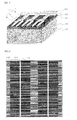
- FIGS. 3 and 4 are partial plan views typically illustrating front electrodes according to embodiments of the present invention.
- each grid electrode 110 includes a first pattern part A adjacent to a current collection electrode 120, a second pattern part B distant from the current collection electrode 120, and a dendrite electrode C located between the first pattern part A and the second pattern part B.
- the first pattern part A At the first pattern part A, grid electrodes each having a relatively large width are arranged at large intervals.
- grid electrodes each having a relatively small width are arranged at small intervals.
- the amount of current introduced is maximized by the second pattern part B, whereas current resistance and shadow loss are minimized by the first pattern part A.
- every two grid electrodes of the second pattern part are joined to each other via each dendrite electrode C.
- all grid electrodes of the second pattern part are joined to each other via the corresponding dendrite electrodes C.
- the grid electrodes at the first pattern part are arranged at relatively small intervals. In consideration of a shadow loss, therefore, the grid electrodes may have a smaller width than the grid electrodes at the first pattern part of FIG. 3 .
- FIG. 6 is a typical view illustrating a process of manufacturing a front electrode using an offset printing method according to an embodiment of the present invention.
- grooves 301 having a shape corresponding to a pattern of a front electrode to be formed at a semiconductor substrate are formed at a printing substrate 300.
- a method of forming the grooves 301 is not particularly restricted.
- the grooves 301 may be formed using a well-known method, such as photolithography.
- the interiors of the grooves 301 are filled with paste 310 for electrode formation.
- the paste 310 is applied to the surface of the printing substrate 300, and a doctor blade 330 is moved in a state in which the doctor blade 330 is in contact with the printing substrate 300. With the movement of the doctor blade 330, the interiors of the grooves 301 are filled with the paste 310.
- the remaining paste 310 may be removed from the printing substrate 300 by the doctor blade 330.
- the paste 310 placed in the grooves 301 of the printing substrate 300 is transferred to the surface of a printing roll 340, which is rotated in a state in which the printing roll 340 is in contact with the printing substrate 300.
- the printing roll 340 may have the same width as a semiconductor substrate 204 at which a pattern is to be formed. Also, the printing roll 340 may have a circumference equal to the length of the semiconductor substrate 204. Consequently, all of the paste 310 placed in the grooves 301 of the printing substrate 300 is transferred to the circumferential surface of the printing roll 340 by a single rotation of the printing roll 340.
- the printing roll 340 is rotated in a state in which the printing roll 340 is in contact with the surface of the semiconductor substrate 204.
- the paste 310 is transferred from the printing roll 340 to the semiconductor substrate 204.
- the paste transferred to the semiconductor substrate 204 is cured to form a pattern.
- the front electrode is patterned using the offset printing method as described above, it is possible to easily form a micrometer scale pattern.
- the printing substrate 300 and the printing roll 340 are manufactured so as to correspond to the size of the semiconductor substrate 204. Consequently, it is possible to form the pattern through a single transfer process, thereby greatly improving process efficiency.
- FIG. 7 is a partial perspective view typically illustrating a solar cell having the front electrode of FIG. 3 .
- the solar cell include a p-type semiconductor layer 202 and an n-type semiconductor layer 203, which is opposite to the conduction type of the p-type semiconductor layer 202, formed on the p-type semiconductor layer 202.
- a p/n junction is achieved at the interface between the p-type semiconductor layer 202 and the n-type semiconductor layer 203.
- a rear electrode 201 is formed at the bottom of the p-type semiconductor layer 202.
- An anti-reflective film 204 having a honeycomb structure to disturb light reflection is formed at the top of the n-type semiconductor layer 203.
- a front electrode 110 including grid electrodes and a current collection electrode 120 is formed on the anti-reflective film 204 in a state in which the front electrode is in contact with at least a portion of the n-type semiconductor layer 203.
- a p-type silicon substrate is usually used as the p-type semiconductor layer 202, and a phosphorous (P)-doped n-type emitter layer is used as the n-type semiconductor layer 203.
- the front electrode 110 is usually formed of a silver (Ag) pattern
- the rear electrode 210 disposed at the bottom of the p-type semiconductor layer 202 is usually formed of an aluminum (Al) layer.
- the front electrode includes a first pattern part 110A including grid electrodes perpendicularly connected to the current collection electrode 120, which has a large width, each of the grid electrodes having a width of 150 ⁇ m or less, a second pattern part 110B including grid electrodes having a smaller width than the grid electrodes of the first pattern part A, and dendrite electrodes 110C including grid electrodes interconnecting the grid electrodes of the first pattern part 110A and the grid electrodes of the second pattern part 110B.
- the increase in resistance of current, introduced from the n-type semiconductor layer 203 to the second pattern part B, flowing in the grid electrodes 110 is minimized by the first pattern part A.
- the intervals of the grid electrodes at the first pattern part 110A are configured to be large, and the intervals of the grid electrodes at the second pattern part 110B are configured to be small, thereby minimizing power loss.
- FIG. 8 is a plan view typically illustrating a front electrode of a solar cell according to the present invention.
- the front electrode is configured to have a structure in which grid electrodes are arranged between two current collection electrodes 120 so that the grid electrodes are perpendicular to the current collection electrodes 120.
- First pattern parts 110A having a relatively large thickness are connected to the respective current collection electrodes 120 so that the first pattern parts 110A are perpendicular to the current collection electrodes 120.
- second pattern parts 110B are connected to the respective first pattern parts 110A.
- the first pattern parts 110A and the second pattern parts 110B are connected to each other in a middle portion defined between the two current collection electrodes 120.
- Phosphorous (P) was diffused on a crystalline p-type silicon substrate to form an n layer having a resistance of 50 ohm, and an anti-reflective silicon nitride (SiNx) layer was deposited at the front of the n layer.
- Aluminum (Al) paste was screen printed and hardened on the rear of the substrate having the p-n junction as described above to form a rear electrode layer, and an electrode was formed at the front of the n layer in the shape shown in FIG. 3 through an offset printing method using silver (Ag) paste.
- grid electrodes of a first pattern part A were formed to have a length of 2.6 cm
- grid electrodes of a second pattern part B were formed to have a length of 1 cm.
- the grid electrodes of the first pattern part A were formed to have a width of 90 ⁇ m and intervals of 1 mm.
- Dendrite electrodes C were formed to have a length of 0.05 cm.
- a solar cell having a resistance of 50 ohm at the n layer was manufactured using the electrode formed as described above.
- a solar cell having a resistance of 100 ohm at an n layer was manufactured using the same method as in Example 1 except that the grid electrodes of the first pattern part were formed to have a length of 2.4 cm, the grid electrodes of the second pattern part were formed to have a length of 1.2 cm, the grid electrodes of the first pattern part were formed to have a width of 20 ⁇ m and intervals of 0.83 mm, and the dendrite electrodes C were formed to have a length of 0.05 cm.
- Grid electrodes were formed into a shape as shown in FIG. 5 to have a width of 120 ⁇ m and intervals of 2.5 mm, thereby manufacturing a solar cell having a resistance of 50 ohm at an n layer.
- Grid electrodes were formed to have a width of 20 ⁇ m and intervals of 1 mm into a shape as shown in FIG. 5 , thereby manufacturing a solar cell having a resistance of 50 ohm at an n layer.
- Grid electrodes were formed into a shape as shown in FIG. 5 to have a width of 120 ⁇ m and intervals of 2.5 mm, thereby manufacturing a solar cell having a resistance of 100 ohm at an n layer.
- Grid electrodes were formed to have a width of 20 ⁇ m and intervals of 1 mm into a shape as shown in FIG. 5 , thereby manufacturing a solar cell having a resistance of 100 ohm at an n layer.
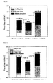
- the n-type loss (loss I) is caused when current flows in the n-type semiconductor layer
- the contact loss (loss II) is caused when the current flows from the n-type semiconductor layer to the grid electrodes
- the finger loss (loss III) is caused when the current flows in the grid electrodes
- the shadow loss (loss IV) is caused by an area covered by the grid electrodes.
- Example 1 was compared with Comparative examples 1 and 2 having an emitter resistance of 50 ohm
- Example 2 was compared with Comparative examples 3 and 4 having an emitter resistance of 50 ohm.
- the grid electrodes were excessively thin and arranged at small intervals, and therefore, the resistance of current flowing in the grid electrodes was increased with the result that loss III was very high, whereas loss III was greatly reduced for the battery of Example 1. Also, it can be seen that, for the battery of Comparative example 1, the grid electrodes had a large width and large intervals, and therefore, shadow loss was very high, whereas the shadow loss was greatly reduced for the battery of Example 1.
- the power loss of the battery of Example 1 was 0.21 % lower than that of battery of Comparative example 1 and 0.79 % lower than that of battery of Comparative example 2.
- the front electrode according to the present invention can be preferably applied to even in a case in which a high-resistance n-type semiconductor layer is used so as to reduce surface recombination velocity of current.
- the front electrode for solar cells according to the present invention is configured to have a structure in which the width of the grid electrodes is increased toward the current collection electrode, thereby minimizing the increase of resistance while minimizing shadow loss and thus reducing power loss. Consequently, it is possible to manufacture a solar cell exhibiting high efficiency.
Landscapes
- Photovoltaic Devices (AREA)
Applications Claiming Priority (2)
| Application Number | Priority Date | Filing Date | Title |
|---|---|---|---|
| KR20080090073 | 2008-09-12 | ||
| PCT/KR2009/005096 WO2010030109A2 (fr) | 2008-09-12 | 2009-09-09 | Electrode frontale pour pile solaire permettant de réduire la perte de puissance, et pile solaire comprenant cette électrode |
Publications (3)
| Publication Number | Publication Date |
|---|---|
| EP2325896A2 true EP2325896A2 (fr) | 2011-05-25 |
| EP2325896A4 EP2325896A4 (fr) | 2017-10-18 |
| EP2325896B1 EP2325896B1 (fr) | 2024-10-30 |
Family
ID=42005618
Family Applications (1)
| Application Number | Title | Priority Date | Filing Date |
|---|---|---|---|
| EP09813231.9A Active EP2325896B1 (fr) | 2008-09-12 | 2009-09-09 | Electrode frontale pour pile solaire permettant de réduire la perte de puissance, et pile solaire comprenant cette électrode |
Country Status (6)
| Country | Link |
|---|---|
| US (1) | US20110247688A1 (fr) |
| EP (1) | EP2325896B1 (fr) |
| JP (1) | JP5497043B2 (fr) |
| KR (2) | KR101089088B1 (fr) |
| CN (1) | CN102171837B (fr) |
| WO (1) | WO2010030109A2 (fr) |
Cited By (5)
| Publication number | Priority date | Publication date | Assignee | Title |
|---|---|---|---|---|
| CN102569528A (zh) * | 2012-02-23 | 2012-07-11 | 常州天合光能有限公司 | 选择性接触的太阳电池前电极的制作方法 |
| CN103718306A (zh) * | 2011-06-14 | 2014-04-09 | 荷兰能源研究中心基金会 | 光伏电池 |
| EP2924740A4 (fr) * | 2012-11-21 | 2016-07-27 | Choshu Industry Co Ltd | Dispositif photovoltaïque |
| EP2595196A4 (fr) * | 2010-06-25 | 2017-04-19 | Kyocera Corporation | Élément de cellule solaire ainsi que procédé de fabrication de celui-ci, et module de cellule solaire |
| WO2017198961A1 (fr) * | 2016-05-20 | 2017-11-23 | S'tile | Assemblage de cellules photovoltaiques |
Families Citing this family (28)
| Publication number | Priority date | Publication date | Assignee | Title |
|---|---|---|---|---|
| US8084293B2 (en) * | 2010-04-06 | 2011-12-27 | Varian Semiconductor Equipment Associates, Inc. | Continuously optimized solar cell metallization design through feed-forward process |
| KR20120062431A (ko) * | 2010-12-06 | 2012-06-14 | 엘지전자 주식회사 | 태양전지 |
| US20120211079A1 (en) * | 2011-02-23 | 2012-08-23 | International Business Machines Corporation | Silicon photovoltaic element and fabrication method |
| KR101115399B1 (ko) * | 2011-03-04 | 2012-02-15 | 한국과학기술원 | 태양전지용 금속 그리드 라인 형성 방법 |
| KR101137380B1 (ko) | 2011-03-07 | 2012-04-20 | 삼성에스디아이 주식회사 | 광전변환소자 및 그 제조방법 |
| US20140102523A1 (en) * | 2011-04-07 | 2014-04-17 | Newsouth Innovations Pty Limited | Hybrid solar cell contact |
| CN102403374A (zh) * | 2011-11-09 | 2012-04-04 | 江西赛维Ldk太阳能高科技有限公司 | 太阳能电池片、太阳能电池串和太阳能电池组件 |
| CN102403373B (zh) * | 2011-11-09 | 2017-05-24 | 江西赛维Ldk太阳能高科技有限公司 | 太阳能电池片、太阳能电池串和太阳能电池组件 |
| TWI643352B (zh) * | 2012-05-30 | 2018-12-01 | 晶元光電股份有限公司 | 光電電池 |
| CN103489930B (zh) * | 2012-06-12 | 2018-02-06 | 晶元光电股份有限公司 | 聚光型光电电池 |
| DE102012219712A1 (de) * | 2012-10-29 | 2014-04-30 | Tridonic Dresden Gmbh & Co. Kg | Leuchtmodul mit optimierter Kontaktierung |
| TWI469363B (zh) * | 2012-10-31 | 2015-01-11 | Topcell Solar Internat Co Ltd | 太陽能電池的正面電極及其製造方法 |
| TWI496302B (zh) * | 2013-01-31 | 2015-08-11 | Motech Ind Inc | 太陽能電池 |
| US20140338718A1 (en) * | 2013-03-12 | 2014-11-20 | Crystal Solar, Inc. | Low shading loss solar module |
| TWI509818B (zh) * | 2013-03-20 | 2015-11-21 | Motech Ind Inc | 太陽能電池、其製造方法及其模組 |
| WO2015029657A1 (fr) | 2013-08-29 | 2015-03-05 | 三洋電機株式会社 | Cellule solaire |
| CN103985772A (zh) * | 2014-04-10 | 2014-08-13 | 晶澳太阳能有限公司 | 一种高性能晶体硅电池的制备方法 |
| US9806206B2 (en) | 2015-04-28 | 2017-10-31 | International Business Machines Corporation | Optimized grid design for concentrator solar cell |
| JP6395941B2 (ja) * | 2015-08-07 | 2018-09-26 | 三菱電機株式会社 | 太陽電池セルおよび太陽電池セルの製造方法 |
| TW201719911A (zh) * | 2015-08-13 | 2017-06-01 | 3M新設資產公司 | 具有在窄前匯流排上之前側匯流排膠帶的光伏電池 |
| DE102015118524B4 (de) * | 2015-10-29 | 2022-01-27 | Infineon Technologies Ag | Halbleiterbauelement mit isoliertem Gate mit sanftem Schaltverhalten und Verfahren zu dessen Herstellung |
| CN105428461B (zh) * | 2015-12-18 | 2017-08-04 | 四川钟顺太阳能开发有限公司 | 中低倍聚光太阳电池的生产工艺以及太阳电池片 |
| KR101894582B1 (ko) * | 2016-11-17 | 2018-10-04 | 엘지전자 주식회사 | 태양 전지 및 이를 포함하는 태양 전지 패널 |
| KR101879374B1 (ko) | 2017-02-22 | 2018-08-17 | 주식회사 탑선 | 태양전지모듈 |
| JP7069158B2 (ja) * | 2017-07-03 | 2022-05-17 | 株式会社カネカ | 太陽電池および太陽電池モジュール |
| TW202112054A (zh) * | 2019-06-03 | 2021-03-16 | 美商索拉利亞股份有限公司 | 低指間距疊瓦太陽能電池 |
| CN110660874A (zh) * | 2019-09-30 | 2020-01-07 | 通威太阳能(合肥)有限公司 | 一种副栅电极及太阳能电池 |
| CN116364788A (zh) * | 2021-12-27 | 2023-06-30 | 隆基绿能科技股份有限公司 | 一种太阳能电池及其电极 |
Family Cites Families (15)
| Publication number | Priority date | Publication date | Assignee | Title |
|---|---|---|---|---|
| JPS629750Y2 (fr) * | 1981-01-12 | 1987-03-06 | ||
| US4590327A (en) * | 1984-09-24 | 1986-05-20 | Energy Conversion Devices, Inc. | Photovoltaic device and method |
| JPH06283736A (ja) * | 1993-03-29 | 1994-10-07 | Sharp Corp | 太陽電池 |
| JPH09116175A (ja) * | 1995-10-20 | 1997-05-02 | Sanyo Electric Co Ltd | 光起電力装置の電極構造 |
| JP3754841B2 (ja) * | 1998-06-11 | 2006-03-15 | キヤノン株式会社 | 光起電力素子およびその製造方法 |
| NL1010635C2 (nl) * | 1998-11-23 | 2000-05-24 | Stichting Energie | Werkwijze voor het vervaardigen van een metallisatiepatroon op een fotovoltaïsche cel. |
| KR100366349B1 (ko) * | 2001-01-03 | 2002-12-31 | 삼성에스디아이 주식회사 | 태양 전지 및 그의 제조 방법 |
| JP4089311B2 (ja) | 2002-07-02 | 2008-05-28 | 住友電気工業株式会社 | 導電性ペースト、導電性膜、及び導電性膜の製造方法 |
| JP4309731B2 (ja) * | 2003-09-25 | 2009-08-05 | 京セラ株式会社 | 太陽電池素子 |
| JP2005135942A (ja) * | 2003-10-28 | 2005-05-26 | Canon Inc | 電極配設方法 |
| JP4528082B2 (ja) * | 2004-10-04 | 2010-08-18 | 新日本石油株式会社 | 導電性パターンを有する電極基板および太陽電池 |
| KR20060065009A (ko) * | 2004-12-09 | 2006-06-14 | 엘지전자 주식회사 | 디스플레이 장치의 전극형성방법 |
| JP5025135B2 (ja) * | 2006-01-24 | 2012-09-12 | 三洋電機株式会社 | 光起電力モジュール |
| KR101223023B1 (ko) * | 2006-12-04 | 2013-01-17 | 엘지전자 주식회사 | 태양전지의 전극 형성방법, 태양전지의 제조방법 및태양전지 |
| JP5186673B2 (ja) * | 2008-04-03 | 2013-04-17 | 信越化学工業株式会社 | 太陽電池の製造方法 |
-
2009
- 2009-09-09 JP JP2011526807A patent/JP5497043B2/ja active Active
- 2009-09-09 KR KR1020090084806A patent/KR101089088B1/ko active Active
- 2009-09-09 US US13/063,602 patent/US20110247688A1/en not_active Abandoned
- 2009-09-09 EP EP09813231.9A patent/EP2325896B1/fr active Active
- 2009-09-09 CN CN2009801360177A patent/CN102171837B/zh active Active
- 2009-09-09 WO PCT/KR2009/005096 patent/WO2010030109A2/fr not_active Ceased
-
2011
- 2011-05-11 KR KR1020110044179A patent/KR101141052B1/ko active Active
Non-Patent Citations (1)
| Title |
|---|
| See references of WO2010030109A2 * |
Cited By (9)
| Publication number | Priority date | Publication date | Assignee | Title |
|---|---|---|---|---|
| EP2595196A4 (fr) * | 2010-06-25 | 2017-04-19 | Kyocera Corporation | Élément de cellule solaire ainsi que procédé de fabrication de celui-ci, et module de cellule solaire |
| CN103718306A (zh) * | 2011-06-14 | 2014-04-09 | 荷兰能源研究中心基金会 | 光伏电池 |
| CN103718306B (zh) * | 2011-06-14 | 2016-03-09 | 荷兰能源研究中心基金会 | 光伏电池 |
| TWI550889B (zh) * | 2011-06-14 | 2016-09-21 | 荷蘭能源研究基金會公司 | 光伏打電池 |
| US9537018B2 (en) | 2011-06-14 | 2017-01-03 | Stichting Energieonderzoek Centrum Nederland | Photovoltaic cell |
| CN102569528A (zh) * | 2012-02-23 | 2012-07-11 | 常州天合光能有限公司 | 选择性接触的太阳电池前电极的制作方法 |
| EP2924740A4 (fr) * | 2012-11-21 | 2016-07-27 | Choshu Industry Co Ltd | Dispositif photovoltaïque |
| WO2017198961A1 (fr) * | 2016-05-20 | 2017-11-23 | S'tile | Assemblage de cellules photovoltaiques |
| FR3051602A1 (fr) * | 2016-05-20 | 2017-11-24 | S'tile | Assemblage de cellules photovoltaiques |
Also Published As
| Publication number | Publication date |
|---|---|
| KR101089088B1 (ko) | 2011-12-06 |
| US20110247688A1 (en) | 2011-10-13 |
| JP2012502498A (ja) | 2012-01-26 |
| JP5497043B2 (ja) | 2014-05-21 |
| EP2325896A4 (fr) | 2017-10-18 |
| WO2010030109A2 (fr) | 2010-03-18 |
| KR20110053414A (ko) | 2011-05-23 |
| EP2325896B1 (fr) | 2024-10-30 |
| KR20100031469A (ko) | 2010-03-22 |
| CN102171837B (zh) | 2013-11-27 |
| WO2010030109A3 (fr) | 2010-07-15 |
| CN102171837A (zh) | 2011-08-31 |
| KR101141052B1 (ko) | 2012-05-03 |
Similar Documents
| Publication | Publication Date | Title |
|---|---|---|
| EP2325896B1 (fr) | Electrode frontale pour pile solaire permettant de réduire la perte de puissance, et pile solaire comprenant cette électrode | |
| KR101143295B1 (ko) | 고효율 태양전지 전면 전극의 제조 방법 | |
| US9178083B2 (en) | Solar cell and manufacturing method thereof | |
| KR102319471B1 (ko) | 태양전지 및 태양전지의 제조 방법 | |
| CN102157612B (zh) | 太阳能电池及其制造方法 | |
| CN102484148B (zh) | 太阳能电池单元及其制造方法 | |
| JP2010147107A (ja) | 光起電力装置とその製造方法 | |
| KR101057124B1 (ko) | 태양 전지 및 그 제조 방법 | |
| JP2001044470A (ja) | 太陽電池および太陽電池の製造方法並びに集光型太陽電池モジュール | |
| JP4937233B2 (ja) | 太陽電池用基板の粗面化方法および太陽電池セルの製造方法 | |
| KR101275576B1 (ko) | 태양전지 및 이의 제조 방법 | |
| CN108269873B (zh) | Ibc太阳能电池及其制备方法 | |
| KR101038967B1 (ko) | 태양 전지 및 그 제조 방법 | |
| KR20200036780A (ko) | 태양 전지 및 이의 제조 방법 | |
| CN116722050A (zh) | 太阳能电池及光伏组件 | |
| JP2001257371A (ja) | 太陽電池作製方法及び太陽電池並びに集光型太陽電池モジュール | |
| CN113745366B (zh) | 一种钙钛矿与晶硅的三结叠层太阳能电池及其制备方法 | |
| CN107785444B (zh) | 太阳能电池 | |
| JP5477233B2 (ja) | 太陽電池の製造方法 | |
| EP2634816A1 (fr) | Cellule de batterie solaire et son procédé de fabrication | |
| JP7539407B2 (ja) | 太陽電池の製造方法 | |
| CN103296103A (zh) | 太阳能电池单元及其制造方法 | |
| CN208000922U (zh) | 一种背电极网版及无主栅太阳能电池片 | |
| KR101282929B1 (ko) | 태양전지 및 그의 제조방법 | |
| CN210379084U (zh) | 一种副栅电极及太阳能电池 |
Legal Events
| Date | Code | Title | Description |
|---|---|---|---|
| PUAI | Public reference made under article 153(3) epc to a published international application that has entered the european phase |
Free format text: ORIGINAL CODE: 0009012 |
|
| 17P | Request for examination filed |
Effective date: 20110311 |
|
| AK | Designated contracting states |
Kind code of ref document: A2 Designated state(s): AT BE BG CH CY CZ DE DK EE ES FI FR GB GR HR HU IE IS IT LI LT LU LV MC MK MT NL NO PL PT RO SE SI SK SM TR |
|
| AX | Request for extension of the european patent |
Extension state: AL BA RS |
|
| DAX | Request for extension of the european patent (deleted) | ||
| A4 | Supplementary search report drawn up and despatched |
Effective date: 20170914 |
|
| RIC1 | Information provided on ipc code assigned before grant |
Ipc: H01L 31/042 20140101AFI20170908BHEP |
|
| RAP1 | Party data changed (applicant data changed or rights of an application transferred) |
Owner name: LG CHEM, LTD. |
|
| STAA | Information on the status of an ep patent application or granted ep patent |
Free format text: STATUS: EXAMINATION IS IN PROGRESS |
|
| 17Q | First examination report despatched |
Effective date: 20200528 |
|
| GRAP | Despatch of communication of intention to grant a patent |
Free format text: ORIGINAL CODE: EPIDOSNIGR1 |
|
| STAA | Information on the status of an ep patent application or granted ep patent |
Free format text: STATUS: GRANT OF PATENT IS INTENDED |
|
| INTG | Intention to grant announced |
Effective date: 20240603 |
|
| GRAS | Grant fee paid |
Free format text: ORIGINAL CODE: EPIDOSNIGR3 |
|
| GRAA | (expected) grant |
Free format text: ORIGINAL CODE: 0009210 |
|
| STAA | Information on the status of an ep patent application or granted ep patent |
Free format text: STATUS: THE PATENT HAS BEEN GRANTED |
|
| AK | Designated contracting states |
Kind code of ref document: B1 Designated state(s): AT BE BG CH CY CZ DE DK EE ES FI FR GB GR HR HU IE IS IT LI LT LU LV MC MK MT NL NO PL PT RO SE SI SK SM TR |
|
| REG | Reference to a national code |
Ref country code: GB Ref legal event code: FG4D |
|
| REG | Reference to a national code |
Ref country code: CH Ref legal event code: EP |
|
| REG | Reference to a national code |
Ref country code: DE Ref legal event code: R096 Ref document number: 602009065384 Country of ref document: DE |
|
| REG | Reference to a national code |
Ref country code: IE Ref legal event code: FG4D |
|
| REG | Reference to a national code |
Ref country code: DE Ref legal event code: R079 Ref document number: 602009065384 Country of ref document: DE Free format text: PREVIOUS MAIN CLASS: H01L0031042000 Ipc: H10F0019000000 |
|
| REG | Reference to a national code |
Ref country code: LT Ref legal event code: MG9D |
|
| REG | Reference to a national code |
Ref country code: NL Ref legal event code: MP Effective date: 20241030 |
|
| PG25 | Lapsed in a contracting state [announced via postgrant information from national office to epo] |
Ref country code: IS Free format text: LAPSE BECAUSE OF FAILURE TO SUBMIT A TRANSLATION OF THE DESCRIPTION OR TO PAY THE FEE WITHIN THE PRESCRIBED TIME-LIMIT Effective date: 20250228 Ref country code: PT Free format text: LAPSE BECAUSE OF FAILURE TO SUBMIT A TRANSLATION OF THE DESCRIPTION OR TO PAY THE FEE WITHIN THE PRESCRIBED TIME-LIMIT Effective date: 20250228 Ref country code: HR Free format text: LAPSE BECAUSE OF FAILURE TO SUBMIT A TRANSLATION OF THE DESCRIPTION OR TO PAY THE FEE WITHIN THE PRESCRIBED TIME-LIMIT Effective date: 20241030 |
|
| PG25 | Lapsed in a contracting state [announced via postgrant information from national office to epo] |
Ref country code: NL Free format text: LAPSE BECAUSE OF FAILURE TO SUBMIT A TRANSLATION OF THE DESCRIPTION OR TO PAY THE FEE WITHIN THE PRESCRIBED TIME-LIMIT Effective date: 20241030 Ref country code: FI Free format text: LAPSE BECAUSE OF FAILURE TO SUBMIT A TRANSLATION OF THE DESCRIPTION OR TO PAY THE FEE WITHIN THE PRESCRIBED TIME-LIMIT Effective date: 20241030 |
|
| REG | Reference to a national code |
Ref country code: AT Ref legal event code: MK05 Ref document number: 1737819 Country of ref document: AT Kind code of ref document: T Effective date: 20241030 |
|
| PG25 | Lapsed in a contracting state [announced via postgrant information from national office to epo] |
Ref country code: BG Free format text: LAPSE BECAUSE OF FAILURE TO SUBMIT A TRANSLATION OF THE DESCRIPTION OR TO PAY THE FEE WITHIN THE PRESCRIBED TIME-LIMIT Effective date: 20241030 |
|
| PG25 | Lapsed in a contracting state [announced via postgrant information from national office to epo] |
Ref country code: ES Free format text: LAPSE BECAUSE OF FAILURE TO SUBMIT A TRANSLATION OF THE DESCRIPTION OR TO PAY THE FEE WITHIN THE PRESCRIBED TIME-LIMIT Effective date: 20241030 |
|
| PG25 | Lapsed in a contracting state [announced via postgrant information from national office to epo] |
Ref country code: NO Free format text: LAPSE BECAUSE OF FAILURE TO SUBMIT A TRANSLATION OF THE DESCRIPTION OR TO PAY THE FEE WITHIN THE PRESCRIBED TIME-LIMIT Effective date: 20250130 |
|
| PG25 | Lapsed in a contracting state [announced via postgrant information from national office to epo] |
Ref country code: LV Free format text: LAPSE BECAUSE OF FAILURE TO SUBMIT A TRANSLATION OF THE DESCRIPTION OR TO PAY THE FEE WITHIN THE PRESCRIBED TIME-LIMIT Effective date: 20241030 Ref country code: GR Free format text: LAPSE BECAUSE OF FAILURE TO SUBMIT A TRANSLATION OF THE DESCRIPTION OR TO PAY THE FEE WITHIN THE PRESCRIBED TIME-LIMIT Effective date: 20250131 Ref country code: AT Free format text: LAPSE BECAUSE OF FAILURE TO SUBMIT A TRANSLATION OF THE DESCRIPTION OR TO PAY THE FEE WITHIN THE PRESCRIBED TIME-LIMIT Effective date: 20241030 |
|
| PG25 | Lapsed in a contracting state [announced via postgrant information from national office to epo] |
Ref country code: PL Free format text: LAPSE BECAUSE OF FAILURE TO SUBMIT A TRANSLATION OF THE DESCRIPTION OR TO PAY THE FEE WITHIN THE PRESCRIBED TIME-LIMIT Effective date: 20241030 |
|
| PG25 | Lapsed in a contracting state [announced via postgrant information from national office to epo] |
Ref country code: SM Free format text: LAPSE BECAUSE OF FAILURE TO SUBMIT A TRANSLATION OF THE DESCRIPTION OR TO PAY THE FEE WITHIN THE PRESCRIBED TIME-LIMIT Effective date: 20241030 |
|
| PG25 | Lapsed in a contracting state [announced via postgrant information from national office to epo] |
Ref country code: DK Free format text: LAPSE BECAUSE OF FAILURE TO SUBMIT A TRANSLATION OF THE DESCRIPTION OR TO PAY THE FEE WITHIN THE PRESCRIBED TIME-LIMIT Effective date: 20241030 |
|
| PG25 | Lapsed in a contracting state [announced via postgrant information from national office to epo] |
Ref country code: EE Free format text: LAPSE BECAUSE OF FAILURE TO SUBMIT A TRANSLATION OF THE DESCRIPTION OR TO PAY THE FEE WITHIN THE PRESCRIBED TIME-LIMIT Effective date: 20241030 |
|
| PG25 | Lapsed in a contracting state [announced via postgrant information from national office to epo] |
Ref country code: RO Free format text: LAPSE BECAUSE OF FAILURE TO SUBMIT A TRANSLATION OF THE DESCRIPTION OR TO PAY THE FEE WITHIN THE PRESCRIBED TIME-LIMIT Effective date: 20241030 |
|
| PG25 | Lapsed in a contracting state [announced via postgrant information from national office to epo] |
Ref country code: SK Free format text: LAPSE BECAUSE OF FAILURE TO SUBMIT A TRANSLATION OF THE DESCRIPTION OR TO PAY THE FEE WITHIN THE PRESCRIBED TIME-LIMIT Effective date: 20241030 |
|
| PG25 | Lapsed in a contracting state [announced via postgrant information from national office to epo] |
Ref country code: CZ Free format text: LAPSE BECAUSE OF FAILURE TO SUBMIT A TRANSLATION OF THE DESCRIPTION OR TO PAY THE FEE WITHIN THE PRESCRIBED TIME-LIMIT Effective date: 20241030 |
|
| PG25 | Lapsed in a contracting state [announced via postgrant information from national office to epo] |
Ref country code: IT Free format text: LAPSE BECAUSE OF FAILURE TO SUBMIT A TRANSLATION OF THE DESCRIPTION OR TO PAY THE FEE WITHIN THE PRESCRIBED TIME-LIMIT Effective date: 20241030 |
|
| REG | Reference to a national code |
Ref country code: DE Ref legal event code: R097 Ref document number: 602009065384 Country of ref document: DE |
|
| PLBE | No opposition filed within time limit |
Free format text: ORIGINAL CODE: 0009261 |
|
| STAA | Information on the status of an ep patent application or granted ep patent |
Free format text: STATUS: NO OPPOSITION FILED WITHIN TIME LIMIT |
|
| PG25 | Lapsed in a contracting state [announced via postgrant information from national office to epo] |
Ref country code: SE Free format text: LAPSE BECAUSE OF FAILURE TO SUBMIT A TRANSLATION OF THE DESCRIPTION OR TO PAY THE FEE WITHIN THE PRESCRIBED TIME-LIMIT Effective date: 20241030 |
|
| 26N | No opposition filed |
Effective date: 20250731 |
|
| PGFP | Annual fee paid to national office [announced via postgrant information from national office to epo] |
Ref country code: DE Payment date: 20250820 Year of fee payment: 17 |
|
| PGFP | Annual fee paid to national office [announced via postgrant information from national office to epo] |
Ref country code: GB Payment date: 20250820 Year of fee payment: 17 |
|
| PGFP | Annual fee paid to national office [announced via postgrant information from national office to epo] |
Ref country code: FR Payment date: 20250821 Year of fee payment: 17 |