EP2328032A2 - Élément photosensible électrophotographique, son procédé de production, cartouche de traitement et appareil électrophotographique - Google Patents
Élément photosensible électrophotographique, son procédé de production, cartouche de traitement et appareil électrophotographique Download PDFInfo
- Publication number
- EP2328032A2 EP2328032A2 EP10186596A EP10186596A EP2328032A2 EP 2328032 A2 EP2328032 A2 EP 2328032A2 EP 10186596 A EP10186596 A EP 10186596A EP 10186596 A EP10186596 A EP 10186596A EP 2328032 A2 EP2328032 A2 EP 2328032A2
- Authority
- EP
- European Patent Office
- Prior art keywords
- electrophotographic photosensitive
- photosensitive member
- group
- compound
- surface layer
- Prior art date
- Legal status (The legal status is an assumption and is not a legal conclusion. Google has not performed a legal analysis and makes no representation as to the accuracy of the status listed.)
- Withdrawn
Links
Images

Classifications
-
- G—PHYSICS
- G03—PHOTOGRAPHY; CINEMATOGRAPHY; ANALOGOUS TECHNIQUES USING WAVES OTHER THAN OPTICAL WAVES; ELECTROGRAPHY; HOLOGRAPHY
- G03G—ELECTROGRAPHY; ELECTROPHOTOGRAPHY; MAGNETOGRAPHY
- G03G5/00—Recording-members for original recording by exposure, e.g. to light, to heat or to electrons; Manufacture thereof; Selection of materials therefor
- G03G5/02—Charge-receiving layers
- G03G5/04—Photoconductive layers; Charge-generation layers or charge-transporting layers; Additives therefor; Binders therefor
- G03G5/05—Organic bonding materials; Methods for coating a substrate with a photoconductive layer; Inert supplements for use in photoconductive layers
- G03G5/0503—Inert supplements
- G03G5/051—Organic non-macromolecular compounds
- G03G5/0514—Organic non-macromolecular compounds not comprising cyclic groups
-
- G—PHYSICS
- G03—PHOTOGRAPHY; CINEMATOGRAPHY; ANALOGOUS TECHNIQUES USING WAVES OTHER THAN OPTICAL WAVES; ELECTROGRAPHY; HOLOGRAPHY
- G03G—ELECTROGRAPHY; ELECTROPHOTOGRAPHY; MAGNETOGRAPHY
- G03G5/00—Recording-members for original recording by exposure, e.g. to light, to heat or to electrons; Manufacture thereof; Selection of materials therefor
- G03G5/02—Charge-receiving layers
- G03G5/04—Photoconductive layers; Charge-generation layers or charge-transporting layers; Additives therefor; Binders therefor
- G03G5/05—Organic bonding materials; Methods for coating a substrate with a photoconductive layer; Inert supplements for use in photoconductive layers
- G03G5/0503—Inert supplements
- G03G5/051—Organic non-macromolecular compounds
- G03G5/0517—Organic non-macromolecular compounds comprising one or more cyclic groups consisting of carbon-atoms only
-
- G—PHYSICS
- G03—PHOTOGRAPHY; CINEMATOGRAPHY; ANALOGOUS TECHNIQUES USING WAVES OTHER THAN OPTICAL WAVES; ELECTROGRAPHY; HOLOGRAPHY
- G03G—ELECTROGRAPHY; ELECTROPHOTOGRAPHY; MAGNETOGRAPHY
- G03G5/00—Recording-members for original recording by exposure, e.g. to light, to heat or to electrons; Manufacture thereof; Selection of materials therefor
- G03G5/02—Charge-receiving layers
- G03G5/04—Photoconductive layers; Charge-generation layers or charge-transporting layers; Additives therefor; Binders therefor
- G03G5/05—Organic bonding materials; Methods for coating a substrate with a photoconductive layer; Inert supplements for use in photoconductive layers
- G03G5/0528—Macromolecular bonding materials
- G03G5/0532—Macromolecular bonding materials obtained by reactions only involving carbon-to-carbon unsatured bonds
- G03G5/0542—Polyvinylalcohol, polyallylalcohol; Derivatives thereof, e.g. polyvinylesters, polyvinylethers, polyvinylamines
-
- G—PHYSICS
- G03—PHOTOGRAPHY; CINEMATOGRAPHY; ANALOGOUS TECHNIQUES USING WAVES OTHER THAN OPTICAL WAVES; ELECTROGRAPHY; HOLOGRAPHY
- G03G—ELECTROGRAPHY; ELECTROPHOTOGRAPHY; MAGNETOGRAPHY
- G03G5/00—Recording-members for original recording by exposure, e.g. to light, to heat or to electrons; Manufacture thereof; Selection of materials therefor
- G03G5/02—Charge-receiving layers
- G03G5/04—Photoconductive layers; Charge-generation layers or charge-transporting layers; Additives therefor; Binders therefor
- G03G5/05—Organic bonding materials; Methods for coating a substrate with a photoconductive layer; Inert supplements for use in photoconductive layers
- G03G5/0528—Macromolecular bonding materials
- G03G5/0532—Macromolecular bonding materials obtained by reactions only involving carbon-to-carbon unsatured bonds
- G03G5/0546—Polymers comprising at least one carboxyl radical, e.g. polyacrylic acid, polycrotonic acid, polymaleic acid; Derivatives thereof, e.g. their esters, salts, anhydrides, nitriles, amides
-
- G—PHYSICS
- G03—PHOTOGRAPHY; CINEMATOGRAPHY; ANALOGOUS TECHNIQUES USING WAVES OTHER THAN OPTICAL WAVES; ELECTROGRAPHY; HOLOGRAPHY
- G03G—ELECTROGRAPHY; ELECTROPHOTOGRAPHY; MAGNETOGRAPHY
- G03G5/00—Recording-members for original recording by exposure, e.g. to light, to heat or to electrons; Manufacture thereof; Selection of materials therefor
- G03G5/02—Charge-receiving layers
- G03G5/04—Photoconductive layers; Charge-generation layers or charge-transporting layers; Additives therefor; Binders therefor
- G03G5/05—Organic bonding materials; Methods for coating a substrate with a photoconductive layer; Inert supplements for use in photoconductive layers
- G03G5/0528—Macromolecular bonding materials
- G03G5/0592—Macromolecular compounds characterised by their structure or by their chemical properties, e.g. block polymers, reticulated polymers, molecular weight, acidity
-
- G—PHYSICS
- G03—PHOTOGRAPHY; CINEMATOGRAPHY; ANALOGOUS TECHNIQUES USING WAVES OTHER THAN OPTICAL WAVES; ELECTROGRAPHY; HOLOGRAPHY
- G03G—ELECTROGRAPHY; ELECTROPHOTOGRAPHY; MAGNETOGRAPHY
- G03G5/00—Recording-members for original recording by exposure, e.g. to light, to heat or to electrons; Manufacture thereof; Selection of materials therefor
- G03G5/02—Charge-receiving layers
- G03G5/04—Photoconductive layers; Charge-generation layers or charge-transporting layers; Additives therefor; Binders therefor
- G03G5/06—Photoconductive layers; Charge-generation layers or charge-transporting layers; Additives therefor; Binders therefor characterised by the photoconductive material being organic
- G03G5/07—Polymeric photoconductive materials
- G03G5/071—Polymeric photoconductive materials obtained by reactions only involving carbon-to-carbon unsaturated bonds
-
- G—PHYSICS
- G03—PHOTOGRAPHY; CINEMATOGRAPHY; ANALOGOUS TECHNIQUES USING WAVES OTHER THAN OPTICAL WAVES; ELECTROGRAPHY; HOLOGRAPHY
- G03G—ELECTROGRAPHY; ELECTROPHOTOGRAPHY; MAGNETOGRAPHY
- G03G5/00—Recording-members for original recording by exposure, e.g. to light, to heat or to electrons; Manufacture thereof; Selection of materials therefor
- G03G5/14—Inert intermediate or cover layers for charge-receiving layers
- G03G5/147—Cover layers
- G03G5/14708—Cover layers comprising organic material
-
- G—PHYSICS
- G03—PHOTOGRAPHY; CINEMATOGRAPHY; ANALOGOUS TECHNIQUES USING WAVES OTHER THAN OPTICAL WAVES; ELECTROGRAPHY; HOLOGRAPHY
- G03G—ELECTROGRAPHY; ELECTROPHOTOGRAPHY; MAGNETOGRAPHY
- G03G5/00—Recording-members for original recording by exposure, e.g. to light, to heat or to electrons; Manufacture thereof; Selection of materials therefor
- G03G5/14—Inert intermediate or cover layers for charge-receiving layers
- G03G5/147—Cover layers
- G03G5/14708—Cover layers comprising organic material
- G03G5/14713—Macromolecular material
- G03G5/14717—Macromolecular material obtained by reactions only involving carbon-to-carbon unsaturated bonds
- G03G5/1473—Polyvinylalcohol, polyallylalcohol; Derivatives thereof, e.g. polyvinylesters, polyvinylethers, polyvinylamines
-
- G—PHYSICS
- G03—PHOTOGRAPHY; CINEMATOGRAPHY; ANALOGOUS TECHNIQUES USING WAVES OTHER THAN OPTICAL WAVES; ELECTROGRAPHY; HOLOGRAPHY
- G03G—ELECTROGRAPHY; ELECTROPHOTOGRAPHY; MAGNETOGRAPHY
- G03G5/00—Recording-members for original recording by exposure, e.g. to light, to heat or to electrons; Manufacture thereof; Selection of materials therefor
- G03G5/14—Inert intermediate or cover layers for charge-receiving layers
- G03G5/147—Cover layers
- G03G5/14708—Cover layers comprising organic material
- G03G5/14713—Macromolecular material
- G03G5/14717—Macromolecular material obtained by reactions only involving carbon-to-carbon unsaturated bonds
- G03G5/14734—Polymers comprising at least one carboxyl radical, e.g. polyacrylic acid, polycrotonic acid, polymaleic acid; Derivatives thereof, e.g. their esters, salts, anhydrides, nitriles, amides
-
- G—PHYSICS
- G03—PHOTOGRAPHY; CINEMATOGRAPHY; ANALOGOUS TECHNIQUES USING WAVES OTHER THAN OPTICAL WAVES; ELECTROGRAPHY; HOLOGRAPHY
- G03G—ELECTROGRAPHY; ELECTROPHOTOGRAPHY; MAGNETOGRAPHY
- G03G5/00—Recording-members for original recording by exposure, e.g. to light, to heat or to electrons; Manufacture thereof; Selection of materials therefor
- G03G5/14—Inert intermediate or cover layers for charge-receiving layers
- G03G5/147—Cover layers
- G03G5/14708—Cover layers comprising organic material
- G03G5/14713—Macromolecular material
- G03G5/14791—Macromolecular compounds characterised by their structure, e.g. block polymers, reticulated polymers, or by their chemical properties, e.g. by molecular weight or acidity
Definitions
- the present invention relates to an electrophotographic photosensitive member and a method for producing the same, and a process cartridge and an electrophotographic apparatus including the electrophotographic photosensitive member.
- Electrophotographic photosensitive members (organic electrophotographic photosensitive members) that use an organic photoconductive substance have advantages of high productivity and low production costs because they can be produced by coating and have ease of film formation. Therefore, such electrophotographic photosensitive members have been widely investigated. In particular, the mechanical durability of electrophotographic photosensitive members has been attempted to be improved in order to lengthen the life of electrophotographic photosensitive members and achieve high image quality.
- an electrophotographic photosensitive member having a surface layer composed of a cured resin is put to practical use, for example, as a high-speed copying machine that requires high durability, because of its high wear resistance.
- Japanese Patent Laid-Open Nos. 2007-272191 , 2007-272192 , and 2007-279678 each disclose a technology in which a certain amine compound is further added to the surface layer of electrophotographic photosensitive members, the surface layer containing a cured resin obtained by polymerizing a radical-polymerizable monomer mixture.
- the purpose of the technology is to improve blurred images by adding a certain amine compound to the surface layer, without decreasing the hardness (mechanical durability) due to polymerization inhibition.
- the amine compounds disclosed in Japanese Patent Laid-Open Nos. 2007-272191 , 2007-272192 , and 2007-279678 degraded the electrical characteristics of electrophotographic photosensitive members.
- the mechanical durability such as scratch resistance was also not sufficient.
- the term “scratch” means an externally obvious scratch formed on the surface of an electrophotographic photosensitive member, the scratch being caused when the surface of the electrophotographic photosensitive member is subjected to local mechanical stress. Such a scratch can also be recognized on an output image as a damaged image (a scratch-shaped white patch or black line).
- aspects of the present invention provide an electrophotographic photosensitive member that includes a surface layer comprising a cured resin obtained by polymerizing a compound having at least one polymerizable functional group and that has high wear resistance, good electrical characteristics, and high scratch resistance, and a method for producing the electrophotographic photosensitive member.
- aspects of the present invention also provide a process cartridge and an electrophotographic apparatus including the above-described electrophotographic photosensitive member.
- the present invention in its first aspect provides an electrophotographic photosensitive member as specified in claims 1 to 8.
- the present invention in its second aspect provides a method for producing an electrophotographic photosensitive member as specified in claims 9 and 10.
- the present invention in its third aspect provides a process cartridge as specified in claim 11.
- the present invention in its fourth aspect provides an electrophotographic apparatus as specified in claim 12.
- Japanese Patent Laid-Open No. 58-065438 discloses a single-layer electrophotographic photosensitive member formed of a photoconductive composition that contains a urea compound. However, the improvement in scratch resistance is not mentioned at all.
- aspects of the present invention can provide an electrophotographic photosensitive member that includes a surface layer containing a cured resin obtained by polymerizing a compound having at least one polymerizable functional group and that has high wear resistance, good electrical characteristics, and high scratch resistance, and a method for producing the electrophotographic photosensitive member.
- aspects of the present invention can also provide a process cartridge and an electrophotographic apparatus including the above-described electrophotographic photosensitive member.
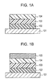
- Figs. 1A and 1B show examples of layer structures of electrophotographic photosensitive members.
- Fig. 2 shows an example of a schematic structure of an electrophotographic apparatus having a process cartridge including an electrophotographic photosensitive member according to aspects of the present invention.
- the compound represented by general formula (1) has a chemical structure in which aryl groups (Ar 1 and Ar 2 ) in the molecule easily face each other. It is believed that the distance between the aryl groups facing each other is decreased (the aryl groups overlap with each other) due to the external pressure that would cause scratches on an electrophotographic photosensitive member, whereby the aryl groups function as a kind of spring at a molecular level and thus the external pressure can be immediately converted into thermal energy that is generated through a change in chemical structure. It is also believed that the aryl groups facing each other function as a conductive path having anisotropy, and thus the degradation of electrical characteristics can be prevented.
- Urea compounds having an aryl group among those disclosed in Japanese Patent Laid-Open Nos. 58-065438 and 63-097959 do not have a structure in which short-chain alkyl groups (R 1 and R 2 : alkyl groups having 1 to 3 carbon atoms) are directly bonded to a nitrogen atom. Therefore, aryl groups do not overlap with each other. Thus, it is believed that the effect as a spring obtained from the overlap of aryl groups is not produced.
- An electrophotographic photosensitive member generally includes a support and a photosensitive layer formed on the support.
- the photosensitive layer of the electrophotographic photosensitive member may be a single-layer photosensitive layer ( Fig. 1A ) that includes a charge transporting layer and a charge generating layer in the same layer or may be a stacked photosensitive layer ( Fig. 1B ) that separately includes a charge generating layer containing a charge generating substance and a charge transporting layer containing a charge transporting substance.
- a stacked photosensitive layer is favorably used.
- 101 denotes a support
- 102 denotes an intermediate layer
- 103 denotes a charge generating layer
- 104 denotes a charge transporting layer
- 105 denotes a protective layer.
- a surface layer of the electrophotographic photosensitive member means a layer located at an outermost surface.
- the surface layer of the electrophotographic photosensitive member is a charge transporting layer 104.
- the surface layer of the electrophotographic photosensitive member is a protective layer 105.
- the surface layer of the electrophotographic photosensitive member comprises a cured resin obtained by polymerizing a compound having at least one polymerizable functional group.
- a polymerization initiator may be optionally used.
- the compound having at least one polymerizable functional group can be polymerized by using heat, light (e.g., ultraviolet light), or radiation (e.g., electron beam). Among them, the polymerization may be performed using radiation and even an electron beam because a polymerization initiator is not necessarily used if radiation is adopted.
- an electron beam may be applied in an inert gas atmosphere and heat treatment is then performed in an inert gas atmosphere to prevent the polymerization inhibition caused by oxygen.
- the inert gas include nitrogen and argon.
- the surface layer of the electrophotographic photosensitive member further comprises a compound (urea derivative, urea compound) represented by general formula (1) below.
- R 1 and R 2 are each independently an alkyl group having 1 to 3 carbon atoms.
- the alkyl group include a methyl group, an ethyl group, and a propyl group (n-propyl group or isopropyl group).
- R 1 and R 2 are hydrogen atoms, advantages according to aspects of the present invention are not achieved.
- R 1 and R 2 are each an alkyl group having 4 or more carbon atoms, R 1 and R 2 function as a factor that inhibits the formation of high-density structure (three-dimensional network structure) of a cured resin that constitutes the surface layer. Consequently, a surface layer having sufficient film strength is not obtained. If the film strength of the surface layer is insufficient, satisfactory wear resistance and scratch resistance are not achieved.
- R 1 and R 2 are each independently a substituted or unsubstituted aryl group.
- the substituted or unsubstituted aryl group include a substituted or unsubstituted phenyl group and a substituted or unsubstituted polycyclic aromatic group.
- the polycyclic aromatic group include a naphthyl group, a fluorene group, and a dimethylfluorene group.
- a substituent that may be included in the substituted or unsubstituted aryl group is limited to a carboxyl group, a cyano group, a substituted or unsubstituted amino group, a hydroxyl group, a substituted or unsubstituted alkoxy group, a substituted or unsubstituted alkyl group, a nitro group, and a halogen atom.
- Examples of the substituted amino group include a dimethylamino group and a diethylamino group.
- Examples of the substituted or unsubstituted alkoxy group include a methoxy group and an ethoxy group.
- Examples of the substituted or unsubstituted alkyl group include a methyl group, an ethyl group, a propyl group (n-propyl group or isopropyl group), and trifluoromethyl group.
- Examples of the halogen atom include a fluorine atom, a chlorine atom, and a bromine atom.
- the compound represented by general formula (1) can have a symmetrical structure in which R 1 and R 2 are the same group and Ar 1 and Ar 2 are the same group in general formula (1).
- the surface layer of the electrophotographic photosensitive member can contain the compound represented by general formula (1) in an amount of 1 to 20% by mass relative to the total mass of the surface layer. If the amount is excessively small, advantages according to aspects of the present invention may be degraded. If the amount is excessively large, a high-density structure (three-dimensional network structure) of a cured resin that constitutes the surface layer is not achieved and thus the film strength of the surface layer may be decreased, and the compound represented by general formula (1) may be precipitated from the surface layer.
- One or more of the compounds represented by general formula (1) may be contained in the surface layer of the electrophotographic photosensitive member.
- the compound represented by general formula (1) can be synthesized, for example, by the method described in the documents below.
- the compound represented by structural formula (U-1), the compound represented by structural formula (U-2), and the compound represented by structural formula (U-10) can be favorably used.
- the compounds represented by structural formulas (U-1) to (U-24) are also referred to as example compounds (U-1) to (U-24) .
- the compound having at least one polymerizable functional group and used for the surface layer of the electrophotographic photosensitive member according to aspects of the present invention is a compound that can form a cured resin through polymerization.
- the compound having at least one polymerizable functional group may be a charge transporting compound having a charge transporting structure in a molecule.
- the charge transporting structure include structures of triarylamine, hydrazone, pyrazoline, and carbazole.
- the compound having at least one polymerizable functional group may be a charge transporting compound having two or more polymerizable functional groups.
- the compound having at least one polymerizable functional group may be a compound represented by general formula (4) below.
- the compound represented by general formula (4) below has a monoamine structure with high polymerization efficiency. In the structure, the number of polymerizable functional groups, which easily increase the internal stress of the surface layer and thus easily cause scratches if excessively present, is appropriately adjusted.
- R 3 and R 4 are each independently a hydrogen atom or a methyl group and Ar 3 is a substituted or unsubstituted aryl group.
- m and n are each independently an integer of 0 to 5.
- the substituted or unsubstituted aryl group include a phenyl group, a naphthyl group, a fluorenyl group, and a 9,9-dimethylfluorenyl group.
- Ar 3 in general formula (4) is a substituted or unsubstituted phenyl group.
- the compound having at least one polymerizable functional group may be a compound represented by structural formula (5) below.
- the surface layer comprising a cured resin When the surface layer comprising a cured resin is formed, one or more of the compound having at least one polymerizable functional group may be used.
- Any support having conductivity may be used for the support of the electrophotographic photosensitive member.
- a support made of a metal such as aluminum, stainless steel, or nickel or a support made of a metal, plastic, or paper whose surface is coated with a conductive film can be used.
- the support can have a cylindrical or film-like shape or the like.
- a cylindrical support made of aluminum is suitable in terms of mechanical strength, electrophotographic characteristics, and cost.
- An open pipe may be used as a support without any treatment, but an open pipe whose surface is subjected to physical treatment such as cutting or honing, anodic oxidation treatment, or chemical treatment that uses an acid or the like may be used as a support.
- a support having a surface roughness Rz of 0.1 ⁇ m or more and 3.0 ⁇ m or less that is achieved by subjecting an open pipe to physical treatment such as cutting or honing has a satisfactory interference fringe-suppressing function.
- a conductive layer (not shown in Figs. 1A and 1B ) can be optionally formed between the support and the photosensitive layer or an intermediate layer described below.
- the conductive layer is not necessarily formed when the support itself has an interference fringe-suppressing function.
- an open pipe is used as a support without any treatment and a conductive layer is formed thereon, whereby an interference fringe-suppressing function can be easily imparted. Therefore, the conductive layer is quite useful in terms of productivity and cost.
- the conductive layer can be formed by the method below.
- a conductive layer-forming coating solution is prepared by dispersing inorganic particles of tin oxide, indium oxide, titanium oxide, barium sulfate, or the like in an appropriate solvent together with a curable resin such as a phenol resin and optionally by adding roughening particles.
- the coating solution is applied on the support, and the resultant film is dried by heating to form a conductive layer.
- the thickness of the conductive layer can be 10 ⁇ m or more and 30 ⁇ m or less.
- An intermediate layer may be formed on the support or the conductive layer to ensure adhesion between the support and a photosensitive layer, to protect a photosensitive layer from electrical breakdown, and to improve the carrier injection into a photosensitive layer.
- the intermediate layer can be formed by applying an intermediate layer-forming coating solution obtained by dissolving a resin in a solvent and then drying the coated film.
- the resin used for the intermediate layer examples include acrylic resins, allyl resins, alkyd resins, ethyl cellulose resins, ethylene-acrylic acid copolymers, epoxy resins, casein resins, silicone resins, gelatin resins, phenol resins, butyral resins, polyacrylate, polyacetal, polyamide-imide, polyamide, poly(allyl ether), polyimide, polyurethane, polyester, polyethylene, polycarbonate, polystyrene, polysulfone, polyvinyl alcohol, polybutadiene, polypropylene, urea resins, agarose resins, and cellulose resins.
- Examples of a solvent used for the intermediate layer-forming coating solution include benzene, toluene, xylene, tetralin, chlorobenzene, dichloromethane, chloroform, trichloroethylene, tetrachloroethylene, carbon tetrachloride, methyl acetate, ethyl acetate, propyl acetate, methyl formate, ethyl formate, acetone, methyl ethyl ketone, cyclohexanone, diethyl ether, dipropyl ether, propylene glycol monomethyl ether, dioxane, methylal, tetrahydrofuran, water, methanol, ethanol, n-propanol, isopropanol, butanol, methyl cellosolve, methoxypropanol, dimethylformamide, dimethylacetamide, and dimethyl sulfoxide.
- the thickness of the intermediate layer can be 0.1 ⁇ m or more and 5 ⁇ m or less.
- a photosensitive layer may be formed on the support, the conductive layer, or the intermediate layer.
- Examples of a charge generating substance include azo pigments such as monoazo, bisazo, trisazo, and tetrakisazo pigments; phthalocyanine pigments such as gallium phthalocyanine and oxytitanium phthalocyanine; and perylene pigments.
- azo pigments such as monoazo, bisazo, trisazo, and tetrakisazo pigments
- phthalocyanine pigments such as gallium phthalocyanine and oxytitanium phthalocyanine
- perylene pigments perylene pigments.
- gallium phthalocyanine is suitable in terms of characteristic stability in environmental variation.
- a hydroxygallium phthalocyanine crystal having strong peaks at Bragg angles 2 ⁇ of 7.4° ⁇ 0.3° and 28.2° ⁇ 0.3° in the X-ray diffraction spectrum measured using a CuK ⁇ characteristic X-ray may be used.
- examples of the binding resin used in the charge transporting layer include insulating resins such as polyvinyl butyral, polyarylate, polycarbonate, polyester, phenoxy resins, polyvinyl acetate, acrylic resins, polyacrylamide, polyvinylpyridine, cellulose resins, urethane resins, epoxy resins, agarose resins, casein, polyvinyl alcohol, and polyvinylpyrrolidone.
- organic photoconductive polymers such as poly-N-vinylcarbazole, polyvinyl anthracene, and polyvinyl pyrene can be used.
- Examples of a solvent used for a charge generating layer-forming coating solution include toluene, xylene, tetralin, chlorobenzene, dichloromethane, chloroform, trichloroethylene, tetrachloroethylene, carbon tetrachloride, methyl acetate, ethyl acetate, propyl acetate, methyl formate, ethyl formate, acetone, methyl ethyl ketone, cyclohexanone, diethyl ether, dipropyl ether, propylene glycol monomethyl ether, dioxane, methylal, tetrahydrofuran, water, methanol, ethanol, n-propanol, isopropanol, butanol, methyl cellosolve, methoxypropanol, dimethylformamide, dimethylacetamide, and dimethyl sulfoxide.
- the charge generating layer can be formed by applying a charge generating layer-forming coating solution containing the charge generating substance and optionally the binding resin, and then by drying the coated film.
- the charge generating layer-forming coating solution may be prepared by adding only the charge generating substance to a solvent and performing dispersion treatment and then by adding the binding resin, or may be prepared by adding the charge generating substance and the binding resin to a solvent at the same time and performing dispersion treatment.
- the thickness of the charge generating layer can be 0.05 ⁇ m or more and 5 ⁇ m or less.
- Examples of a charge transporting substance include triarylamine compounds, hydrazone compounds, stilbene compounds, pyrazoline compounds, oxazole compounds, thiazole compounds, and triarylmethane compounds.
- examples of the binding resin used in the charge transporting layer include insulating resins such as polyvinyl butyral, polyarylate, polycarbonate, polyester, phenoxy resins, polyvinyl acetate, acrylic resins, polyacrylamide, polyamide, polyvinylpyridine, cellulose resins, urethane resins, epoxy resins, agarose resins, casein, polyvinyl alcohol, and polyvinylpyrrolidone.
- organic photoconductive polymers such as poly-N-vinylcarbazole, polyvinyl anthracene, and polyvinyl pyrene can be used.
- Examples of a solvent used for a charge transporting layer-forming coating solution include toluene, xylene, tetralin, chlorobenzene, dichloromethane, chloroform, trichloroethylene, tetrachloroethylene, carbon tetrachloride, methyl acetate, ethyl acetate, propyl acetate, methyl formate, ethyl formate, acetone, methyl ethyl ketone, cyclohexanone, diethyl ether, dipropyl ether, propylene glycol monomethyl ether, dioxane, methylal, tetrahydrofuran, water, methanol, ethanol, n-propanol, isopropanol, butanol, methyl cellosolve, methoxypropanol, dimethylformamide, dimethylacetamide, and dimethyl sulfoxide.
- the charge transporting layer can be formed by applying a charge transporting layer-forming coating solution obtained by dissolving the charge transporting substance and optionally the binding resin in a solvent, and then by drying the coated film.
- the thickness of the charge transporting layer can be 5 ⁇ m or more and 40 ⁇ m or less.
- the surface layer of the electrophotographic photosensitive member according to aspects of the present invention has the above-described structure.
- Conductive particles, an ultraviolet absorber, a wear resistance improver may be further added to the surface layer.
- An example of the conductive particles is a metal oxide such as tin oxide particles.
- Examples of the wear resistance improver include fluorine-containing resin particles, alumina particles, and silica particles.
- the thickness of the surface layer can be 0.5 ⁇ m or more and 20 ⁇ m or less.
- Examples of a solvent used for a surface layer-forming coating solution include toluene, xylene, tetralin, chlorobenzene, dichloromethane, chloroform, trichloroethylene, tetrachloroethylene, carbon tetrachloride, methyl acetate, ethyl acetate, propyl acetate, methyl formate, ethyl formate, acetone, methyl ethyl ketone, cyclohexanone, diethyl ether, dipropyl ether, propylene glycol monomethyl ether, dioxane, methylal, tetrahydrofuran, water, methanol, ethanol, n-propanol, isopropanol, butanol, 1,1,2,2,3,3,4-heptafluorocyclopentane, 4-methylmorpholine, N,N'-dimethylcyclohexylamine, methyl cellosolve, me
- a surface layer having charge transportability is formed on the charge generating layer.
- a surface layer is formed on the charge transporting layer.
- Each of the above-described layers can be formed by a coating method such as dip coating (dipping), spray coating, spinner coating, bead coating, blade coating, or beam coating.
- a coating method such as dip coating (dipping), spray coating, spinner coating, bead coating, blade coating, or beam coating.
- Fig. 2 shows an example of a schematic structure of an electrophotographic apparatus having a process cartridge including the electrophotographic photosensitive member according to aspects of the present invention.
- a drum-shaped electrophotographic photosensitive member 1 is rotated about a shaft 2 at a predetermined peripheral speed (processing speed) in a direction indicated by an arrow.
- the peripheral surface of the electrophotographic photosensitive member 1 is uniformly charged at a predetermined positive or negative potential by charging means (first charging means) 3.
- the electrophotographic photosensitive member 1 is irradiated with exposure light 4 that is output from exposure means (not shown) providing slit exposure or laser beam scanning exposure and that is intensity-modulated in accordance with a time-series electrical digital pixel signal of intended image information.
- exposure means not shown
- the formed electrostatic latent image is developed as a toner image with toner contained in developing means 5, by normal or reversal developing.
- the toner image formed and carried on the surface of the electrophotographic photosensitive member 1 is then sequentially transferred onto a transfer medium 7 by transferring means 6.
- the transfer medium 7 is fed from a feeding unit (not shown) into a portion between the electrophotographic photosensitive member 1 and the transferring means 6 in synchronization with the rotation of the electrophotographic photosensitive member 1.
- a bias voltage having a polarity opposite to the charge polarity of the toner is applied to the transferring means 6 from a bias power source (not shown).
- the transferring means may adopt an intermediate transferring system, in which the transferring means is constituted by a first transfer member, an intermediate transfer body, and a second transfer member.
- the transfer medium 7 on which the toner image has been transferred is separated from the surface of the electrophotographic photosensitive member and conveyed to fixing means 8 where the toner image is subjected to a fixing process. After the fixing process, the transfer medium 7 is printed out as an image-formed matter (print or copy) to the outside of the electrophotographic apparatus.
- the toner left without being transferred can be collected by a developing unit or the like.
- the electrophotographic photosensitive member 1 is decharged by pre-exposure light 10 from pre-exposure means (not shown), and is then repeatedly used for image formation.
- pre-exposure is not necessarily required.
- two or more of the components may be accommodated in a container to constitute a process cartridge.
- the process cartridge may be detachably installed in the main body of an electrophotographic apparatus such as a copying machine or a laser beam printer.
- at least one means selected from the charging means 3, the developing means 5, the transferring means 6, and the cleaning means 9 can be integrally supported together with the electrophotographic photosensitive member 1 to constitute a process cartridge 11, which is detachably installed in the main body of the electrophotographic apparatus by using guiding means 12 such as a rail of the main body of the electrophotographic apparatus.
- titanium oxide particles coated with tin oxide that contains 10% antimony oxide, 25 parts of resole phenolic resin, 20 parts of methyl cellosolve, 5 parts of methanol, and 0.002 parts of silicone oil (polydimethylsiloxane-polyoxyalkylene copolymer with an average molecular weight of 3000) were dispersed for 2 hours with a sand mill device that uses glass beads having a diameter of 0.8 mm to prepare a conductive layer-forming coating solution.
- the conductive layer-forming coating solution was applied by dipping on an aluminum cylinder (drawn tube having an outer diameter of 30 mm) serving as the support, and the resultant film was dried at 140°C for 30 minutes to form a conductive layer having a thickness of 15 ⁇ m.
- nylon 6-66-610-12 quaternary nylon copolymer resin product name: CM8000 manufactured by Toray Industries, Inc.
- 7.5 parts of N-methoxymethylated 6-nylon resin product name: Toresin EF-30T manufactured by Nagase ChemteX Corporation
- the intermediate layer-forming coating solution was applied on the conductive layer by dipping, and the resultant film was dried at 100°C for 10 minutes to form an intermediate layer having a thickness of 0.55 ⁇ m.
- hydroxygallium phthalocyanine crystals charge generating substance having strong peaks at Bragg angles of 7.4° and 28.2° in the X-ray diffraction spectrum measured using a CuK ⁇ characteristic X-ray were added to a solution obtained by dissolving 5 parts of polyvinyl butyral (product name: S-LEC BX-1 manufactured by Sekisui Chemical Co., Ltd.) in 130 parts of cyclohexanone.
- Five hundred parts of glass beads having a diameter of 1 mm were added thereto, and dispersion treatment was performed at 1800 rpm for 2 hours while the resultant solution was cooled with a 18°C cooling water.
- the solution subjected to the dispersion treatment was diluted with 300 parts of ethyl acetate and 160 parts of cyclohexanone to prepare a charge generating layer-forming coating solution.
- the average particle size (median) of the hydroxygallium phthalocyanine crystals contained in the charge generating layer-forming coating solution was measured with a centrifugal particle size analyzer (product name: CAPA700 manufactured by HORIBA, Ltd.) that uses liquid phase precipitation as a basic principle.
- the average particle size was 0.10 ⁇ m.
- the charge generating layer-forming coating solution was applied on the intermediate layer by dipping, and the resultant film was dried at 110°C for 10 minutes to form a charge generating layer having a thickness of 0.14 ⁇ m.
- the charge transporting layer-forming coating solution was applied on the charge generating layer by dipping, and the resultant film was dried at 100°C for 30 minutes to form a charge transporting layer having a thickness of 17 ⁇ m.
- the protective layer-forming coating solution was applied on the charge transporting layer by dipping, and then heated at 50°C for 5 minutes.
- the resultant film was irradiated with an electron beam for 1.5 seconds at an acceleration voltage of 80 kV at an absorbed dose of 19000 Gy in a nitrogen atmosphere.
- the film was then heated at 125°C in a nitrogen atmosphere for 30 seconds.
- the oxygen concentration from the irradiation with an electron beam to the 30-second heat treatment was 19 ppm.
- heat treatment was performed at 100°C in the air for 20 minutes to form a protective layer having a thickness of 4.8 ⁇ m.
- an electrophotographic photosensitive member including the support, the conductive layer, the intermediate layer, the charge generating layer, the charge transporting layer, and the protective layer, which is the surface layer, was produced.
- This electrophotographic photosensitive member is referred to as an electrophotographic photosensitive member 1.
- An electrophotographic photosensitive member was produced in the same manner as in Example 1, except that, in Example 1, the protective layer-forming coating solution was prepared by changing the amount of the compound represented by structural formula (5) to 48.5 parts and the amount of the example compound (U-1) to 1.5 parts.
- This electrophotographic photosensitive member is referred to as an electrophotographic photosensitive member 2.
- An electrophotographic photosensitive member was produced in the same manner as in Example 1, except that, in Example 1, the protective layer-forming coating solution was prepared by changing the amount of the compound represented by structural formula (5) to 42.5 parts and the amount of the example compound (U-1) to 7.5 parts.
- This electrophotographic photosensitive member is referred to as an electrophotographic photosensitive member 3.
- An electrophotographic photosensitive member was produced in the same manner as in Example 1, except that, in Example 1, the protective layer-forming coating solution was prepared by changing the amount of the compound represented by structural formula (5) to 39 parts and the amount of the example compound (U-1) to 11 parts.
- This electrophotographic photosensitive member is referred to as an electrophotographic photosensitive member 4.
- This is referred to as
- An electrophotographic photosensitive member was produced in the same manner as in Example 1, except that, in Example 1, the example compound (U-1) was changed to the example compound (U-2) (manufactured by TOKYO CHEMICAL INDUSTRY Co., Ltd., GC purity: > 98%). This is referred to as an electrophotographic photosensitive member 6.
- An electrophotographic photosensitive member was produced in the same manner as in Example 1, except that, in Example 2, the example compound (U-1) was changed to the example compound (U-2) (manufactured by TOKYO CHEMICAL INDUSTRY Co., Ltd., GC purity: > 98%). This is referred to as an electrophotographic photosensitive member 7.
- An electrophotographic photosensitive member was produced in the same manner as in Example 1, except that, in Example 3, the example compound (U-1) was changed to the example compound (U-2) (manufactured by TOKYO CHEMICAL INDUSTRY Co., Ltd., GC purity: > 98%). This is referred to as an electrophotographic photosensitive member 8.
- An electrophotographic photosensitive member was produced in the same manner as in Example 1, except that, in Example 4, the example compound (U-1) was changed to the example compound (U-2) (manufactured by TOKYO CHEMICAL INDUSTRY Co., Ltd., GC purity: > 98%). This is referred to as an electrophotographic photosensitive member 9.
- An electrophotographic photosensitive member was produced in the same manner as in Example 1, except that, in Example 5, the example compound (U-1) was changed to the example compound (U-2) (manufactured by TOKYO CHEMICAL INDUSTRY Co., Ltd., GC purity: > 98%). This is referred to as an electrophotographic photosensitive member 10.
- a protective layer-forming coating solution was prepared by further adding 2.5 parts of 1-hydroxycyclohexyl phenyl ketone (product name: Irgacure 184 manufactured by Ciba Specialty Chemicals, photopolymerization initiator) to the protective layer-forming coating solution prepared in Example 2.
- This protective layer-forming coating solution was applied on the charge transporting layer by dipping and then heated at 50°C for 5 minutes.
- the resultant film was irradiated with light using a metal halide lamp at an irradiation intensity of 500 mW/cm 2 for 20 seconds and heated at 130°C for 30 minutes to form a protective layer (surface layer) having a thickness of 4.8 ⁇ m.
- An electrophotographic photosensitive member was produced in the same manner as in Example 2, except for the above-described treatment. This is referred to as an electrophotographic photosensitive member 11.
- An electrophotographic photosensitive member was produced in the same manner as in Example 11, except that, in Example 11, the example compound (U-1) was changed to the example compound (U-2) (manufactured by TOKYO CHEMICAL INDUSTRY Co., Ltd., GC purity: > 98%). This is referred to as an electrophotographic photosensitive member 12.
- An electrophotographic photosensitive member was produced in the same manner as in Example 2, except that, in Example 2, the compound represented by structural formula (5) above was changed to a compound represented by structural formula (8) below. This is referred to as an electrophotographic photosensitive member 13.
- An electrophotographic photosensitive member was produced in the same manner as in Example 13, except that, in Example 13, the example compound (U-1) was changed to the example compound (U-2) (manufactured by TOKYO CHEMICAL INDUSTRY Co., Ltd., GC purity: > 98%). This is referred to as an electrophotographic photosensitive member 14.
- An electrophotographic photosensitive member was produced in the same manner as in Example 2, except that, in Example 2, the compound represented by structural formula (5) above was changed to a compound represented by structural formula (9) below. This is referred to as an electrophotographic photosensitive member 15.
- An electrophotographic photosensitive member was produced in the same manner as in Example 15, except that, in Example 15, the example compound (U-1) was changed to the example compound (U-2) (manufactured by TOKYO CHEMICAL INDUSTRY Co., Ltd., GC purity: > 98%). This is referred to as an electrophotographic photosensitive member 16.
- An electrophotographic photosensitive member was produced in the same manner as in Example 2, except that, in Example 2, the compound represented by structural formula (5) above was changed to a compound represented by structural formula (10) below. This is referred to as an electrophotographic photosensitive member 17.
- An electrophotographic photosensitive member was produced in the same manner as in Example 17, except that, in Example 17, the example compound (U-1) was changed to the example compound (U-2) (manufactured by TOKYO CHEMICAL INDUSTRY Co., Ltd., GC purity: > 98%). This is referred to as an electrophotographic photosensitive member 18.
- the protective layer-forming coating solution of Example 2 was changed to a protective layer-forming coating solution obtained by dissolving 24.5 parts of dipentaerythritol hexaacrylate (product name: DPHA manufactured by DAICEL-CYTEC Company, Ltd.) (a compound having six acrylic groups, which are polymerizable functional groups, and having no charge transporting structure), 24 parts of a compound represented by structural formula (11), 2.5 parts of 1-hydroxycyclohexyl phenyl ketone (product name: Irgacure 184 manufactured by Ciba Specialty Chemicals, photopolymerization initiator), and 1.5 parts of the example compound (U-1) in 25 parts of n-propanol and then by further adding 25 parts of 1,1,2,2,3,3,4-heptafluorocyclopentane (product name: ZEORORA H manufactured by ZEON Corporation).
- dipentaerythritol hexaacrylate product name: DPHA manufactured by DAICEL-CYTEC Company, Ltd
- This protective layer-forming coating solution was applied on the charge transporting layer by dipping and then heated at 50°C for 5 minutes.
- the resultant film was irradiated with light using a metal halide lamp at an irradiation intensity of 500 mW/cm 2 for 20 seconds and heated at 130°C for 30 minutes to form a protective layer (surface layer) having a thickness of 4.8 ⁇ m.
- An electrophotographic photosensitive member was produced in the same manner as in Example 2, except for the above-described treatment. This is referred to as an electrophotographic photosensitive member 19.
- An electrophotographic photosensitive member was produced in the same manner as in Example 19, except that, in Example 19, the example compound (U-1) was changed to the example compound (U-2) (manufactured by TOKYO CHEMICAL INDUSTRY Co., Ltd., GC purity: > 98%). This is referred to as an electrophotographic photosensitive member 20.
- the protective layer-forming coating solution of Example 2 was changed to a protective layer-forming coating solution obtained by dispersing 50 parts of tin oxide ultra-fine particles doped with antimony and surface-treated with a compound represented by structural formula (12) (the amount treated: 7%) and 150 parts of ethanol using a sand mill for 66 hours, further adding 20 parts of polytetrafluoroethylene particles (average particle size: 0.18 ⁇ m), dispersing the mixture for 2 hours, and dissolving 25 parts of resole phenolic resin (product name: PL-4804 manufactured by Gun Ei Chemical Industry Co., Ltd. and containing amine compounds other than ammonia) therein.
- a protective layer-forming coating solution obtained by dispersing 50 parts of tin oxide ultra-fine particles doped with antimony and surface-treated with a compound represented by structural formula (12) (the amount treated: 7%) and 150 parts of ethanol using a sand mill for 66 hours, further adding 20 parts of polytetrafluoroethylene particles (average particle size
- This protective layer-forming coating solution was applied on the charge transporting layer by dipping, and the resultant film was heated at 150°C for 60 minutes to form a protective layer (surface layer) having a thickness of 4.8 ⁇ m.
- An electrophotographic photosensitive member was produced in the same manner as in Example 2, except for the above-described treatment. This is referred to as an electrophotographic photosensitive member 21.
- An electrophotographic photosensitive member was produced in the same manner as in Example 21, except that, in Example 21, the example compound (U-1) was changed to the example compound (U-2) (manufactured by TOKYO CHEMICAL INDUSTRY Co., Ltd., GC purity: > 98%). This is referred to as an electrophotographic photosensitive member 22.
- An electrophotographic photosensitive member was produced in the same manner as in Example 2, except that, in Example 2, the example compound (U-1) was changed to an example compound (U-3) synthesized in accordance with the method described in Photochem. Photobiol. Sci., 2002, 1, 30-37. This is referred to as an electrophotographic photosensitive member 23.
- An electrophotographic photosensitive member was produced in the same manner as in Example 2, except that, in Example 2, the example compound (U-1) was changed to an example compound (U-4) synthesized in accordance with the method described in Photochem. Photobiol. Sci., 2002, 1, 30-37 . This is referred to as an electrophotographic photosensitive member 24.
- An electrophotographic photosensitive member was produced in the same manner as in Example 2, except that, in Example 2, the example compound (U-1) was changed to an example compound (U-6) synthesized in accordance with the method described in Photochem. Photobiol. Sci., 2002, 1, 30-37 . This is referred to as an electrophotographic photosensitive member 25.
- An electrophotographic photosensitive member was produced in the same manner as in Example 2, except that, in Example 2, the example compound (U-1) was changed to an example compound (U-8) synthesized in accordance with the method described in Photochem. Photobiol. Sci., 2002, 1, 30-37 . This is referred to as an electrophotographic photosensitive member 26.
- An electrophotographic photosensitive member was produced in the same manner as in Example 2, except that, in Example 2, the example compound (U-1) was changed to an example compound (U-9) synthesized in accordance with the method described in Photochem. Photobiol. Sci., 2002, 1, 30-37 . This is referred to as an electrophotographic photosensitive member 27.
- An electrophotographic photosensitive member was produced in the same manner as in Example 2, except that, in Example 2, the example compound (U-1) was changed to an example compound (U-10) synthesized in accordance with the method described in Photochem. Photobiol. Sci., 2002, 1, 30-37 . This is referred to as an electrophotographic photosensitive member 28.
- An electrophotographic photosensitive member was produced in the same manner as in Example 2, except that, in Example 2, the example compound (U-1) was changed to an example compound (U-12) synthesized in accordance with the method described in Photochem. Photobiol. Sci., 2002, 1, 30-37 . This is referred to as an electrophotographic photosensitive member 29.
- An electrophotographic photosensitive member was produced in the same manner as in Example 2, except that, in Example 2, the example compound (U-1) was changed to an example compound (U-13) synthesized in accordance with the method described in Photochem. Photobiol. Sci., 2002, 1, 30-37 . This is referred to as an electrophotographic photosensitive member 30.
- An electrophotographic photosensitive member was produced in the same manner as in Example 2, except that, in Example 2, the example compound (U-1) was changed to an example compound (U-15) synthesized in accordance with the method described in Photochem. Photobiol. Sci., 2002, 1, 30-37 . This is referred to as an electrophotographic photosensitive member 31.
- An electrophotographic photosensitive member was produced in the same manner as in Example 2, except that, in Example 2, the example compound (U-1) was changed to an example compound (U-19) synthesized in accordance with the method described in Photochem. Photobiol. Sci., 2002, 1, 30-37 . This is referred to as an electrophotographic photosensitive member 32.
- An electrophotographic photosensitive member was produced in the same manner as in Example 2, except that, in Example 2, the example compound (U-1) was changed to an example compound (U-20) synthesized in accordance with the method described in Photochem. Photobiol. Sci., 2002, 1, 30-37 . This is referred to as an electrophotographic photosensitive member 33.
- An electrophotographic photosensitive member was produced in the same manner as in Example 2, except that, in Example 2, the example compound (U-1) was changed to an example compound (U-21) synthesized in accordance with the method described in Photochem. Photobiol. Sci., 2002, 1, 30-37 . This is referred to as an electrophotographic photosensitive member 34.
- An electrophotographic photosensitive member was produced in the same manner as in Example 2, except that, in Example 2, the example compound (U-1) was changed to an example compound (U-22) synthesized in accordance with the method described in Photochem. Photobiol. Sci., 2002, 1, 30-37 . This is referred to as an electrophotographic photosensitive member 35.
- An electrophotographic photosensitive member was produced in the same manner as in Example 2, except that, in Example 2, the example compound (U-1) was changed to an example compound (U-23) synthesized in accordance with the method described in Photochem. Photobiol. Sci., 2002, 1, 30-37 . This is referred to as an electrophotographic photosensitive member 36.
- An electrophotographic photosensitive member was produced in the same manner as in Example 2, except that, in Example 2, the example compound (U-1) was changed to an example compound (U-24) synthesized in accordance with the method described in Photochem. Photobiol. Sci., 2002, 1, 30-37 . This is referred to as an electrophotographic photosensitive member 37.
- An electrophotographic photosensitive member was produced in the same manner as in Example 2, except that, in Example 2, the example compound (U-1) was changed to a compound represented by structural formula (13) below. This is referred to as an electrophotographic photosensitive member C1.
- An electrophotographic photosensitive member was produced in the same manner as in Example 2, except that, in Example 2, the example compound (U-1) was changed to a compound represented by structural formula (14) below. This is referred to as an electrophotographic photosensitive member C2.
- An electrophotographic photosensitive member was produced in the same manner as in Example 2, except that, in Example 2, the example compound (U-1) was changed to a compound represented by structural formula (15) below. This is referred to as an electrophotographic photosensitive member C3.
- An electrophotographic photosensitive member was produced in the same manner as in Example 2, except that, in Example 2, the example compound (U-1) was changed to a compound represented by structural formula (16) below. This is referred to as an electrophotographic photosensitive member C4.
- An electrophotographic photosensitive member was produced in the same manner as in Example 2, except that, in Example 2, the example compound (U-1) was changed to a compound represented by structural formula (17) below. This is referred to as an electrophotographic photosensitive member C5.
- An electrophotographic photosensitive member was produced in the same manner as in Example 2, except that, in Example 2, the example compound (U-1) was changed to a compound represented by structural formula (18) below. This is referred to as an electrophotographic photosensitive member C6.
- An electrophotographic photosensitive member was produced in the same manner as in Example 2, except that, in Example 2, the example compound (U-1) was changed to a compound represented by structural formula (19) below. This is referred to as an electrophotographic photosensitive member C7.
- An electrophotographic photosensitive member was produced in the same manner as in Example 2, except that, in Example 2, the example compound (U-1) was changed to a compound represented by structural formula (20) below. This is referred to as an electrophotographic photosensitive member C8.
- An electrophotographic photosensitive member was produced in the same manner as in Example 2, except that, in Example 2, the example compound (U-1) was changed to diethyl phthalate (plasticizer). This is referred to as an electrophotographic photosensitive member C9.
- An electrophotographic photosensitive member was produced in the same manner as in Example 2, except that, in Example 2, the example compound (U-1) was changed to a compound represented by structural formula (21) below. This is referred to as an electrophotographic photosensitive member C10.
- An electrophotographic photosensitive member was produced in the same manner as in Example 11, except that, in Example 11, the example compound (U-1) was changed to the compound represented by structural formula (21) above. This is referred to as an electrophotographic photosensitive member C11.
- An electrophotographic photosensitive member was produced in the same manner as in Example 13, except that, in Example 13, the example compound (U-1) was changed to the compound represented by structural formula (21) above. This is referred to as an electrophotographic photosensitive member C12.
- An electrophotographic photosensitive member was produced in the same manner as in Example 15, except that, in Example 15, the example compound (U-1) was changed to the compound represented by structural formula (21) above. This is referred to as an electrophotographic photosensitive member C13.
- An electrophotographic photosensitive member was produced in the same manner as in Example 17, except that, in Example 17, the example compound (U-1) was changed to the compound represented by structural formula (21) above. This is referred to as an electrophotographic photosensitive member C14.
- An electrophotographic photosensitive member was produced in the same manner as in Example 19, except that, in Example 19, the example compound (U-1) was changed to the compound represented by structural formula (21) above. This is referred to as an electrophotographic photosensitive member C15.
- An electrophotographic photosensitive member was produced in the same manner as in Example 21, except that, in Example 21, the example compound (U-1) was changed to the compound represented by structural formula (21) above. This is referred to as an electrophotographic photosensitive member C16.
- An electrophotographic photosensitive member was produced in the same manner as in Example 2, except that, in Example 2, the example compound (U-1) was not used. This is referred to as an electrophotographic photosensitive member C17.
- An electrophotographic photosensitive member was produced in the same manner as in Example 11, except that, in Example 11, the example compound (U-1) was not used. This is referred to as an electrophotographic photosensitive member C18.
- An electrophotographic photosensitive member was produced in the same manner as in Example 13, except that, in Example 13, the example compound (U-1) was not used. This is referred to as an electrophotographic photosensitive member C19.
- An electrophotographic photosensitive member was produced in the same manner as in Example 15, except that, in Example 15, the example compound (U-1) was not used. This is referred to as an electrophotographic photosensitive member C20.
- An electrophotographic photosensitive member was produced in the same manner as in Example 17, except that, in Example 17, the example compound (U-1) was not used. This is referred to as an electrophotographic photosensitive member C21.
- An electrophotographic photosensitive member was produced in the same manner as in Example 19, except that, in Example 19, the example compound (U-1) was not used. This is referred to as an electrophotographic photosensitive member C22.
- An electrophotographic photosensitive member was produced in the same manner as in Example 21, except that, in Example 21, the example compound (U-1) was not used. This is referred to as an electrophotographic photosensitive member C23.
- An electrophotographic photosensitive member was produced in the same manner as in Example 1, except that, in Example 1, the protective layer was not formed.
- the electrophotographic photosensitive member whose charge transporting layer is a surface layer is referred to as an electrophotographic photosensitive member C24.
- An electrophotographic photosensitive member was produced in the same manner as in Comparative Example 24, except that a charge transporting layer-forming coating solution obtained by further adding 0.6 parts of the example compound (U-1) to the charge transporting layer-forming coating solution prepared in Comparative Example 24 was used.
- the electrophotographic photosensitive member whose charge transporting layer is a surface layer is referred to as an electrophotographic photosensitive member C25.
- the universal hardness and elastic deformation ratio of the surface layer of each of the electrophotographic photosensitive members 2, 7, C10, and C17 were measured with a hardness meter (product name: H100VP-HCU manufactured by Fischer Instrumentation Ltd. in Germany).
- a quadrangular pyramid diamond indenter (the angle between opposite faces was 136°) was pressed into a surface layer to be measured while a load was applied to the diamond indenter.
- the indentation depth while a load was applied to the diamond indenter was electrically detected. The measurement was performed in an environment of 23°C/50 %RH.
- the universal hardness was determined by dividing the test load (final load: 2 mN) by the surface area of an indentation (calculated from the geometrical shape of the indenter) generated due to the test load.
- the elastic deformation ratio was determined by measuring the indentation depth and load until the load reached 0 by decreasing the test load (final load: 2 mN).
- Each of the electrophotographic photosensitive members 1 to 37 and C1 to C25 was installed in an electrophotographic copying machine (product name: iR4570 manufactured by CANON KABUSHIKI KAISHA).
- the dark potential was set to be -750 V
- the light potential was set to be -160 V
- a durability test for 200000 sheets of paper feeding was performed in an environment of 27°C/75 %RH.
- the presence or absence of image defects (damaged images) caused by the scratches formed on the surface of the electrophotographic photosensitive member was confirmed for every 10000 sheets through visual inspection (Examples 1 to 37 and Comparative Examples 1 to 25).
- the abrasion loss ( ⁇ m) of the surface layer after 50000 sheets of paper feeding was confirmed (Examples 1 to 10 and 23 to 37 and Comparative Examples 1 to 10 and 17). Table shows the results.
- 24 - - Damaged image is formed after 180000 sheets 0.10 30 Ex. 25 25 - - Damaged image is formed after 180000 sheets 0.10 35 Ex. 26 26 - - Damaged image is formed after 180000 sheets 0.15 30 Ex. 27 27 - - Damaged image is formed after 180000 sheets 0.10 35 Ex. 28 28 - - Damaged image is not formed even after 200000 sheets 0.15 30 Ex. 29 29 - - Damaged image is formed after 180000 sheets 0.15 35 Ex. 30 30 - - Damaged image is formed after 180000 sheets 0.15 30 Ex. 31 31 - - Damaged image is formed after 180000 sheets 0.15 30 Ex. 32 32 - - Damaged image is formed after 180000 sheets 0.10 30 Ex.
- an electrophotographic photosensitive member (1) includes a surface layer comprising a cured resin obtained by polymerizing a compound having at least one polymerizable functional group.
- aspects of the present invention provide an electrophotographic photosensitive member whose surface layer comprises a compound (urea derivative) having a certain structure, a method for producing the electrophotographic photosensitive member, and a process cartridge (11) and an electrophotographic apparatus including the electrophotographic photosensitive member.
Landscapes
- Physics & Mathematics (AREA)
- General Physics & Mathematics (AREA)
- Spectroscopy & Molecular Physics (AREA)
- Chemical & Material Sciences (AREA)
- Chemical Kinetics & Catalysis (AREA)
- Photoreceptors In Electrophotography (AREA)
Applications Claiming Priority (1)
| Application Number | Priority Date | Filing Date | Title |
|---|---|---|---|
| JP2009270098 | 2009-11-27 |
Publications (2)
| Publication Number | Publication Date |
|---|---|
| EP2328032A2 true EP2328032A2 (fr) | 2011-06-01 |
| EP2328032A3 EP2328032A3 (fr) | 2012-08-15 |
Family
ID=43579530
Family Applications (1)
| Application Number | Title | Priority Date | Filing Date |
|---|---|---|---|
| EP10186596A Withdrawn EP2328032A3 (fr) | 2009-11-27 | 2010-10-05 | Élément photosensible électrophotographique, son procédé de production, cartouche de traitement et appareil électrophotographique |
Country Status (1)
| Country | Link |
|---|---|
| EP (1) | EP2328032A3 (fr) |
Cited By (4)
| Publication number | Priority date | Publication date | Assignee | Title |
|---|---|---|---|---|
| EP2527922A1 (fr) * | 2011-05-24 | 2012-11-28 | Canon Kabushiki Kaisha | Élément photosensible électrophotographique, son procédé de production, cartouche de traitement, appareil électrophotographique et composé d'urée |
| US8859172B2 (en) | 2011-11-30 | 2014-10-14 | Canon Kabushiki Kaisha | Electrophotographic photosensitive member, method of producing electrophotographic photosensitive member, process cartridge, and electrophotographic apparatus |
| US8859174B2 (en) | 2011-05-24 | 2014-10-14 | Canon Kabushiki Kaisha | Electrophotographic photosensitive member, process cartridge, and electrophotographic apparatus |
| CN107765516A (zh) * | 2016-08-17 | 2018-03-06 | 富士施乐株式会社 | 电子照相感光体、处理盒和图像形成装置 |
Citations (5)
| Publication number | Priority date | Publication date | Assignee | Title |
|---|---|---|---|---|
| JPS5865438A (ja) | 1981-10-15 | 1983-04-19 | Fuji Photo Film Co Ltd | 光導電性組成物およびそれを用いた電子写真感光材料 |
| JPS6397959A (ja) | 1986-10-14 | 1988-04-28 | Konica Corp | 電子写真感光体 |
| JP2007272191A (ja) | 2006-03-10 | 2007-10-18 | Ricoh Co Ltd | 電子写真感光体およびそれを用いた画像形成方法、並びに画像形成装置、画像形成装置用プロセスカートリッジ |
| JP2007272192A (ja) | 2006-03-10 | 2007-10-18 | Ricoh Co Ltd | 電子写真感光体およびそれを用いた画像形成方法、並びに画像形成装置、画像形成装置用プロセスカートリッジ |
| JP2007279678A (ja) | 2006-03-14 | 2007-10-25 | Ricoh Co Ltd | 電子写真感光体およびそれを用いた画像形成方法、並びに画像形成装置、画像形成装置用プロセスカートリッジ |
Family Cites Families (1)
| Publication number | Priority date | Publication date | Assignee | Title |
|---|---|---|---|---|
| EP0964309B1 (fr) * | 1998-06-12 | 2005-12-07 | Canon Kabushiki Kaisha | Elément photosensible électrophotographique, cartouche de traitement et appareil électrophotographique, ainsi que procédé de fabrication de l' élément photosensible |
-
2010
- 2010-10-05 EP EP10186596A patent/EP2328032A3/fr not_active Withdrawn
Patent Citations (5)
| Publication number | Priority date | Publication date | Assignee | Title |
|---|---|---|---|---|
| JPS5865438A (ja) | 1981-10-15 | 1983-04-19 | Fuji Photo Film Co Ltd | 光導電性組成物およびそれを用いた電子写真感光材料 |
| JPS6397959A (ja) | 1986-10-14 | 1988-04-28 | Konica Corp | 電子写真感光体 |
| JP2007272191A (ja) | 2006-03-10 | 2007-10-18 | Ricoh Co Ltd | 電子写真感光体およびそれを用いた画像形成方法、並びに画像形成装置、画像形成装置用プロセスカートリッジ |
| JP2007272192A (ja) | 2006-03-10 | 2007-10-18 | Ricoh Co Ltd | 電子写真感光体およびそれを用いた画像形成方法、並びに画像形成装置、画像形成装置用プロセスカートリッジ |
| JP2007279678A (ja) | 2006-03-14 | 2007-10-25 | Ricoh Co Ltd | 電子写真感光体およびそれを用いた画像形成方法、並びに画像形成装置、画像形成装置用プロセスカートリッジ |
Non-Patent Citations (4)
| Title |
|---|
| BULLETIN OF THE CHEMICAL SOCIETY OF JAPAN, vol. 47, no. 4, 1974, pages 935 - 937 |
| PHOTOCHEM. PHOTOBIOL. SCI., vol. 1, 2002, pages 30 - 37 |
| TETRAHEDRON LETTERS, vol. 39, 1998, pages 6267 - 6270 |
| TRANSACTIONS OF THE FARADAY SOCIETY, vol. 34, 1938, pages 783 - 786 |
Cited By (6)
| Publication number | Priority date | Publication date | Assignee | Title |
|---|---|---|---|---|
| EP2527922A1 (fr) * | 2011-05-24 | 2012-11-28 | Canon Kabushiki Kaisha | Élément photosensible électrophotographique, son procédé de production, cartouche de traitement, appareil électrophotographique et composé d'urée |
| US8859174B2 (en) | 2011-05-24 | 2014-10-14 | Canon Kabushiki Kaisha | Electrophotographic photosensitive member, process cartridge, and electrophotographic apparatus |
| US8962227B2 (en) | 2011-05-24 | 2015-02-24 | Canon Kabushiki Kaisha | Electrophotographic photosensitive member, process cartridge, electrophotographic apparatus, method of producing electrophotographic photosensitive member, and urea compound |
| US8859172B2 (en) | 2011-11-30 | 2014-10-14 | Canon Kabushiki Kaisha | Electrophotographic photosensitive member, method of producing electrophotographic photosensitive member, process cartridge, and electrophotographic apparatus |
| CN107765516A (zh) * | 2016-08-17 | 2018-03-06 | 富士施乐株式会社 | 电子照相感光体、处理盒和图像形成装置 |
| CN107765516B (zh) * | 2016-08-17 | 2022-09-16 | 富士胶片商业创新有限公司 | 电子照相感光体、处理盒和图像形成装置 |
Also Published As
| Publication number | Publication date |
|---|---|
| EP2328032A3 (fr) | 2012-08-15 |
Similar Documents
| Publication | Publication Date | Title |
|---|---|---|
| US8993204B2 (en) | Electrophotographic photosensitive member, method for producing the same, process cartridge, and electrophotographic apparatus | |
| EP2633369B1 (fr) | Élément électrophotographique photosensible, cartouche de traitement, appareil électrophotographique, et procédé de fabrication d'un élément électrophotographique photosensible | |
| JP6896556B2 (ja) | 電子写真感光体、電子写真感光体の製造方法、プロセスカートリッジおよび電子写真装置 | |
| JP5777392B2 (ja) | 電子写真感光体、プロセスカートリッジおよび電子写真装置、ならびに、電子写真感光体の製造方法 | |
| JP6056256B2 (ja) | 電子写真感光体、該感光体を有する画像形成装置、画像形成方法、プロセスカートリッジ、及び、電子写真感光体表面層用塗工液 | |
| US8735032B2 (en) | Electrophotographic photosensitive member, method of producing electrophotographic photosensitive member, process cartridge, and electrophotographic apparatus | |
| EP2527923B1 (fr) | Élément électro-photographique photosensible, cartouche de traitement et appareil électro-photographique | |
| JP7346243B2 (ja) | 電子写真感光体、プロセスカートリッジ、電子写真画像形成装置および電子写真感光体の製造方法 | |
| EP2600200A1 (fr) | Élément photosensible électrophotographique, procédé de fabrication de l'élément photosensible électrophotographique, cartouche de traitement et appareil électrophotographique | |
| JP5475416B2 (ja) | 電子写真感光体の製造方法 | |
| EP2733537B1 (fr) | Élément photosensible électrophotographique, procédé de fabrication d'un élément photosensible électrophotographique, cartouche de traitement et appareil électrophotographique | |
| EP2328032A2 (fr) | Élément photosensible électrophotographique, son procédé de production, cartouche de traitement et appareil électrophotographique | |
| JP2018045138A (ja) | 電子写真感光体、プロセスカートリッジ及び電子写真装置 | |
| JP2005062300A (ja) | 電子写真感光体、プロセスカートリッジ及び電子写真装置 | |
| JP2012113237A (ja) | 電子写真感光体、電子写真感光体の製造方法、プロセスカートリッジおよび電子写真装置 | |
| EP2733538B1 (fr) | Élément photosensible électrophotographique, procédé de fabrication d'un élément photosensible électrophotographique, cartouche de traitement et appareil électrophotographique | |
| JP4630813B2 (ja) | 電子写真感光体及びその製造方法、並びに、プロセスカートリッジ及び電子写真装置 | |
| EP2600196B1 (fr) | Élément photosensible électrophotographique, procédé de fabrication de l'élément photosensible électrophotographique, cartouche de traitement et appareil électrophotographique | |
| JP2004093802A (ja) | 電子写真感光体、プロセスカートリッジおよび電子写真装置 | |
| JP2012113238A (ja) | 電子写真感光体、電子写真感光体の製造方法、プロセスカートリッジおよび電子写真装置 | |
| JP5693248B2 (ja) | 電子写真感光体、電子写真感光体の製造方法、プロセスカートリッジおよび電子写真装置 | |
| JP2023074422A (ja) | 電子写真感光体、プロセスカートリッジおよび電子写真画像形成装置 | |
| JP4174384B2 (ja) | 電子写真感光体、プロセスカートリッジ及び電子写真装置 | |
| JP2018010249A (ja) | 電子写真感光体の製造方法 |
Legal Events
| Date | Code | Title | Description |
|---|---|---|---|
| PUAI | Public reference made under article 153(3) epc to a published international application that has entered the european phase |
Free format text: ORIGINAL CODE: 0009012 |
|
| AK | Designated contracting states |
Kind code of ref document: A2 Designated state(s): AL AT BE BG CH CY CZ DE DK EE ES FI FR GB GR HR HU IE IS IT LI LT LU LV MC MK MT NL NO PL PT RO RS SE SI SK SM TR |
|
| AX | Request for extension of the european patent |
Extension state: BA ME |
|
| PUAL | Search report despatched |
Free format text: ORIGINAL CODE: 0009013 |
|
| AK | Designated contracting states |
Kind code of ref document: A3 Designated state(s): AL AT BE BG CH CY CZ DE DK EE ES FI FR GB GR HR HU IE IS IT LI LT LU LV MC MK MT NL NO PL PT RO RS SE SI SK SM TR |
|
| AX | Request for extension of the european patent |
Extension state: BA ME |
|
| RIC1 | Information provided on ipc code assigned before grant |
Ipc: G03G 5/14 20060101AFI20120706BHEP Ipc: G03G 5/07 20060101ALI20120706BHEP Ipc: G03G 5/05 20060101ALI20120706BHEP Ipc: G03G 5/06 20060101ALI20120706BHEP Ipc: G03G 5/147 20060101ALI20120706BHEP |
|
| 17P | Request for examination filed |
Effective date: 20130215 |
|
| STAA | Information on the status of an ep patent application or granted ep patent |
Free format text: STATUS: THE APPLICATION HAS BEEN WITHDRAWN |
|
| 18W | Application withdrawn |
Effective date: 20150210 |