EP2330968B1 - Sensor zur messung physikalischer eigenschaften mit aktivem elektronischem kreislauf und drahtloser strom- und datenübertragung - Google Patents
Sensor zur messung physikalischer eigenschaften mit aktivem elektronischem kreislauf und drahtloser strom- und datenübertragung Download PDFInfo
- Publication number
- EP2330968B1 EP2330968B1 EP09790645A EP09790645A EP2330968B1 EP 2330968 B1 EP2330968 B1 EP 2330968B1 EP 09790645 A EP09790645 A EP 09790645A EP 09790645 A EP09790645 A EP 09790645A EP 2330968 B1 EP2330968 B1 EP 2330968B1
- Authority
- EP
- European Patent Office
- Prior art keywords
- voltage
- wireless sensor
- unit
- capacitor
- converting
- Prior art date
- Legal status (The legal status is an assumption and is not a legal conclusion. Google has not performed a legal analysis and makes no representation as to the accuracy of the status listed.)
- Active
Links
Images


Classifications
-
- A—HUMAN NECESSITIES
- A61—MEDICAL OR VETERINARY SCIENCE; HYGIENE
- A61B—DIAGNOSIS; SURGERY; IDENTIFICATION
- A61B5/00—Measuring for diagnostic purposes; Identification of persons
- A61B5/0002—Remote monitoring of patients using telemetry, e.g. transmission of vital signals via a communication network
- A61B5/0031—Implanted circuitry
-
- G—PHYSICS
- G01—MEASURING; TESTING
- G01K—MEASURING TEMPERATURE; MEASURING QUANTITY OF HEAT; THERMALLY-SENSITIVE ELEMENTS NOT OTHERWISE PROVIDED FOR
- G01K13/00—Thermometers specially adapted for specific purposes
-
- G—PHYSICS
- G01—MEASURING; TESTING
- G01L—MEASURING FORCE, STRESS, TORQUE, WORK, MECHANICAL POWER, MECHANICAL EFFICIENCY, OR FLUID PRESSURE
- G01L1/00—Measuring force or stress, in general
-
- G—PHYSICS
- G01—MEASURING; TESTING
- G01L—MEASURING FORCE, STRESS, TORQUE, WORK, MECHANICAL POWER, MECHANICAL EFFICIENCY, OR FLUID PRESSURE
- G01L7/00—Measuring the steady or quasi-steady pressure of a fluid or a fluent solid material by mechanical or fluid pressure-sensitive elements
-
- H—ELECTRICITY
- H02—GENERATION; CONVERSION OR DISTRIBUTION OF ELECTRIC POWER
- H02J—ELECTRIC POWER NETWORKS; CIRCUIT ARRANGEMENTS OR SYSTEMS FOR SUPPLYING OR DISTRIBUTING ELECTRIC POWER; SYSTEMS FOR STORING ELECTRIC ENERGY
- H02J50/00—Circuit arrangements or systems for wireless supply or distribution of electric power
- H02J50/001—Energy harvesting or scavenging
-
- H—ELECTRICITY
- H02—GENERATION; CONVERSION OR DISTRIBUTION OF ELECTRIC POWER
- H02J—ELECTRIC POWER NETWORKS; CIRCUIT ARRANGEMENTS OR SYSTEMS FOR SUPPLYING OR DISTRIBUTING ELECTRIC POWER; SYSTEMS FOR STORING ELECTRIC ENERGY
- H02J7/00—Circuit arrangements for charging or discharging batteries or for supplying loads from batteries
- H02J7/40—Circuit arrangements for charging or discharging batteries or for supplying loads from batteries characterised by the exchange of charge or discharge related data
- H02J7/42—Circuit arrangements for charging or discharging batteries or for supplying loads from batteries characterised by the exchange of charge or discharge related data with electronic devices having internal batteries, e.g. mobile phones
-
- A—HUMAN NECESSITIES
- A61—MEDICAL OR VETERINARY SCIENCE; HYGIENE
- A61B—DIAGNOSIS; SURGERY; IDENTIFICATION
- A61B2560/00—Constructional details of operational features of apparatus; Accessories for medical measuring apparatus
- A61B2560/02—Operational features
- A61B2560/0204—Operational features of power management
- A61B2560/0214—Operational features of power management of power generation or supply
- A61B2560/0219—Operational features of power management of power generation or supply of externally powered implanted units
-
- H—ELECTRICITY
- H02—GENERATION; CONVERSION OR DISTRIBUTION OF ELECTRIC POWER
- H02J—ELECTRIC POWER NETWORKS; CIRCUIT ARRANGEMENTS OR SYSTEMS FOR SUPPLYING OR DISTRIBUTING ELECTRIC POWER; SYSTEMS FOR STORING ELECTRIC ENERGY
- H02J2105/00—Networks for supplying or distributing electric power characterised by their spatial reach or by the load
- H02J2105/40—Networks for supplying or distributing electric power characterised by their spatial reach or by the load characterised by the loads connecting to the networks or being supplied by the networks
- H02J2105/46—Medical devices, medical implants or life supporting devices
Definitions
- the wireless sensor s described herein are configured to record and transmit data as well as sense and, optionally, actuate to monitor physical properties of an environment and, optionally, effect changes within that environment.
- the implantable wireless sensor can comprise a power harvesting unit; a voltage regulation unit, a transducing oscillator unit, and a transmitting coil.
- the voltage regulation unit is electrically coupled to the power harvesting unit and is configured to actuate at a minimum voltage level.
- the transducing oscillator unit is electrically coupled to the voltage regulation unit and is configured to convert a sensed physical property into an electrical signal.
- the transmitting coil is configured to receive the electrical signal and to transmit the electrical signal to an external antenna.
- the wireless sensor is configured to delay the energizing the voltage regulation unit until a predetermined time delay has elapsed
- a resistive-capacitive (RC) circuit can be used to effect the desired delay.
- the power harvesting unit can comprise an antenna configured to receive the external energizing magnetic field; a first capacitor coupled to the antenna that is configured to store energy in the resonance mode; and a means for rectifying and at least doubling voltage to be stored in a second capacitor for use by the sensor at a subsequent time.
- Figure 1 is a schematic circuit diagram showing one embodiment of a power harvesting unit that employs a voltage doubling scheme.
- Figure 2 is a schematic circuit diagram showing one embodiment of a circuit comprising a power harvesting unit and an end of burst detection unit.
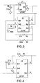
- Figure 3 is a schematic circuit diagram illustrating one embodiment of a circuit having a voltage regulation circuit.
- Figure 4 is a schematic circuit diagram showing one embodiment of a circuit schematic for the RC time-based oscillator unit.
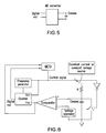
- Figure 5 is a schematic circuit diagram showing a variable capacitor and an IC that is configured to convert capacitance to a digital signal are utilized to form a digital sensor with a transducing capacitor.
- Figure 6 is a schematic circuit diagram showing an MCU controlling the timing of the rest of the circuit.
- the MCU can provide the control signal for the transducing A-to-D converting unit, can store the measured data into local memory, and can deliver modulated data for transmission to the interrogator.
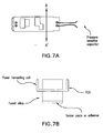
- Figures 7(a) and 7(b) illustrate one embodiment of a PCB-based sensor circuit encapsulated by a fused silica housing.
- FIG 8 is a schematic circuit diagram of an exemplary embodiment of a wireless sensor showing a coil (L1) that is an energy harvesting coil and a capacitor (C10) or a resistor (R5) that varies predictably with the measured physical property.
- a coil (L2) serves as a transmitting coil and a resistor (R1) acts as an attenuator.
- Figure 9 depicts a schematic circuit diagram for an exemplary embodiment of a wireless sensor that uses one coil instead of two.
- Figure 10 depicts the same exemplary circuit as in Figure 9 but with a voltage doubling scheme.
- Figure 11 is a schematic illustration of an exemplary experimental set-up used in one pressure sensing experiment.
- Figure 12 is a graph showing the results of the pressure sensing experiment schematically shown in Figure 11 .
- US 2004/054385 A1 is disclosing a circuit and method for processing the output of an implanted fluorescence sensor which indicates analyte concentration as a function of the fluorescent intensity of a fluorescent indicator.
- the implanted fluorescence sensor is a passive device, and contains no power source.
- the processing circuit powers the sensor through inductively coupled RF energy emitted by the processing circuit.
- the processing circuit receives information from the implanted sensor as variations as in the load on the processing circuit.
- US-A-4 186 749 discloses an induction powered implanted monitor for epidurally measuring intracranial pressure and telemetering the pressure information to a remote readout.
- the monitor utilizes an L-C oscillator in which the C comprises a variable capacitance transducer, one electrode of which is a small stiff pressure responsive diaphragm.
- the oscillator is isolated from a transmitting tank circuit by a buffer circuit and all electric components in the implanted unit except an input and an output coil are shielded by a metal housing.
- WO 00/30534 discloses a biomedical semiconductor integrated circuit device that is spherical in shape for implantation in the biological medium to be monitored or affected.
- the spherical-shaped IC may include transducers to perform a wide variety of instrumentation, monitoring and test or treatment regimes.
- WO 2006/010037 discloses a system for monitoring strain as an indicator of biological conditions, such as spinal fusion, glucose levels, spinal loading, and heart rate.
- the system includes an inter-digitated capacitor sensor, and RF transmitter, and an associated antenna, all of which are microminiature or microscopic in size and can be implanted in a biological host such as a human or animal.
- An inductively coupled power supply is also employed to avoid the need for implantation of chemical batteries. Power is provided to the sensor and transmitter, and data is transmitted from the sensor, when an external receiving device, such as a handheld RF ID type receiver, is placed proximate the location of the implanted sensor, transmitter and inductively coupled power supply.
- Ranges can be expressed herein as from “about” one particular value, and/or to "about” another particular value. When such a range is expressed, another aspect includes from the one particular value and/or to the other particular value. Similarly, when values are expressed as approximations, by use of the antecedent "about,” it will be understood that the particular value forms another aspect. It will be further understood that the endpoints of each of the ranges are significant both in relation to the other endpoint, and independently of the other endpoint.
- the terms "optional” or “optionally” mean that the subsequently described event or circumstance may or may not occur, and that the description includes instances where said event or circumstance occurs and instances where it does not.
- the present invention comprises wireless physical property sensors as defined in the claims incorporating active circuitry and systems incorporating the same.
- the sensors can be integrated with a hermetic, unitary package.
- Active circuitry comprises, e.g., integrated circuits (ICs).
- ICs integrated circuits
- the inclusion of active circuitry in the electrical design of a wireless sensor imparts many new traits. It enables the sensor to sense multiple physical outputs of interest such as, but not limited to, temperature, flow, stress, strain, and chemical properties.
- the addition of active circuitry also decouples the parasitic effects that would otherwise present signal processing challenges, allows for precise compensation or calibration of the sensor and enables some level of real-time statistical computing, averaging, filtering or combination thereof to ensure the statistical fidelity of the information collected by the sensor.
- the active circuitry can be used to manage the power source—be it an on-board temporary (e.g., a capacitor or ultra-capacitor) or a permanent (e.g., a battery) source of energy to operate the sensor in a partially or fully autonomous manner.
- the active circuitry allows for storage of multiple sets of information collected by the sensor or used in processing of the sensor data. Also, the active circuitry enables the storage of personal information relative to the identity of the host and/or the sensor. Furthermore, the active circuitry can enable the use of robust protocols and data transmission techniques to communicate with the interrogator, minimizing the risk of miscommunication and simplifying the interrogator. Sensors ascending to the present invention find widespread use in biomedical, industrial, consumer and automotive applications.
- analog and digital sensors Two distinct types of wireless sensors embodying the characteristics of the prior paragraphs are disclosed herein: analog and digital sensors.
- analog and digital sensors refer to the format of communication between the sensor and the interrogator.
- the analog sensor generates a variable frequency signal whose frequency precisely represents the data to be retrieved.
- the digital sensor digitizes information collected by the sensor prior to transmitting it to the interrogator using some type of binary modulation such as, without limitation, PSK, ASK and FSK.
- the analog wireless sensor is comprised of the following components: a power harvesting unit, an "end of burst" detection unit, a voltage regulation unit, means for delaying energizing the voltage regulation unit until a predetermined time delay has elapsed a transducing oscillator unit, and a transmitting coil.
- a power harvesting unit an "end of burst" detection unit
- a voltage regulation unit means for delaying energizing the voltage regulation unit until a predetermined time delay has elapsed a transducing oscillator unit
- a transmitting coil exemplarily described below.
- the power harvesting unit is comprised of an inductor (L) and a capacitor (C).
- the inductor couples RF magnetic fields and the capacitor forms a resonant circuit when connected with the inductor and rectifying diodes, energy storage capacitors, and over-voltage protection units.
- the number of rectifying diodes used varies according to the geometry of the circuit. At least one rectifying diode for half wave rectification and a plurality of rectifying diodes for full wave rectification are needed. In one non-limiting example, a minimum of one rectifying diode for half wave rectification and four rectifying diodes for full wave rectification can be used.
- a voltage multiplying scheme can be employed, such implementation can involve the addition of a number of diodes and capacitors.
- the energy storage capacitor employs relatively large capacitance value compared to other capacitors in the circuit because it is the only energy source for operation of the wireless sensor in sequential systems. The value can vary from hundreds of pico Farad to tens of microFarad.
- a Zener diode can be used as an over-voltage protection unit.
- FIG. 1 shows one embodiment of a power harvesting unit that employs a voltage doubling scheme.
- the interrogator an generates energizing magnetic field in proximity to the sensor
- the small antenna (Lr) and a capacitor (Cr) pick up the AC voltage in resonance mode. That AC voltage is rectified and charged to a first capacitor C2 through diode D1. Again, the voltage charged in C2 is added to the AC voltage in Lr and Cr, and rectified and charged to capacitor Cs through diode D2.
- the AC voltage available in Lr and Cr is doubled and stored to a second capacitor, Cs, as a DC voltage to be used for sensor operation at a subsequent time.
- a zener diode (Dz) may be incorporated to provide over-voltage protection. This circuit is useful, when the sensor chip used requires high voltage.
- a simple resistive-capacitive (RC) circuit in order to recognize the end of the RF magnetic burst around the sensor, can be used.
- the capacitor of the RC circuit remains charged while RF field is present.
- the capacitor of the RC circuit discharges through the resistor of the RC circuit with a predetermined time delay.
- the time delay is programmed such that energizing RF magnetic field has decayed to a given threshold level.
- the rest of the circuit "wakes up" for data transmission- i.e ., the discharge of the capacitor triggers a switch to connect the rest of the circuit to the energy storage capacitor.
- Figure 2 depicts one embodiment of a circuit comprising a power harvesting unit and an end of burst detection unit.
- the interrogator When the interrogator generates an energizing magnetic field in proximity to the sensor, the electrical energy (i.e., voltage) is harvested and stored to capacitor C2.
- transistor switch QP is open, so that the energy being stored is not available to the main sensor circuit and is thus preserved.
- the main sensor circuit will be connected to the #3 node of switch QP later.
- switch QP closes (the #2 and #3 nodes of QP are electrically connected), and the voltage in C2 is available to power the sensor.
- the L1 and C3 pick up the AC voltage which is doubled and rectified to C2 through C6 and two diodes in BAS40BRW (#1 and #5 node in BAS40BRW). Simultaneously, the AC voltage in L1 and C3 is doubled and rectified to C11 through C7 and two diodes in BAS40BRW (#2 and #4 node in BAS40BRW). Due to the voltage in C11, the switch QP is open and the energy in C3 is not available to the #3 node of switch QP.
- the voltage in C11 dissipates through resistor R and becomes zero in short time (i.e., less than a millisecond). As soon as the voltage in C11 becomes zero, the switch QP closes and the voltage in C2 is available to main sensor circuit.
- the power harvesting unit is a LC-tank that is followed by a rectification stage and an optional voltage multiplication stage. It is then a energy storage stage, such as a capacitor with a desired energy storage space.
- FIG. 3 illustrates one embodiment of a circuit having a voltage regulation circuit.
- the unit V1 is a voltage reference and U2 is an under-voltage lockout unit.
- C8 is noise reduction capacitor.
- the #1 node of V1 is connected to #3 node of QP switch, therefore the voltage stored in C2 is available to the #1 node of V1.
- V1 functions to output a preset voltage level whenever the input (#1) voltage is higher than preset output voltage. This ensures the voltage available to sensor transducer unit is substantially constant
- the sensor transducer unit is connected to output (#2) of V1. The constant level of voltage contributes to the accurate functioning of the transducer unit.
- U2 monitors voltage in C8 and, if the voltage in C8 is smaller than preset voltage, it generates a warning or disabling signal through #6 node of U2.
- the preset voltage level is adjusted with resistor values in R2, R4, and R6. When the voltage is higher than the preset voltage, then the preset voltage is available to #6 node of U2. When the voltage in C8 is lower than the preset voltage, the zero voltage is available to #6 node of U2, either warning or disabling transducer unit.
- the transducing oscillator unit converts physical properties such as, but not limited to, pressure, temperature, stress and the like to electrical signals.
- the electrical signals set the electrical oscillation frequency, which is transmitted to the interrogator. This electrical frequency can be measured and correlated to the value of the measured physical property by the interrogator.
- the RC time constant-based oscillator can be used for setting the electrical oscillation frequency.
- One example is a 555 timer.
- Figure 4 shows one embodiment of a circuit schematic for the RC time-based oscillator unit.
- a capacitor (C10) or a resistor (R5) represents the sensing capacitor or sensing resistor.
- the #4 node is an operating-voltage supply line
- #3 node is a chip-function enabling line.
- the line that is in communication with the #3 node can also be electrically coupled to the #6 node of U2 in the Figure 3 , which acts to shut down the chip when the voltage is lower than the preset voltage.
- the exemplary circuit is configured such that the oscillator frequency can be varied by the value of C10 and R5 and can be available through the #5 node in order to be transmitted back to the reader or interrogator wirelessly.
- a passive (no battery) LC resonant circuit is composed of two electrical passive components that are connected in series: a coil or inductor ("L"), and a capacitor ("C").
- L coil or inductor
- C capacitor
- Such a passive electrical circuit exhibits electrical resonance when subjected to an alternating electromagnetic field.
- the electrical resonance is particularly acute for a specific frequency value or range of the impinging signal.
- the impinging signal substantially reaches the resonant frequency of the LC resonant circuit inside the sensor assembly, a pronounced disturbance of the field can be detected wirelessly.
- the electrical resonance occurs for a frequency f, related to the value of L and C according to equation 1 above.
- the passive electrical resonant circuit for the assemblies described herein that utilize a passive electrical resonant circuit can be fabricated via conventional MEMS approach to sensor design, which lends itself to the fabrication of small sensors that can be formed using biocompatible polymers as substrate materials.
- appropriately biocompatible coatings can be applied to the surfaces of the respective assemblies in order to prevent adhesion of biological substances to the respective assemblies that could interfere with their proper function.
- the passive electrical resonant circuit of the assembly can be manufactured using Micro-machining techniques that were developed for the integrated circuit industry.
- An example of this type of sensor features an inductive-capacitive (LC) resonant circuit with a variable capacitor is described in Allen et al., U.S. Pat. No. 6,111,520 .
- LC inductive-capacitive
- the capacitance varies with the pressure of the environment in which the capacitor is placed. Consequently, the resonant frequency of the exemplary LC circuit of the Allen pressure sensor varies depending on the pressure of the environment.
- piezoresistive material can be used to transduce sensed stress to resistance.
- An example of this type of sensor is exemplarily described in Gershenfeld et al., U.S. Pat. No. 6,025,725 .
- a thermistor to convert temperature to resistance, can be employed.
- the thermistor is defined as a metal whose specific electrical resistance varies according to the temperature of a material.
- the environmental temperature determines the resistance which, in turn, determines the oscillation frequency of the RC oscillator unit.
- the thermistor is attached to the sensor housing for better thermal conduction.
- the senor can be configured to convert a sensed physical property into an electrical signal comprises.
- this conversion can comprise converting sensed temperature changes to resistance changes via a temperature sensitive resistor.
- this conversion can comprise converting sensed changes in pressure to changes in capacitance values via a pressure sensitive capacitor.
- this conversion can comprise converting sensed stress changes to resistance changes via a stress sensitive resistor.
- a voltage controlled oscillator can also be used for transducing a physical property of interest to an electrical signal.
- VCO voltage controlled oscillator
- a conventional VCO is an electronic circuit whose electrical oscillation output is a function of the voltage applied.
- the measured physical property is converted to a voltage that determines the broadcasting electrical frequency.
- Many physical properties are readily converted to voltage.
- such convertible physical properties include measured temperature, stress, pressure or the like.
- a constant current source can be applied to a resistor.
- the induced voltage at the end of the resistor is proportional to the value of the resistor. Therefore, temperature change can be converted to voltage through a thermistor.
- piezoresitors can be arranged into a Wheatstone bridge configuration, which is configured to achieve a higher voltage sensitivity while geometrically compensating for temperature effects.
- the stress applied by the external environment to the deformable region of the sensor determines the output voltage of the Wheatstone bridge, and which sets the electrical oscillation for broadcasting.
- an identification signal or signature can be added to the transmitted signal.
- the oscillation frequency can be amplitude modulated prior to transmission to the interrogator.
- the interrogator can confirm this signature and authenticate that the frequency is coming from a specific wireless sensor or merely the wireless sensor at all. This signature modality allows for sensor identification and avoids any confusion with other resonances present in the environment.
- a digital wireless sensor is comprised of the following components: a power harvesting unit, an end of burst detection unit, a microcontroller unit (MCU), a transducing analog-to-digital converter unit, a transmitting coil.
- a voltage regulation unit incorporated into the digital wireless sensor, and means for delaying energizing the voltage regulation unit until a predetermined time delay has elapsed.
- the design of the power harvesting unit, the end of burst detection unit and the voltage regulation unit are substantially the same for the digital sensor as described above for the analog sensor.
- a variable capacitor and an IC that is configured to convert capacitance to a digital signal are utilized to form a digital sensor with a transducing capacitor.
- the MCU sends out a signal to start the frequency generator and the counter. Substantially simultaneously, the capacitance is charged at a controlled rate.
- a constant current source or a constant voltage source can be used to charge the capacitor.
- the constant current source does not require a resistor can also produce a more linear digital output over a wide range of capacitance.
- the comparator trips and the counter is turned off.
- the MCU reads the digital output and discharges the capacitor in preparation for the next measurement.
- the digital output is a number that is substantially proportional to the capacitance value.
- the-digital output resolution depends on the frequency of the frequency generator, which should be kept high enough to support resolution of the capacitance value necessary for meaningful output to the end user of the system.
- the MCU controls the timing of the rest of the circuit.
- the MCU can provide the control signal for the transducing A-to-D converting unit, can store the measured data into local memory, and can deliver modulated data for transmission to the interrogator.
- Conventional off-the-shelf MCU chips typically comprise a frequency generator, a counter, and a comparator with voltage references, and can realize the schematic in Figure 6 with minimal components added.
- FIG 8 shows a schematic circuit diagram of an exemplary embodiment of a wireless sensor.
- a coil (L1) is an energy harvesting coil and a capacitor (C10) or a resistor (R5) varies predictably with the measured physical property.
- a coil (L2) serves as a transmitting coil and a resistor (R1) acts as an attenuator.
- Figure 9 depicts a schematic for an exemplary embodiment of a wireless sensor that uses one coil instead of two.
- the plurality of inductor coils employed in the previous examples are not functionally active simultaneously, i.e., the transmit coil is not in use while the energy pick up coil is active and vice-versa. Therefore, a single coil wireless sensor is achievable with certain modifications.
- the output of the transducer oscillator can be connected to the coil (L1) through MOSFET switch M3 whenever the transducer oscillator activates and transmits a signal.
- coil L1 can be used for both energy harvesting and signal transmission.
- Figure 10 depicts the same circuit as in Figure 9 but with a voltage doubling scheme.
- the packaging of the sensors can comprise encapsulating PCB-based sensor circuits in ceramic housings.
- the ceramic housing can be completed either via laser fusion, anodic bonding or eutectic bonding.
- the PCB-based sensor circuit can be replaced with an ASIC and this replacement is within the scope of the present invention.
- the sensor can be packaged by the methods disclosed in US Patent Application Serial No. 11/472,905, filed June 22, 2006 ; US Patent Application Serial No. 11/314,046, filed December 20, 2005 ; US Patent Application Serial No. 11/157,375, filed June 21, 2005 .
- Figures 7(a) and 7(b) illustrate one possible embodiment of a PCB-based sensor circuit encapsulated by a fused silica housing.
- the external source of the energizing magnetic field such as an interrogator
- the external source will transmit energy at a substantially constant preselected frequency.
- the external source will activate or energize for a predetermined period of time, during which time the power harvesting unit of the wireless sensor is energized.
- energy accumulated in the power harvesting unit is supplied to the voltage regulation unit and is subsequently supplied to the transducing oscillator unit at the substantially constant preset voltage level output from the voltage regulation unit.
- the electrical signal indicative of the sensed physical property is transmitted via the transmitting coil of the sensor to a remote, external antenna, which can form a portion of the interrogator.
- FIG 11 shows the brief illustration of an exemplary experimental set-up used in one pressure sensing experiment.
- the capacitor (C10) in the schematic illustrated in Figure 8 is replaced with a pressure sensitive capacitor. Pressure was applied to the sensor via a hand pump.
- the timing control unit sent out periodic triggering (on/off) signal to RF power amp.
- a strong 13.56MHz signal was turned on/off at a rate of 35Hz and subsequently feed to the antenna.
- the wireless pressure sensor "wakes up” and transmits the pressure information in the form of electrical frequency.
- a receiving antenna sensed the transmitted frequency by wireless sensor, and then the received signal was amplified and feed to the frequency counter. The results of the experiment are shown in Figure 12 .
Landscapes
- Engineering & Computer Science (AREA)
- Health & Medical Sciences (AREA)
- Life Sciences & Earth Sciences (AREA)
- Physics & Mathematics (AREA)
- Computer Networks & Wireless Communication (AREA)
- Power Engineering (AREA)
- General Physics & Mathematics (AREA)
- Heart & Thoracic Surgery (AREA)
- Pathology (AREA)
- Biomedical Technology (AREA)
- Biophysics (AREA)
- Medical Informatics (AREA)
- Molecular Biology (AREA)
- Surgery (AREA)
- Animal Behavior & Ethology (AREA)
- General Health & Medical Sciences (AREA)
- Public Health (AREA)
- Veterinary Medicine (AREA)
- Arrangements For Transmission Of Measured Signals (AREA)
- Measuring Fluid Pressure (AREA)
Claims (15)
- Implantierbarer drahtloser Sensor, der
eine Energiegewinnungseinheit;
eine Spannungsregeleinheit, die elektrisch mit der Energiegewinnungseinheit gekoppelt ist, wobei die Spannungsregeleinheit eingerichtet ist, um bei einem minimalen Spannungspegel auszulösen;
eine signalübertragende Oszillatoreinheit, die elektrisch mit der Spannungsregeleinheit gekoppelt ist, wobei die signalübertragende Oszillatoreinheit ein Mittel zur Umwandlung einer erfassten physikalischen Eigenschaft in ein elektrisches Signal aufweist; und
eine Sendespule aufweist, die eingerichtet ist, das elektrische Signal zu empfangen und das elektrische Signal an eine externe Antenne zu übertragen, dadurch gekennzeichnet, dass sie ferner Mittel zum Verzögern der Energielieferung an die Spannungsregeleinheit bis eine vorbestimmte Zeitverzögerung verstrichen ist, aufweist. - Implantierbarer drahtloser Sensor nach Anspruch 1, wobei das Mittel zum Verzögern der Energielieferung mit der Energiegewinnungseinheit und der Spannungsregeleinheit gekoppelt ist.
- Implantierbarer drahtloser Sensor nach Anspruch 2, wobei das Mittel zum Verzögern der Energielieferung eine Widerstands-Kondensator(RC)-Schaltung aufweist.
- Implantierbarer drahtloser Sensor nach Anspruch 3, wobei die RC-Schaltung eingerichtet ist, um einen Solid-State-Schalter, der zwischen der Energiegewinnungseinheit und der Spannungsregeleinheit angeschlossen ist, zu aktivieren.
- Implantierbarer drahtloser Sensor nach Anspruch 3, wobei die RC-Schaltung einen Kondensator, der mit einem Widerstand gekoppelt ist, aufweist, wobei der Kondensator eingerichtet ist, um Energie während der Anwendung eines externen energieliefernden Magnetfeldes zu speichern und wobei die gespeicherte Energie durch den Widerstand über die vorbestimmte Zeitverzögerung nach Entfernen des externen energieliefernden Magnetfeldes entladen wird.
- Implantierbarer drahtloser Sensor nach Anspruch 1, wobei die Energiegewinnungseinheit eine Antenne aufweist, die eingerichtet ist, um das externe energieliefernde Magnetfeld zu empfangen;
einen ersten mit der Antenne gekoppelten Kondensator aufweist, der eingerichtet ist, um bei einer vorbestimmten Frequenz zu schwingen; und ein Mittel aufweist zum Gleichrichten der in einem zweiten Kondensator zur Verwendung durch den Sensor zu einer nachfolgenden Zeit zu speichernden Spannung. - Implantierbarer drahtloser Sensor nach Anspruch 6, wobei das Mittel zum Gleichrichten der in einem zweiten Kondensator zu speichernden Spannung ferner umfasst, dass die in dem zweiten Kondensator zu speichernde Spannung mindestens verdoppelt wird.
- Implantierbarer drahtloser Sensor nach Anspruch 7, wobei die Energiegewinnungseinheit ferner eine betreibbar mit dem zweiten Kondensator gekoppelte Zenerdiode aufweist.
- Implantierbarer drahtloser Sensor nach Anspruch 1, wobei die Spannungsregeleinheit eine Spannungsreferenzeinheit, die elektrisch mit der Energiegewinnungseinheit gekoppelt ist, wobei die Spannungsreferenzeinheit eingerichtet ist, um einen im Wesentlichen konstanten voreingestellten Spannungspegel auszugeben wenn die von der Energiegewinnungseinheit empfangene Spannung höher ist als die voreingestellte Ausgangsspannung; und eine Unterspannungs-Lockout-Einheit aufweist, die elektrisch mit der Referenzspannungseinheit gekoppelt ist.
- Implantierbarer drahtloser Sensor nach Anspruch 1, wobei die erfasste physikalische Eigenschaft aus einer Gruppe bestehend aus Druck, Belastung, Dehnung, oder Temperatur ausgewählt ist.
- Implantierbarer drahtloser Sensor nach Anspruch 1, wobei das Mittel zum Umwandeln einer erfassten physikalischen Eigenschaft in ein elektrisches Signal Mittel zum Umwandeln erfasster Temperaturänderungen in Widerstandsänderungen aufweist, wobei vorzugsweise das Mittel zum Umwandeln erfasster Temperaturänderungen in Widerstandsänderungen einen temperaturempfindlichen Widerstand aufweist;
oder wobei das Mittel zum Umwandeln einer erfassten physikalischen Eigenschaft in ein elektrisches Signal Mittel zum Umwandeln erfasster Druckänderungen in Änderungen von Kapazitätswerten aufweist, wobei vorzugsweise das Mittel zum Umwandeln erfasster Druckänderungen in Änderungen von Kapazitätswerten einen druckempfindlichen Kondensator aufweist;
oder wobei das Mittel zum Umwandeln einer erfassten physikalischen Eigenschaft in ein elektrisches Signal Mittel zum Umwandeln erfasster Belastungsänderungen in Widerstandsänderungen aufweist, wobei vorzugsweise das Mittel zum Umwandeln erfasster Belastungsänderungen in Widerstandsänderungen einen belastungsempfindlichen Widerstand aufweist. - Implantierbarer drahtloser Sensor nach Anspruch 1, wobei das Mittel zum Umwandeln einer erfassten physikalischen Eigenschaft in ein elektrisches Signal einen spannungsgesteuerten Oszillator aufweist.
- Implantierbarer drahtloser Sensor nach Anspruch 12, wobei der spannungsgesteuerte Oszillator ein Mittel zum Umwandeln der erfassten physikalischen Eigenschaft in eine Spannung aufweist, die die Frequenz der Ausgabe (Output) des spannungsgesteuerten Oszillators bestimmt.
- Implantierbarer drahtloser Sensor nach Anspruch 1, wobei das elektrische Signal ferner ein Kennsignal aufweist, das einzigartig für jeden Sensor ist.
- Implantierbarer drahtloser Sensor nach Anspruch 1, wobei die Energiegewinnungseinheit ein LC-Schwingkreis ist.
Applications Claiming Priority (2)
| Application Number | Priority Date | Filing Date | Title |
|---|---|---|---|
| US8220708P | 2008-07-20 | 2008-07-20 | |
| PCT/US2009/051177 WO2010011612A1 (en) | 2008-07-20 | 2009-07-20 | Physical property sensor with active electronic circuit and wireless power and data transmission |
Publications (2)
| Publication Number | Publication Date |
|---|---|
| EP2330968A1 EP2330968A1 (de) | 2011-06-15 |
| EP2330968B1 true EP2330968B1 (de) | 2013-04-03 |
Family
ID=41165376
Family Applications (1)
| Application Number | Title | Priority Date | Filing Date |
|---|---|---|---|
| EP09790645A Active EP2330968B1 (de) | 2008-07-20 | 2009-07-20 | Sensor zur messung physikalischer eigenschaften mit aktivem elektronischem kreislauf und drahtloser strom- und datenübertragung |
Country Status (5)
| Country | Link |
|---|---|
| US (3) | US8264240B2 (de) |
| EP (1) | EP2330968B1 (de) |
| AU (1) | AU2009274140B2 (de) |
| CA (1) | CA2731251C (de) |
| WO (1) | WO2010011612A1 (de) |
Cited By (12)
| Publication number | Priority date | Publication date | Assignee | Title |
|---|---|---|---|---|
| US9384607B1 (en) | 2014-12-03 | 2016-07-05 | Tyco Fire & Security Gmbh | Access control system |
| US10806428B2 (en) | 2015-02-12 | 2020-10-20 | Foundry Innovation & Research 1, Ltd. | Implantable devices and related methods for heart failure monitoring |
| US10806352B2 (en) | 2016-11-29 | 2020-10-20 | Foundry Innovation & Research 1, Ltd. | Wireless vascular monitoring implants |
| CN112729624A (zh) * | 2020-12-04 | 2021-04-30 | 厦门大学 | 一种阵列式lc压力传感器集成装置 |
| US11039813B2 (en) | 2015-08-03 | 2021-06-22 | Foundry Innovation & Research 1, Ltd. | Devices and methods for measurement of Vena Cava dimensions, pressure and oxygen saturation |
| US11206992B2 (en) | 2016-08-11 | 2021-12-28 | Foundry Innovation & Research 1, Ltd. | Wireless resonant circuit and variable inductance vascular monitoring implants and anchoring structures therefore |
| US11564596B2 (en) | 2016-08-11 | 2023-01-31 | Foundry Innovation & Research 1, Ltd. | Systems and methods for patient fluid management |
| US11701018B2 (en) | 2016-08-11 | 2023-07-18 | Foundry Innovation & Research 1, Ltd. | Wireless resonant circuit and variable inductance vascular monitoring implants and anchoring structures therefore |
| US11779238B2 (en) | 2017-05-31 | 2023-10-10 | Foundry Innovation & Research 1, Ltd. | Implantable sensors for vascular monitoring |
| US11944495B2 (en) | 2017-05-31 | 2024-04-02 | Foundry Innovation & Research 1, Ltd. | Implantable ultrasonic vascular sensor |
| US12465233B2 (en) | 2022-07-29 | 2025-11-11 | Foundry Innovation & Research 1, Ltd. | Multistranded conductors adapted to dynamic in vivo environments |
| US12465324B2 (en) | 2015-02-12 | 2025-11-11 | Foundry Innovation & Research 1, Ltd. | Patient fluid management systems and methods employing integrated fluid status sensing |
Families Citing this family (36)
| Publication number | Priority date | Publication date | Assignee | Title |
|---|---|---|---|---|
| JP2011159767A (ja) * | 2010-01-29 | 2011-08-18 | Toshiba Corp | Ledパッケージ及びその製造方法 |
| US8400744B2 (en) * | 2010-05-19 | 2013-03-19 | Schneider Electric USA, Inc. | Earth leakage detection module with robust transient suppression |
| EP2400308A1 (de) * | 2010-06-10 | 2011-12-28 | ABB Technology AG | Drahtlose Strommessvorrichtung |
| US9435819B1 (en) * | 2012-04-27 | 2016-09-06 | Cree Fayetteville, Inc. | Autonomous temperature accelerometer sensor |
| HK1210524A1 (en) | 2012-07-25 | 2016-04-22 | California Institute Of Technology | Nanopillar field-effect and junction transistors with functionalized gate and base electrodes |
| AU2013332347A1 (en) * | 2012-10-16 | 2015-04-09 | California Institute Of Technology | Systems and methods for wireless transducers through integrated on-chip antenna |
| US8883645B2 (en) | 2012-11-09 | 2014-11-11 | California Institute Of Technology | Nanopillar field-effect and junction transistors |
| US9385560B2 (en) | 2013-11-12 | 2016-07-05 | Qualcomm Incorporated | Methods, devices and systems for self charging sensors |
| GB2540565B (en) * | 2015-07-21 | 2019-04-24 | Skf Ab | Sensor assembly for bearing with wireless temperature sensor |
| CN114532976A (zh) | 2016-05-31 | 2022-05-27 | 酷拉公司 | 可植入眼压传感器和使用方法 |
| WO2018158640A1 (en) * | 2017-03-02 | 2018-09-07 | Awesense Wireless Inc. | Selectable power scavenging systems and methods |
| US9961749B1 (en) * | 2017-04-12 | 2018-05-01 | Climax Technology Co., Ltd. | RF controlled switch box without using neutral wire and a power harvesting switch circuit thereof |
| WO2019032488A1 (en) | 2017-08-07 | 2019-02-14 | DePuy Synthes Products, Inc. | IMPLANTABLE SENSORS IN THE BODY OF A PATIENT, SYSTEMS AND METHODS OF USING THE SAME |
| US11330981B2 (en) | 2018-12-20 | 2022-05-17 | Pacesetter, Inc. | Method and apparatus for a burst operation pressure sensor |
| US11990763B2 (en) * | 2019-02-18 | 2024-05-21 | Ibbx Inovação Em Sistemas De Software E Hardware Ltda | Resonance generator system and method for capturing oscillatory signals |
| EP3906841A1 (de) | 2020-05-08 | 2021-11-10 | Pacesetter, Inc. | Verfahren und system zur erfassung des herzzustandes mittels eines beschleunigungsmessers |
| US20210345891A1 (en) | 2020-05-08 | 2021-11-11 | Pacesetter, Inc. | Method and device for detecting respiration anomaly from low frequency component of electrical cardiac activity signals |
| US12514505B2 (en) | 2020-08-31 | 2026-01-06 | DePuy Synthes Products, Inc. | Hermetic enclosure for implantable sensors |
| US20220320900A1 (en) * | 2021-04-05 | 2022-10-06 | Baker Hughes Oilfield Operations Llc | Sensing system and associated components and methods |
| EP4088662B1 (de) | 2021-05-13 | 2024-08-07 | Pacesetter, Inc. | Verfahren und system zur überwachung der herzfunktion basierend auf dem herztonmassenschwerpunkt |
| CN117882321A (zh) | 2021-06-29 | 2024-04-12 | 优林克实验室公司 | 用于在异质介质中建立无线链路的系统、装置和方法 |
| US11931587B2 (en) | 2021-07-06 | 2024-03-19 | Pacesetter, Inc. | Method and system for implanting a septal wall electrode |
| US20230109023A1 (en) * | 2021-10-05 | 2023-04-06 | Tc1 Llc | System and method for intra-body communication of sensed physiologic data |
| WO2024073322A2 (en) | 2022-09-30 | 2024-04-04 | Tc1 Llc | Tandem interlace delivery catheter for delivering an intracorporeal sensor |
| WO2024144872A1 (en) | 2022-12-28 | 2024-07-04 | Pacesetter, Inc. | Method and system for implanting a septal wall electrode |
| WO2024172917A1 (en) | 2023-02-14 | 2024-08-22 | Tc1 Llc | Implantable pressure sensor drift detection |
| WO2024263311A1 (en) | 2023-06-20 | 2024-12-26 | Tc1 Llc | Sensor anchor loop configurations for lodging an implantable wireless sensor in a lumen |
| US20240424307A1 (en) | 2023-06-22 | 2024-12-26 | Pacesetter, Inc. | Method and system for monitoring heart function based on electromechanical activation time |
| WO2025101366A1 (en) | 2023-11-06 | 2025-05-15 | Tc1 Llc | System and method for diastolic-enhanced systolic peak detection |
| WO2025136641A1 (en) | 2023-12-20 | 2025-06-26 | Tc1 Llc | Implantable sensor signal lock through single ping transmission |
| WO2025136783A1 (en) | 2023-12-21 | 2025-06-26 | Tc1 Llc | Methods and systems for displaying healthcare metrics associated with patient populations |
| WO2025136640A1 (en) | 2023-12-22 | 2025-06-26 | Tc1 Llc | Systems and methods for wavelet transformation based dicrotic notch extraction and arrhythmia detection |
| WO2025212628A1 (en) | 2024-04-04 | 2025-10-09 | Tc1 Llc | Method and device for cardiac pressure sensing using an active implantable device and near field communication |
| US20250375156A1 (en) | 2024-06-05 | 2025-12-11 | Pacesetter, Inc. | Methods and systems for heart health diagnostics |
| CN118470945A (zh) * | 2024-07-10 | 2024-08-09 | 壹甲子(成都)通讯有限公司 | 一种高速高分辨的无线传感方法及系统 |
| US20260053460A1 (en) | 2024-08-22 | 2026-02-26 | Pacesetter, Inc. | Methods and systems for using seismocardiography-based algorithm for monitoring heart valve operation |
Family Cites Families (8)
| Publication number | Priority date | Publication date | Assignee | Title |
|---|---|---|---|---|
| US4186749A (en) | 1977-05-12 | 1980-02-05 | The United States Of America As Represented By The Administrator Of The National Aeronautics And Space Administration | Induction powered biological radiosonde |
| WO2000030534A1 (en) | 1998-11-25 | 2000-06-02 | Ball Semiconductor, Inc. | Spherically-shaped biomedical ic |
| US7553280B2 (en) | 2000-06-29 | 2009-06-30 | Sensors For Medicine And Science, Inc. | Implanted sensor processing system and method |
| US7081693B2 (en) * | 2002-03-07 | 2006-07-25 | Microstrain, Inc. | Energy harvesting for wireless sensor operation and data transmission |
| WO2006010037A2 (en) * | 2004-07-08 | 2006-01-26 | Deborah Schenberger | Strain monitoring system and apparatus |
| US7276703B2 (en) * | 2005-11-23 | 2007-10-02 | Lockheed Martin Corporation | System to monitor the health of a structure, sensor nodes, program product, and related methods |
| US8744544B2 (en) * | 2007-10-17 | 2014-06-03 | Integrated Sensing Systems, Inc. | System having wireless implantable sensor |
| CA2777596C (en) * | 2009-10-13 | 2018-05-29 | Cynetic Designs Ltd. | An inductively coupled power and data transmission system |
-
2009
- 2009-07-20 WO PCT/US2009/051177 patent/WO2010011612A1/en not_active Ceased
- 2009-07-20 AU AU2009274140A patent/AU2009274140B2/en active Active
- 2009-07-20 EP EP09790645A patent/EP2330968B1/de active Active
- 2009-07-20 CA CA2731251A patent/CA2731251C/en active Active
- 2009-07-20 US US12/506,170 patent/US8264240B2/en active Active
-
2012
- 2012-08-17 US US13/588,518 patent/US9041416B2/en active Active
-
2015
- 2015-05-21 US US14/718,743 patent/US9653926B2/en active Active
Cited By (16)
| Publication number | Priority date | Publication date | Assignee | Title |
|---|---|---|---|---|
| US9384607B1 (en) | 2014-12-03 | 2016-07-05 | Tyco Fire & Security Gmbh | Access control system |
| US10806428B2 (en) | 2015-02-12 | 2020-10-20 | Foundry Innovation & Research 1, Ltd. | Implantable devices and related methods for heart failure monitoring |
| US12465324B2 (en) | 2015-02-12 | 2025-11-11 | Foundry Innovation & Research 1, Ltd. | Patient fluid management systems and methods employing integrated fluid status sensing |
| US10905393B2 (en) | 2015-02-12 | 2021-02-02 | Foundry Innovation & Research 1, Ltd. | Implantable devices and related methods for heart failure monitoring |
| US11039813B2 (en) | 2015-08-03 | 2021-06-22 | Foundry Innovation & Research 1, Ltd. | Devices and methods for measurement of Vena Cava dimensions, pressure and oxygen saturation |
| US12268493B2 (en) | 2016-08-11 | 2025-04-08 | Foundry Innovation & Research 1, Ltd. | Systems and methods for self-directed patient fluid management |
| US11206992B2 (en) | 2016-08-11 | 2021-12-28 | Foundry Innovation & Research 1, Ltd. | Wireless resonant circuit and variable inductance vascular monitoring implants and anchoring structures therefore |
| US11564596B2 (en) | 2016-08-11 | 2023-01-31 | Foundry Innovation & Research 1, Ltd. | Systems and methods for patient fluid management |
| US11701018B2 (en) | 2016-08-11 | 2023-07-18 | Foundry Innovation & Research 1, Ltd. | Wireless resonant circuit and variable inductance vascular monitoring implants and anchoring structures therefore |
| US12310707B2 (en) | 2016-08-11 | 2025-05-27 | Foundry Innovation & Research 1, Ltd. | Wireless resonant circuit and variable inductance vascular monitoring implants and anchoring structures therefore |
| US10806352B2 (en) | 2016-11-29 | 2020-10-20 | Foundry Innovation & Research 1, Ltd. | Wireless vascular monitoring implants |
| US11779238B2 (en) | 2017-05-31 | 2023-10-10 | Foundry Innovation & Research 1, Ltd. | Implantable sensors for vascular monitoring |
| US11944495B2 (en) | 2017-05-31 | 2024-04-02 | Foundry Innovation & Research 1, Ltd. | Implantable ultrasonic vascular sensor |
| CN112729624B (zh) * | 2020-12-04 | 2021-10-15 | 厦门大学 | 一种阵列式lc压力传感器集成装置 |
| CN112729624A (zh) * | 2020-12-04 | 2021-04-30 | 厦门大学 | 一种阵列式lc压力传感器集成装置 |
| US12465233B2 (en) | 2022-07-29 | 2025-11-11 | Foundry Innovation & Research 1, Ltd. | Multistranded conductors adapted to dynamic in vivo environments |
Also Published As
| Publication number | Publication date |
|---|---|
| AU2009274140B2 (en) | 2014-10-16 |
| US20100019778A1 (en) | 2010-01-28 |
| US8264240B2 (en) | 2012-09-11 |
| US9041416B2 (en) | 2015-05-26 |
| WO2010011612A1 (en) | 2010-01-28 |
| US9653926B2 (en) | 2017-05-16 |
| US20120313649A1 (en) | 2012-12-13 |
| CA2731251A1 (en) | 2010-01-28 |
| CA2731251C (en) | 2017-05-30 |
| US20150255995A1 (en) | 2015-09-10 |
| AU2009274140A1 (en) | 2010-01-28 |
| EP2330968A1 (de) | 2011-06-15 |
Similar Documents
| Publication | Publication Date | Title |
|---|---|---|
| EP2330968B1 (de) | Sensor zur messung physikalischer eigenschaften mit aktivem elektronischem kreislauf und drahtloser strom- und datenübertragung | |
| Stangel et al. | A programmable intraocular CMOS pressure sensor system implant | |
| US6433629B2 (en) | Micropower differential sensor measurement | |
| US7236092B1 (en) | Passive sensor technology incorporating energy storage mechanism | |
| US7170201B2 (en) | Energy harvesting for wireless sensor operation and data transmission | |
| CN110770754B (zh) | 能量收集rfid电路、能量收集rfid标签及相关方法 | |
| KR100988671B1 (ko) | 타이어 압력 검지 시스템 및 타이어 압력 검지 장치 | |
| US7256695B2 (en) | Remotely powered and remotely interrogated wireless digital sensor telemetry system | |
| KR102071396B1 (ko) | 측정 센서 | |
| TW201412047A (zh) | 測量無線感測中之可變阻抗元件的系統與方法 | |
| Kaiser | Passive telemetric readout system | |
| DeHennis et al. | A passive-telemetry-based pressure sensing system | |
| JP4827832B2 (ja) | タイヤ圧力検知システム及びタイヤ圧力検知装置 | |
| CN100586744C (zh) | 轮胎压力检测装置 | |
| Lin et al. | A high gauge factor capacitive strain sensor and its telemetry application in biomechanics | |
| Vernooy et al. | Remote excitation and readout of a high Q silicon resonator | |
| HK1203461B (en) | A measurement sensor |
Legal Events
| Date | Code | Title | Description |
|---|---|---|---|
| PUAI | Public reference made under article 153(3) epc to a published international application that has entered the european phase |
Free format text: ORIGINAL CODE: 0009012 |
|
| 17P | Request for examination filed |
Effective date: 20110215 |
|
| AK | Designated contracting states |
Kind code of ref document: A1 Designated state(s): AT BE BG CH CY CZ DE DK EE ES FI FR GB GR HR HU IE IS IT LI LT LU LV MC MK MT NL NO PL PT RO SE SI SK SM TR |
|
| AX | Request for extension of the european patent |
Extension state: AL BA RS |
|
| 17Q | First examination report despatched |
Effective date: 20110916 |
|
| DAX | Request for extension of the european patent (deleted) | ||
| RIN1 | Information on inventor provided before grant (corrected) |
Inventor name: CROS, FLORENT Inventor name: ALLEN, MARK Inventor name: PARK, JIN-WOO |
|
| RIC1 | Information provided on ipc code assigned before grant |
Ipc: A61B 5/00 20060101AFI20120807BHEP Ipc: H02J 7/02 20060101ALI20120807BHEP |
|
| GRAP | Despatch of communication of intention to grant a patent |
Free format text: ORIGINAL CODE: EPIDOSNIGR1 |
|
| GRAS | Grant fee paid |
Free format text: ORIGINAL CODE: EPIDOSNIGR3 |
|
| GRAA | (expected) grant |
Free format text: ORIGINAL CODE: 0009210 |
|
| AK | Designated contracting states |
Kind code of ref document: B1 Designated state(s): AT BE BG CH CY CZ DE DK EE ES FI FR GB GR HR HU IE IS IT LI LT LU LV MC MK MT NL NO PL PT RO SE SI SK SM TR |
|
| REG | Reference to a national code |
Ref country code: GB Ref legal event code: FG4D |
|
| REG | Reference to a national code |
Ref country code: AT Ref legal event code: REF Ref document number: 604186 Country of ref document: AT Kind code of ref document: T Effective date: 20130415 Ref country code: CH Ref legal event code: EP |
|
| REG | Reference to a national code |
Ref country code: IE Ref legal event code: FG4D |
|
| REG | Reference to a national code |
Ref country code: DE Ref legal event code: R096 Ref document number: 602009014731 Country of ref document: DE Effective date: 20130606 |
|
| REG | Reference to a national code |
Ref country code: AT Ref legal event code: MK05 Ref document number: 604186 Country of ref document: AT Kind code of ref document: T Effective date: 20130403 |
|
| PG25 | Lapsed in a contracting state [announced via postgrant information from national office to epo] |
Ref country code: SI Free format text: LAPSE BECAUSE OF FAILURE TO SUBMIT A TRANSLATION OF THE DESCRIPTION OR TO PAY THE FEE WITHIN THE PRESCRIBED TIME-LIMIT Effective date: 20130403 |
|
| REG | Reference to a national code |
Ref country code: NL Ref legal event code: VDEP Effective date: 20130403 |
|
| REG | Reference to a national code |
Ref country code: LT Ref legal event code: MG4D |
|
| PG25 | Lapsed in a contracting state [announced via postgrant information from national office to epo] |
Ref country code: SE Free format text: LAPSE BECAUSE OF FAILURE TO SUBMIT A TRANSLATION OF THE DESCRIPTION OR TO PAY THE FEE WITHIN THE PRESCRIBED TIME-LIMIT Effective date: 20130403 Ref country code: ES Free format text: LAPSE BECAUSE OF FAILURE TO SUBMIT A TRANSLATION OF THE DESCRIPTION OR TO PAY THE FEE WITHIN THE PRESCRIBED TIME-LIMIT Effective date: 20130714 Ref country code: FI Free format text: LAPSE BECAUSE OF FAILURE TO SUBMIT A TRANSLATION OF THE DESCRIPTION OR TO PAY THE FEE WITHIN THE PRESCRIBED TIME-LIMIT Effective date: 20130403 Ref country code: AT Free format text: LAPSE BECAUSE OF FAILURE TO SUBMIT A TRANSLATION OF THE DESCRIPTION OR TO PAY THE FEE WITHIN THE PRESCRIBED TIME-LIMIT Effective date: 20130403 Ref country code: NL Free format text: LAPSE BECAUSE OF FAILURE TO SUBMIT A TRANSLATION OF THE DESCRIPTION OR TO PAY THE FEE WITHIN THE PRESCRIBED TIME-LIMIT Effective date: 20130403 Ref country code: BE Free format text: LAPSE BECAUSE OF FAILURE TO SUBMIT A TRANSLATION OF THE DESCRIPTION OR TO PAY THE FEE WITHIN THE PRESCRIBED TIME-LIMIT Effective date: 20130403 Ref country code: PT Free format text: LAPSE BECAUSE OF FAILURE TO SUBMIT A TRANSLATION OF THE DESCRIPTION OR TO PAY THE FEE WITHIN THE PRESCRIBED TIME-LIMIT Effective date: 20130805 Ref country code: LT Free format text: LAPSE BECAUSE OF FAILURE TO SUBMIT A TRANSLATION OF THE DESCRIPTION OR TO PAY THE FEE WITHIN THE PRESCRIBED TIME-LIMIT Effective date: 20130403 Ref country code: GR Free format text: LAPSE BECAUSE OF FAILURE TO SUBMIT A TRANSLATION OF THE DESCRIPTION OR TO PAY THE FEE WITHIN THE PRESCRIBED TIME-LIMIT Effective date: 20130704 Ref country code: NO Free format text: LAPSE BECAUSE OF FAILURE TO SUBMIT A TRANSLATION OF THE DESCRIPTION OR TO PAY THE FEE WITHIN THE PRESCRIBED TIME-LIMIT Effective date: 20130703 Ref country code: IS Free format text: LAPSE BECAUSE OF FAILURE TO SUBMIT A TRANSLATION OF THE DESCRIPTION OR TO PAY THE FEE WITHIN THE PRESCRIBED TIME-LIMIT Effective date: 20130803 |
|
| PG25 | Lapsed in a contracting state [announced via postgrant information from national office to epo] |
Ref country code: BG Free format text: LAPSE BECAUSE OF FAILURE TO SUBMIT A TRANSLATION OF THE DESCRIPTION OR TO PAY THE FEE WITHIN THE PRESCRIBED TIME-LIMIT Effective date: 20130703 Ref country code: LV Free format text: LAPSE BECAUSE OF FAILURE TO SUBMIT A TRANSLATION OF THE DESCRIPTION OR TO PAY THE FEE WITHIN THE PRESCRIBED TIME-LIMIT Effective date: 20130403 Ref country code: HR Free format text: LAPSE BECAUSE OF FAILURE TO SUBMIT A TRANSLATION OF THE DESCRIPTION OR TO PAY THE FEE WITHIN THE PRESCRIBED TIME-LIMIT Effective date: 20130403 Ref country code: PL Free format text: LAPSE BECAUSE OF FAILURE TO SUBMIT A TRANSLATION OF THE DESCRIPTION OR TO PAY THE FEE WITHIN THE PRESCRIBED TIME-LIMIT Effective date: 20130403 Ref country code: CY Free format text: LAPSE BECAUSE OF FAILURE TO SUBMIT A TRANSLATION OF THE DESCRIPTION OR TO PAY THE FEE WITHIN THE PRESCRIBED TIME-LIMIT Effective date: 20130403 |
|
| PG25 | Lapsed in a contracting state [announced via postgrant information from national office to epo] |
Ref country code: SK Free format text: LAPSE BECAUSE OF FAILURE TO SUBMIT A TRANSLATION OF THE DESCRIPTION OR TO PAY THE FEE WITHIN THE PRESCRIBED TIME-LIMIT Effective date: 20130403 Ref country code: EE Free format text: LAPSE BECAUSE OF FAILURE TO SUBMIT A TRANSLATION OF THE DESCRIPTION OR TO PAY THE FEE WITHIN THE PRESCRIBED TIME-LIMIT Effective date: 20130403 Ref country code: CZ Free format text: LAPSE BECAUSE OF FAILURE TO SUBMIT A TRANSLATION OF THE DESCRIPTION OR TO PAY THE FEE WITHIN THE PRESCRIBED TIME-LIMIT Effective date: 20130403 Ref country code: DK Free format text: LAPSE BECAUSE OF FAILURE TO SUBMIT A TRANSLATION OF THE DESCRIPTION OR TO PAY THE FEE WITHIN THE PRESCRIBED TIME-LIMIT Effective date: 20130403 |
|
| PLBE | No opposition filed within time limit |
Free format text: ORIGINAL CODE: 0009261 |
|
| STAA | Information on the status of an ep patent application or granted ep patent |
Free format text: STATUS: NO OPPOSITION FILED WITHIN TIME LIMIT |
|
| PG25 | Lapsed in a contracting state [announced via postgrant information from national office to epo] |
Ref country code: RO Free format text: LAPSE BECAUSE OF FAILURE TO SUBMIT A TRANSLATION OF THE DESCRIPTION OR TO PAY THE FEE WITHIN THE PRESCRIBED TIME-LIMIT Effective date: 20130403 Ref country code: MC Free format text: LAPSE BECAUSE OF FAILURE TO SUBMIT A TRANSLATION OF THE DESCRIPTION OR TO PAY THE FEE WITHIN THE PRESCRIBED TIME-LIMIT Effective date: 20130403 |
|
| REG | Reference to a national code |
Ref country code: CH Ref legal event code: PL |
|
| 26N | No opposition filed |
Effective date: 20140106 |
|
| REG | Reference to a national code |
Ref country code: DE Ref legal event code: R097 Ref document number: 602009014731 Country of ref document: DE Effective date: 20140106 |
|
| REG | Reference to a national code |
Ref country code: IE Ref legal event code: MM4A |
|
| PG25 | Lapsed in a contracting state [announced via postgrant information from national office to epo] |
Ref country code: CH Free format text: LAPSE BECAUSE OF NON-PAYMENT OF DUE FEES Effective date: 20130731 Ref country code: LI Free format text: LAPSE BECAUSE OF NON-PAYMENT OF DUE FEES Effective date: 20130731 |
|
| PG25 | Lapsed in a contracting state [announced via postgrant information from national office to epo] |
Ref country code: IE Free format text: LAPSE BECAUSE OF NON-PAYMENT OF DUE FEES Effective date: 20130720 |
|
| PG25 | Lapsed in a contracting state [announced via postgrant information from national office to epo] |
Ref country code: SM Free format text: LAPSE BECAUSE OF FAILURE TO SUBMIT A TRANSLATION OF THE DESCRIPTION OR TO PAY THE FEE WITHIN THE PRESCRIBED TIME-LIMIT Effective date: 20130403 |
|
| PG25 | Lapsed in a contracting state [announced via postgrant information from national office to epo] |
Ref country code: TR Free format text: LAPSE BECAUSE OF FAILURE TO SUBMIT A TRANSLATION OF THE DESCRIPTION OR TO PAY THE FEE WITHIN THE PRESCRIBED TIME-LIMIT Effective date: 20130403 Ref country code: MT Free format text: LAPSE BECAUSE OF FAILURE TO SUBMIT A TRANSLATION OF THE DESCRIPTION OR TO PAY THE FEE WITHIN THE PRESCRIBED TIME-LIMIT Effective date: 20130403 |
|
| PG25 | Lapsed in a contracting state [announced via postgrant information from national office to epo] |
Ref country code: LU Free format text: LAPSE BECAUSE OF NON-PAYMENT OF DUE FEES Effective date: 20130720 Ref country code: MK Free format text: LAPSE BECAUSE OF FAILURE TO SUBMIT A TRANSLATION OF THE DESCRIPTION OR TO PAY THE FEE WITHIN THE PRESCRIBED TIME-LIMIT Effective date: 20130403 Ref country code: HU Free format text: LAPSE BECAUSE OF FAILURE TO SUBMIT A TRANSLATION OF THE DESCRIPTION OR TO PAY THE FEE WITHIN THE PRESCRIBED TIME-LIMIT; INVALID AB INITIO Effective date: 20090720 |
|
| REG | Reference to a national code |
Ref country code: FR Ref legal event code: PLFP Year of fee payment: 8 |
|
| REG | Reference to a national code |
Ref country code: FR Ref legal event code: PLFP Year of fee payment: 9 |
|
| REG | Reference to a national code |
Ref country code: FR Ref legal event code: PLFP Year of fee payment: 10 |
|
| P01 | Opt-out of the competence of the unified patent court (upc) registered |
Effective date: 20230616 |
|
| PGFP | Annual fee paid to national office [announced via postgrant information from national office to epo] |
Ref country code: GB Payment date: 20250612 Year of fee payment: 17 |
|
| PGFP | Annual fee paid to national office [announced via postgrant information from national office to epo] |
Ref country code: FR Payment date: 20250612 Year of fee payment: 17 |
|
| PGFP | Annual fee paid to national office [announced via postgrant information from national office to epo] |
Ref country code: DE Payment date: 20250616 Year of fee payment: 17 |
|
| PGFP | Annual fee paid to national office [announced via postgrant information from national office to epo] |
Ref country code: IT Payment date: 20250715 Year of fee payment: 17 |