EP2332251B1 - Pulsbreitenmodulation mit selektiver Pulseliminierung - Google Patents
Pulsbreitenmodulation mit selektiver Pulseliminierung Download PDFInfo
- Publication number
- EP2332251B1 EP2332251B1 EP09783694.4A EP09783694A EP2332251B1 EP 2332251 B1 EP2332251 B1 EP 2332251B1 EP 09783694 A EP09783694 A EP 09783694A EP 2332251 B1 EP2332251 B1 EP 2332251B1
- Authority
- EP
- European Patent Office
- Prior art keywords
- pulse
- pulses
- signal
- input signal
- modulator
- Prior art date
- Legal status (The legal status is an assumption and is not a legal conclusion. Google has not performed a legal analysis and makes no representation as to the accuracy of the status listed.)
- Not-in-force
Links
- 238000003379 elimination reaction Methods 0.000 title 1
- 238000000034 method Methods 0.000 claims description 21
- 230000002123 temporal effect Effects 0.000 claims description 2
- 238000004590 computer program Methods 0.000 claims 1
- 238000010586 diagram Methods 0.000 description 8
- 230000007704 transition Effects 0.000 description 5
- 230000009471 action Effects 0.000 description 4
- 238000004891 communication Methods 0.000 description 4
- 238000001914 filtration Methods 0.000 description 4
- 230000000694 effects Effects 0.000 description 3
- 230000003321 amplification Effects 0.000 description 2
- 230000001413 cellular effect Effects 0.000 description 2
- 230000007423 decrease Effects 0.000 description 2
- 230000001934 delay Effects 0.000 description 2
- 238000003199 nucleic acid amplification method Methods 0.000 description 2
- 239000010754 BS 2869 Class F Substances 0.000 description 1
- XUIMIQQOPSSXEZ-UHFFFAOYSA-N Silicon Chemical compound [Si] XUIMIQQOPSSXEZ-UHFFFAOYSA-N 0.000 description 1
- 238000013459 approach Methods 0.000 description 1
- 230000006399 behavior Effects 0.000 description 1
- 230000005540 biological transmission Effects 0.000 description 1
- 230000000903 blocking effect Effects 0.000 description 1
- 238000007796 conventional method Methods 0.000 description 1
- 230000003111 delayed effect Effects 0.000 description 1
- 238000013461 design Methods 0.000 description 1
- 230000006870 function Effects 0.000 description 1
- 230000006872 improvement Effects 0.000 description 1
- 230000010354 integration Effects 0.000 description 1
- 230000003287 optical effect Effects 0.000 description 1
- 239000013307 optical fiber Substances 0.000 description 1
- 230000003071 parasitic effect Effects 0.000 description 1
- 238000012545 processing Methods 0.000 description 1
- 239000004065 semiconductor Substances 0.000 description 1
- 229910052710 silicon Inorganic materials 0.000 description 1
- 239000010703 silicon Substances 0.000 description 1
Images




Classifications
-
- H—ELECTRICITY
- H04—ELECTRIC COMMUNICATION TECHNIQUE
- H04L—TRANSMISSION OF DIGITAL INFORMATION, e.g. TELEGRAPHIC COMMUNICATION
- H04L25/00—Baseband systems
- H04L25/38—Synchronous or start-stop systems, e.g. for Baudot code
- H04L25/40—Transmitting circuits; Receiving circuits
- H04L25/49—Transmitting circuits; Receiving circuits using code conversion at the transmitter; using predistortion; using insertion of idle bits for obtaining a desired frequency spectrum; using three or more amplitude levels ; Baseband coding techniques specific to data transmission systems
- H04L25/4902—Pulse width modulation; Pulse position modulation
-
- H—ELECTRICITY
- H03—ELECTRONIC CIRCUITRY
- H03F—AMPLIFIERS
- H03F1/00—Details of amplifiers with only discharge tubes, only semiconductor devices or only unspecified devices as amplifying elements
- H03F1/02—Modifications of amplifiers to raise the efficiency, e.g. gliding Class A stages, use of an auxiliary oscillation
- H03F1/0205—Modifications of amplifiers to raise the efficiency, e.g. gliding Class A stages, use of an auxiliary oscillation in transistor amplifiers
-
- H—ELECTRICITY
- H03—ELECTRONIC CIRCUITRY
- H03F—AMPLIFIERS
- H03F3/00—Amplifiers with only discharge tubes or only semiconductor devices as amplifying elements
- H03F3/189—High-frequency amplifiers, e.g. radio frequency amplifiers
- H03F3/19—High-frequency amplifiers, e.g. radio frequency amplifiers with semiconductor devices only
-
- H—ELECTRICITY
- H03—ELECTRONIC CIRCUITRY
- H03F—AMPLIFIERS
- H03F3/00—Amplifiers with only discharge tubes or only semiconductor devices as amplifying elements
- H03F3/20—Power amplifiers, e.g. Class B amplifiers, Class C amplifiers
- H03F3/21—Power amplifiers, e.g. Class B amplifiers, Class C amplifiers with semiconductor devices only
- H03F3/217—Class D power amplifiers; Switching amplifiers
-
- H—ELECTRICITY
- H03—ELECTRONIC CIRCUITRY
- H03F—AMPLIFIERS
- H03F3/00—Amplifiers with only discharge tubes or only semiconductor devices as amplifying elements
- H03F3/20—Power amplifiers, e.g. Class B amplifiers, Class C amplifiers
- H03F3/24—Power amplifiers, e.g. Class B amplifiers, Class C amplifiers of transmitter output stages
- H03F3/245—Power amplifiers, e.g. Class B amplifiers, Class C amplifiers of transmitter output stages with semiconductor devices only
-
- H—ELECTRICITY
- H03—ELECTRONIC CIRCUITRY
- H03K—PULSE TECHNIQUE
- H03K3/00—Circuits for generating electric pulses; Monostable, bistable or multistable circuits
- H03K3/01—Details
- H03K3/017—Adjustment of width or dutycycle of pulses
-
- H—ELECTRICITY
- H03—ELECTRONIC CIRCUITRY
- H03K—PULSE TECHNIQUE
- H03K7/00—Modulating pulses with a continuously-variable modulating signal
- H03K7/08—Duration or width modulation ; Duty cycle modulation
Definitions
- This invention relates to electronic amplifiers, and more particularly to switched-mode radio frequency (RF) power amplifiers.
- RF radio frequency
- Transmitters in battery-powered devices need to be efficient so that battery energy is conserved.
- the operating time of modem battery-powered communication devices is to a large extent limited by the power consumption, a significant part of which is attributable to the power amplifier (PA). It is therefore of interest to keep the PA efficiency as high as possible.
- PA power amplifier
- the signal information is often represented as two channels in quadrature phase that can be mixed together to form a combined low-power signal that is amplified for transmission.
- Transmitters in many modem communication systems such as cellular radio systems having carrier frequencies of 1-2 gigahertz (GHz) or so, need to have wide bandwidth, wide dynamic range, and high accuracy (low distortion) in phase and envelope.
- GHz gigahertz
- high-performance amplifiers be implemented in CMOS for reasons of cost and integration.
- the amplifier can use a form of pulse width modulator (PWM) for linearization, such as described in F. Raab, “Radio Frequency Pulsewidth Modulation", IEEE Trans. Comm. pp. 958-966 (Aug. 1973 ); M. Nielsen and T. Larsen, "An RF Pulse Width Modulator for Switch-Mode Power Amplification of Varying Envelope Signals", Silicon Monolithic Integrated Circuits in RF Systems, pp. 277-280, Aalborg University (2007 ); and International Publication WO 2008/002225 A1 by H. Sjöland , for example.
- PWM pulse width modulator
- U.S. Patent No. 7,078,963 states that it describes systems and methods for controlling amplification of a pair of pulse width modulated signals.
- An audio amplifier is configured to receive a pulse code modulated (PCM) input signal, a controller converts the PCM signal to a PWM signal, and the PWM signal is amplified in an output stage.
- the controller separates the PWM signal into a high-side signal and a low-side signal.
- the controller incorporates digitally programmable delays into the processing paths for each of the high-side and low-side signals.
- the high-side and low-side signals are separately provided to the output stage.
- the separate high-side and low-side signals can be used individually to control (e.g., turn off) the high-side and low-side transistors.
- a short low-side pulse is generated when both transistors are turned off in order to drain the gate charge from the high-side transistor.
- a radio transmitter combining two or more outputs can use PWM in several different ways, but the basic concept used to pulse-width modulate an RF signal is much the same as for a low-frequency Class D amplifier employing PWM.
- a band-pass filter (BPF) is used in a transmitter to extract information around the PWM switching frequency. This is sometimes called band-pass PWM (BP-PWM) or RF PWM.
- FIG. 1 is a block diagram of a portion of an RF transmitter that includes a switched-mode power amplifier 10, an output band-pass filter BPF, and an antenna 12.
- the amplifier 10 receives an input envelope signal input EI that is connected to a first input of an arithmetic subtractor SUB.
- the output of the subtracting unit SUB is provided to an amplifier Av, whose output is provided to a pulse-width modulator PWM that also receives an RF carrier signal C that is to be provided with phase-information content and transmitted.
- the output of the modulator PWM is provided to a power amplifier PA that receives a supply voltage Vdd and provides an amplified version of the output of the modulator PWM to the bandpass filter BPF, which is connected to the antenna 12.
- a second input of the subtractor SUB receives a feedback signal from the output of the power amplifier PA.
- the feedback signal is produced by a low-pass filter LPF that is connected to the output of the power amplifier PA.
- the output of the filter LPF is digitized by a first analog-to-digital (A/D) converter A/D1 and provided to a digital signal processor DSP.
- the supply voltage Vdd is digitized by a second A/D converter A/D2 and provided to the processor DSP, which is suitably configured to produce the feedback signal that is converted from digital form to analog form by a D/A converter D/A and provided to the subtractor SUB.
- An RF switched-mode PA having an input rectangular wave produces its maximum output power when the duty cycle is 50% (after band-pass filtering to extract the fundamental frequency), which is to say that the PA's maximum output power is generated when the input signal is a square wave.
- the duty cycle is altered with BP-PWM, effectively reducing the pulse-widths. This is illustrated by FIG. 2 , which shows typical input and output signals for maximum output, i.e., 50% duty cycle ( FIG. 2A ) and a reduced duty cycle ( FIG. 2B ) that results in a smaller output signal envelope.
- FIG. 3 depicts an example of a Class D amplifier stage 300 that can be used with BP PWM, receiving an input switched signal, such as the square wave shown in FIG. 2A .
- the amplifier 300 operates as an inverter stage, with high-power transistors 302, 304 and a band-pass filter 306 to extract the fundamental frequency of the amplifier output signal that is provided to a resistive load R L .
- the filter 306 includes an inductance 308 and a capacitance 310, but of course other topologies can be used.
- the amplifier 300 could be configured as a Class E or Class F amplifier.
- a switched-mode amplifier is most efficient when it operates at or close to its peak output power. This is also true for BP-PWM described above. Losses due to parasitic capacitances occur at each edge of the input (switched) signal, and in the case of an inverter-type output stage like amplifier 300, there is also a short period for every switching transition during which a short-circuit current flows through the amplifier transistors (unless the amplifier is configured to have a dead-time period).
- FIG. 4 illustrates the efficiency problem.
- FIG. 4A is a plot of simulated amplifier efficiency against output power, roughly illustrating how the efficiency usually behaves.
- FIG. 4B is a plot of the probability density of output power against output power for an illustrative amplitude-modulated (AM) signal.
- AM amplitude-modulated
- the average signal power is in many cases significantly less than the maximum instantaneous output power.
- the power amplifier operates most of the time at fairly low power levels and not close to its maximum where it is most efficient. Overcoming such behavior and other aspects of switched-mode amplifiers with PWM are thus highly desirable.
- Doherty amplifier One known approach to improving the efficiency of amplifiers with PWM at less than maximum output power is a Doherty amplifier, which is described in the literature, e.g., V. Viswanathan, "Efficiency Enhancement of Base Station Power Amplifiers Using Doherty Technique", M.Sc. Thesis, Virginia Polytechnic Institute and State University, 2004. Nevertheless, the gain and delay of the component amplifiers of a Doherty amplifier can be hard to match, and combining the powers of the component amplifiers and matching to a load can be hard to do accurately.
- the inventor has recognized that it is possible to operate a switched-mode amplifier more efficiently.
- the amplifier is operated in the conventional way, with an input signal that is a square wave, i.e., a rectangular signal having a 50% duty cycle.
- the amplifier is provided with an input rectangular signal that includes at least two different pulse widths, rather than the conventional input signal that has only one pulse width, i.e., a duty cycle that is less than 50%. For example, instead of reducing the pulse widths of all pulses simultaneously in order to reduce the amplifier's output power, the width of every other (or every n-th) pulse is reduced.
- the amplifier's output power can be further reduced by selecting further pulses from the remaining non-zero-width pulses, and reducing the widths of those pulses. For example, after every other pulse of the original pulsed signal has been removed, the widths of every other pulse of the remaining pulses can be reduced to obtain still lower amplifier output power. In this way, the number of pulses (and thus the number of switching transitions) is reduced for small signals, and therefore the amplifier's switching losses are reduced and efficiency is improved.
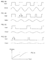
- FIG. 5 shows input and output signals of a switched-mode RF amplifier (e.g., Classes D, E, and F) having improved efficiencies at four different output power levels. Time is shown in the horizontal direction in FIG. 5.
- FIG. 5A shows an input rectangular signal that has a 50% duty cycle, which is to say that the input signal is a square wave, and the corresponding output signal. As explained above, a square-wave input results in maximum power out of the amplifier.
- the amplifier's output power is lowered by reducing the widths of a first set of pulses, instead of the conventional technique of reducing the widths of all pulses simultaneously.
- the first set of pulses is every other pulse of the original input signal (shown in FIG.
- FIG. 5A two such reduced-width pulses are shown in FIG. 5B .
- FIG. 5C the widths of the pulses of the first set have been reduced to the point that the first set of pulses has completely disappeared.
- the amplifier is switching at half of the previous rate, effectively halving switch losses and boosting efficiency.
- the output signal depicted in FIG. 5 is that after filtering, and so the output shown in FIG. 5C (and FIG. 5D ) is a harmonic rather than the fundamental of the input signal frequency.
- output power is further reduced by reducing the widths of the remaining pulses.
- the artisan will note the contrast with techniques like the Doherty amplifier.
- the inventor's technique improves amplifier efficiency locally around a point at less than maximum output by changing the signal itself, avoiding a need for multiple component amplifiers and all of the design issues (e.g., matching gains, delays, etc.) inherent in multi-amplifier configurations.
- FIG. 6 illustrates the effect on amplifier efficiency of reducing the widths of selected sets of pulses, such as those depicted in FIG. 5.
- FIG. 6 is a plot of amplifier efficiency against output power, roughly illustrating how the efficiency behaves for the case when the width of every other input signal pulse is reduced to zero (indicated by the vertical dashed line).
- the probability density of output power for an illustrative input AM signal can be the same as that depicted in FIG. 4B .
- Comparison of FIG. 6 with FIG. 4A reveals that at high power, the efficiency behaves in a similar manner as before, but at lower powers (i.e., to the left-hand side of the vertical dashed line in FIG. 6 ), reducing the widths of a selected set of pulses improves the efficiency. Because the input signal amplitude spends most of its time at relatively low power in many important systems, including telecommunication systems, the local improvement in efficiency can improve overall efficiency significantly.
- it is possible to reduce or remove every third pulse (n 3) or any other set of pulses deemed suitable. It is even possible to reduce or remove more than one consecutive input pulse at once (e.g., two out of three consecutive pulses). Moreover, more than one set of pulses can be selected.
- the pulse rate can be minimized even further in a similar way.
- the amplifier's switching losses should be reduced to a quarter of their maximum. It will be understood that other sets of pulses can be chosen.
- FIG. 7A is a block diagram of a pulse modulator 700A that can generate an input signal, such as those depicted in FIG. 5 , for a switched-mode amplifier, such as that depicted in FIG. 3 , or that can be used as a PWM in a radio transmitter, such as that depicted in FIG. 1 .
- the modulator 700A includes two conventional PWMs 702, 704, a reference pulse generator 706A, a half-period delay device 708, and a combiner (summer) 710A.
- the PWMs 702, 704 can be implemented by conventional comparator integrated circuits as explained in U.S. Patent Application No. 12/127,126 filed on May 27, 2008, by C.
- the generator 706A produces a rectangular-pulse signal such that the repetition frequency of the pulses is one half of the frequency f 0 desired in the output signal of the modulator 700A. In a telecommunication system, the frequency f 0 would typically be the frequency of the carrier signal.
- the delay device 708 adjusts the two PWMs 702, 704 such that they are substantially 180-degrees apart by adjusting the relative phase of the reference pulses input to the PWMs 702, 704 from the generator 706A.
- An input signal is provided to the modulator 700A at point A in FIG. 7A , which is an input to a pulse selection network 712A that selects a set of pulses whose widths are varied in accordance with the input signal.
- the amplitude of the input signal can be considered as having a normalized range of zero to unity.
- An input signal amplitude of zero to either of the PWMs 702, 704 means that the respective PWM is off, generating no output pulses provided to the combiner 710A.
- the pulse selection network 712A selects every other pulse in the modulator output signal for an input signal in the upper half of its range, with the result that the widths of the selected pulses are varied based on the amplitude of the input signal.
- the selection network 712A includes amplitude limiters 714, 716 and a summer 718 and scale constant 720 that operate to limit the ranges of the PWMs 702, 704 to one-half to unity and zero to one-half, respectively, of the input signal range.
- the selection network 712A can be implemented in many ways, for example, as a suitably programmed device, such as a DSP or a gate array, and that the arrangement depicted in FIG. 7A is just one example.
- the operation of the modulator 700A can be understood by considering the modulator output signal produced by the combiner 710A for some different modulator input signals. For an input signal amplitude of zero, both PWMs 702, 704 are off. For input signal amplitudes between zero and one-half, only PWM 704 is on, which is to say that PWM 704 generates a train of pulses having widths that correspond to the input signal amplitude with a duty cycle less than 25%. For input signal amplitudes between one-half and unity, PWM 704 is fully on (i.e., it generates a pulse train having a duty cycle of 25%), and PWM 702 is on. For an input signal amplitude of unity, both PWMs 702, 704 are fully on and the combiner 710A generates a square wave output signal. This condition is depicted by the pulsed signals shown in FIG. 7A .
- FIG. 7B is a block diagram of a pulse modulator 700B that, like the modulator 700A, can generate an input signal for a switched-mode amplifier or a radio transmitter.
- the modulator 700B includes three conventional PWMs 752, 754, 756, a reference pulse generator 706B, a two-thirds-period delay device 758, a one-third-period delay device 760, and a combiner (summer) 710B.
- the PWMs 752, 754, 756 can be implemented by conventional comparator integrated circuits like the PWMs 702, 704, and like the PWMs 702, 704, together comprise a circuit arrangement configured to generate at least two pulse signals based on a reference pulse signal.
- the generator 706B produces a rectangular-pulse signal such that the repetition frequency of the pulses is one third of the frequency f 0 desired in the output signal of the modulator 700B.
- the delay devices 758, 760 adjust the three PWMs 752, 754, 756 such that they are substantially 120-degrees apart by adjusting the relative phases of the reference pulses input to the PWMs 752, 754, 756 from the generator 706B.
- An input signal is provided to the modulator 700B at point A in FIG. 7B , which is an input to a pulse selection network 712B that selects a set of pulses whose widths are varied in accordance with the input signal.
- the amplitude of the input signal can be considered as having a normalized range of zero to unity, and an input signal amplitude of zero to any of the PWMs 752, 754, 756 means that the respective PWM is off.
- An input amplitude of one third to any of the PWMs 752, 754, 756 results in an output pulse train having a 16.7% duty cycle provided to the combiner 710B.
- the selection network 712B includes amplitude limiters 762, 764, 766, summers 768, 770, and scale constants 772, 774 that operate to limit the ranges of the PWMs 752, 754, 756 to two-thirds to unity, one-third to two-thirds, and zero to one-third, respectively, of the input signal range.
- the selection network 712B can be implemented in many ways, for example, as a suitably programmed device, such as a DSP or a gate array.
- FIGs. 7A , 7B are just two examples of a modulator in which m out of n pulses are selected.
- the modulators 700A, 700B can be divided into more branches, with the limiters operating in smaller intervals.
- the number of PWMs can be reduced to one, although other portions of the modulator get more complicated.
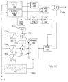
- FIG. 7C is a block diagram of a pulse modulator 700C that is a variation of the modulator 700B having a single PWM 780.
- Components or functional blocks in FIG. 7C that have the same functionality as components or functional blocks in FIG. 7B have the same reference numerals.
- the arrangement depicted in FIG. 7C includes the system of FIG. 7B for selecting among amplitude ranges of the input signal at point A, but that system is supplemented by a selector 782, which responds to a control signal generated by a range selector 784 such that it passes one of the three amplitude ranges to the PWM 780.
- a suitable selector 784 can include two comparators and two voltage references.
- a more complicated selector 784 can include an A/D converter and a logic network, such as a DSP.
- the PWM 780 starts at zero for an input of 0, and reaches its maximum (i.e., 16.7% duty cycle) for an input signal amplitude of 1/3. As the input amplitude becomes greater than 1/3, the PWM 780 begins at zero again, while one of the additional sets of reference pulses is added to the output produced by the combiner 710B by the pulse generator 706B and a network comprising selectable generators 786, 788, logical AND gates 790, 792, and one-third-period delay devices 794, 796. As the input signal amplitude becomes greater than 2/3, the PWM 780 begins at zero once again, while another of the additional sets of reference pulses is added to the output.
- Each generator 786, 788 provides either a logical zero or a logical one signal to the AND gates 790, 792, respectively, depending on the amplitude of the input signal at point A.
- the AND gates 790, 792 pass or block pulses from the generator 706B.
- the fully on or fully off PWMs in the arrangements shown in FIGs. 7A , 7B have been replaced by passing or blocking a set of reference pulses.
- the PWM 780 and the AND gates 790, 792 together comprise a circuit arrangement configured to generate at least two pulse signals based on a reference pulse signal. It will be noted that in the arrangement of FIG. 7C , only one set of reference pulses is width-modulated.
- Each pulse edge introduces some nonlinearity into the combined signal produced by the combiner 710A, 710B.
- Such nonlinearity results in part from the practical inability of the PWMs to produce vertical pulse edges. This may be compensated by suitably predistorting the input signal, which can be carried out in many well known ways. It may also be possible to even out the transitions by introducing some overlap where both PWMs 702, 704 or PWM pairs 752, 754, and 754, 756 are modulated.
- transitions occur at input signal amplitudes around 0.5
- transitions occur at input signal amplitudes around 1/3 and 2/3.
- one pulse width modulator is trying to produce very thin pulses when the input signal amplitude is just above 0.5. Because it is impossible to produce infinitely narrow pulses, there is likely to be some distortion at this point. Of course, overlap is not possible with the arrangement depicted in FIG. 7C that uses only one PWM.
- Nonlinearities can also be compensated by providing low-pass-filtered feedback.
- BP-PWM the envelope of the input signal has a sinusoidal, and thus non-linear, relationship to the duty cycle of the output.
- Modulators of this type can be linearized using low-pass feedback, as described in the document by M. Nielsen et al. and WO 2008/002225 cited above and in U.S. Patent Application No. 12/135,326 filed on June 9, 2008, by Carl Bryant for "Quadrature Pulse-Width Modulation Methods and Apparatus".
- a suitable arrangement look like its FIG. 6 , with the PWM 602 representing the modulator 700A, 700B.
- the modulator 700A, 700B includes two (or more) component PWMs, low-pass-filtered feedback can be used globally to cancel amplitude distortion.
- switch noise may be introduced into the amplifier output signal at frequencies that are m/n and (n-m)/n of the carrier frequency away from the carrier frequency.
- a suitable filter may be needed to eliminate or reduce such switch noise sufficiently. As the number of pulses is reduced, the filter requirements become more stringent.
- Effects of switch noise can be reduced by randomly or pseudorandomly selecting sets of pulses. For example, whether a pulse is to be pulse-width modulated can be randomly or pseudorandomly determined at the time of the pulse, with a time-average of the number of pulse-width modulated pulses being such that the desired amplifier performance is obtained. Randomizing the pulse selection in this way should spread out the switch noise, although the signal to the PWMs would vary with time.
- the selector 800 comprises delay devices 802-1, 802-2, ..., which time delay reference pulses produced by a generator 706 by respective fractions m/n of a period T, where m and n are positive integers and m ⁇ n as described above.
- the period T may be the inverse of the frequency f 0 desired in the output signal of the modulator 700A, 700B, 700C, and the generator 706 is comparable to the generators 706A, 706B, producing pulses at repetition frequency that is a fraction (1/n) of the frequency f 0 .
- the selector also comprises a pulse distributor 804 that is responsive to a control signal produced by a generator 806 and that can be considered a controllable switch. The control signal is such that delayed pulses appear at respective outputs of the distributor 804 in a desired random or pseudorandom fashion.
- the pulse selector 800 does not, strictly speaking, randomize the number of reference pulses in a given time period produced by the pulse generators 706A, 706B, but instead the selector 800 randomizes the phases of the selected pulses.
- the modulators 700A, 700B, 700C all reference pulse inputs would be connected to a randomly selected output in the selector 800, and the number of delay devices 802 would typically be N-1.
- FIG. 8 depicts an extended generalization of a pulse selector for generating N pulse sets, and so to make a complete modulator, the selector 800 of FIG. 8 is combined with PWMs and a suitable pulse selection network 712A, 7128, extended if needed for N > 3 different control intervals.
- the reference phases are different (i.e., 0T, 1T, 2T, ..., (N-1)T)
- the n-th overtones of all pulse sets have substantially the same phase, and so the sets can be randomly interleaved without substantially affecting the desired signal.
- FIG. 9 is a block diagram of one example of a suitable arrangement 900 for adjusting the phases of reference pulses (i.e., the pulses' positions in time).
- a pulsed phase information signal which is often a signal at the frequency f 0 desired in the output signal of the pulse modulator, switched-mode amplifier, or transmitter, is provided to a frequency divider 902, which produces a phase signal having pulses at a frequency that is a fraction (1/n) of the frequency f 0 .
- Delay devices 904-1, 904-2, ... time-delay the pulses produced by the divider 902 by respective fractions m/n of a period T, where m, n, and T are as described above. It will be observed that the difference between the networks 900 and 800 is the distributor 804 and generator 806.
- FIG. 10 is a flowchart of a method of generating selected pulses of controllable widths based on an input signal, such as the method implemented by the modulators 700A, 700B, 700C.
- a pulse signal based on a reference pulse signal is generated, and in step 1004, a set of pulses in the generated pulse signal is selected based on the input signal.
- the widths of the pulses in the selected set are controlled in accordance with the input signal.
- An example of selection of every other pulse is performed by the network 712A described above, and controlling widths can include generating at least two signals that each have an amplitude range that is substantially one-half of an amplitude range of the input signal.
- at least one low-pass-filtered feed-back signal based on the pulse signal can be generated and added to the input signal.
- switched-mode amplifier efficiency should increase for smaller input signals due to lower switching losses.
- High small-signal efficiency is important for maximizing overall efficiency with modern modulations that demand close to maximum output power only a fraction of the time.
- the advantages of the methods and apparatus described in this application can be enjoyed with no need for multiple amplifiers, reducing the cost and complexity of a switched-mode amplifier.
- RF PWM a modulator needs to handle minute changes in time accurately while modulating the envelope, and so it can be expected that the above-described methods and apparatus can improve the modulation accuracy because relative changes in pulse width are increased when only a subset of pulses, such as every other pulse, is modulated.
- this invention can additionally be considered to be embodied entirely within any form of computer-readable storage medium having stored therein an appropriate set of instructions for use by or in connection with an instruction-execution system, apparatus, or device, such as a computer-based system, processor-containing system, or other system that can fetch instructions from a medium and execute the instructions.
- a "computer-readable medium” can be any means that can contain, store, communicate, or transport the program for use by or in connection with the instruction-execution system, apparatus, or device.
- the computer-readable medium can be, for example but not limited to, an electronic, magnetic, optical, electromagnetic, infrared, or semiconductor system, apparatus, device, or medium.
- the computer-readable medium include an electrical connection having one or more wires, a portable computer diskette, a random-access memory (RAM), a read-only memory (ROM), an erasable programmable read-only memory (EPROM or Flash memory), and an optical fiber.
- RAM random-access memory
- ROM read-only memory
- EPROM or Flash memory erasable programmable read-only memory
- any such form may be referred to as "logic configured to” perform a described action, or alternatively as “logic that” performs a described action.
Landscapes
- Engineering & Computer Science (AREA)
- Power Engineering (AREA)
- Physics & Mathematics (AREA)
- Spectroscopy & Molecular Physics (AREA)
- Computer Networks & Wireless Communication (AREA)
- Signal Processing (AREA)
- Amplifiers (AREA)
Claims (15)
- Pulsmodulator zum Erzeugen eines Ausgangspulssignals mit einem ausgewählten Satz von Pulsen mit regelbaren Breiten, umfassend:einen Referenzpulsgenerator (706, 706A, 706B), der zum Erzeugen eines Referenzpulssignals (Φ) ausgelegt ist;eine Schaltkreisanordnung, die zum Erzeugen von mindestens zwei Pulssignalen auf der Basis des Referenzpulssignals (Φ) konfiguriert ist, wobei die Schaltkreisanordnung mindestens einen Pulsbreitenmodulator, PWM, (702, 704; 752, 754, 756; 780) umfasst;mindestens eine Verzögerungsvorrichtung (708; 758, 760; 794, 796; 802-1, 802-2; 904-1, 904-2), die zum zeitweiligen Verschieben der mindestens zwei Pulssignale gegeneinander um einen Bruchteil einer Periode des Ausgangspulssignals, durch Einstellen der relativen Phase von Referenzpulsen des Referenzpulssignals (Φ), die in die Schaltkreisanordnung eingegeben werden, konfiguriert ist;ein Pulsauswahlnetzwerk (712A, 712B), das konfiguriert ist zum Aufnehmen eines Pulsmodulator-Eingangssignals (A); zum Übermitteln des Pulsmodulator-Eingangssignals an verschiedene Teile der Schaltkreisanordnung auf der Basis unterschiedlicher Amplitudenbereiche des Pulsmodulator-Eingangssignals, und zusammen mit dem mindestens einen PWM, zum Steuern des Auswählens eines Satzes von Pulsen aus den mindestens zwei Pulssignalen, wobei die Breiten des ausgewählten Satzes von Pulsen auf der Basis der Amplitude des Pulsmodulator-Eingangssignals (A) variiert werden; undeinen Kombinator (710A, 710B), der zum Kombinieren des ausgewählten Satzes von Pulsen und Erzeugen des Ausgangspulssignals des Pulsmodulators konfiguriert ist.
- Pulsmodulator nach Anspruch 1, wobei die Schaltkreisanordnung mindestens zwei PWMs (702, 704; 752, 754, 756) umfasst; das Pulsauswahlnetzwerk (712A, 712B) zum Erzeugen von mindestens zwei Eingangssignalen jeweils für einen der mindestens zwei PWMs (702, 704; 752, 754, 756) aus dem Pulsmodulator-Eingangssignal (A) konfiguriert ist; jedes der mindestens zwei Eingangssignale einen Amplitudenbereich hat, der im Wesentlichen eine Hälfte eines Amplitudenbereichs des Pulsmodulator-Eingangssignals ist; und die Amplitudenbereiche der mindestens zwei Eingangssignale sich im Wesentlichen nicht überlappen.
- Pulsmodulator nach Anspruch 1, wobei die Schaltkreisanordnung einen PWM (780) und mindestens ein logisches AND-Gatter (790, 792) umfasst und der Pulsmodulator ferner eine Vorrichtung (782) zum Wählen eines Amplitudenbereichs und Zuführen des Pulsmodulator-Eingangssignals (A) im gewählten Amplitudenbereich zum PWM (780) umfasst, wobei das mindestens eine logische AND-Gatter, das zwischen dem Referenzpulsgenerator (706B) und dem Kombinator (710B) liegt, zum Aufnehmen eines Kontrollsignals konfiguriert ist, um, je nach der Amplitude des Pulsmodulator-Eingangssignals, die Referenzpulse vom Referenzpulsgenerator (706B) zum Kombinator (710B) passieren zu lassen oder zu blockieren.
- Pulsmodulator nach Anspruch 1, wobei das Pulsauswahlnetzwerk zusammen mit dem mindestens einen PWM zum Steuern der Auswahl von m aus n Pulsen der mindestens zwei Pulssignale konfiguriert ist, m und n ganze Zahlen sind und m < n ist.
- Pulsmodulator nach Anspruch 1, wobei das Pulsauswahlnetzwerk zum zufälligen oder pseudozufälligen Bestimmen der Auswahl des Satzes von Pulsen konfiguriert ist.
- Pulsmodulator nach Anspruch 1, der ferner ein Phasennetzwerk umfasst, das zum Einstellen von Phasen der Referenzpulse auf der Basis von Phaseninformationen im Pulsmodulator-Eingangssignal konfiguriert ist.
- Pulsmodulator nach Anspruch 1, wobei der Pulsmodulator in einem Schaltverstärker enthalten ist.
- Pulsmodulator nach Anspruch 1, wobei der Pulsmodulator in einem HF-Sender enthalten ist.
- Verfahren zum Erzeugen eines Ausgangspulssignals mit einem ausgewählten Satz von Pulsen von regelbarer Breite auf der Basis eines Eingangssignals, umfassend:Erzeugen eines Referenzpulssignals (Φ);Erzeugen (1002) von mindestens zwei Pulssignalen auf der Basis des Referenzpulssignals (Φ) derart, dass die relativen Phasen der mindestens zwei Pulssignale zeitweilig gegeneinander um einen Bruchteil einer Periode des Ausgangspulssignals verschoben werden, indem relative Phasen von Referenzpulsen der Referenzpulse des Referenzpulssignals (Φ) eingestellt werden;Auswählen (1004) eines Satzes von Pulsen der mindestens zwei Pulssignale durch Übermitteln des Eingangssignals an die erzeugten mindestens zwei Pulssignale auf der Basis von unterschiedlichen Amplitudenbereichen des Eingangssignals, wobei der ausgewählte Satz weniger als alle Pulse in den erzeugten mindestens zwei Pulssignalen enthält;Steuern (1006) der Breiten des ausgewählten Satzes von Pulsen auf der Basis der Amplitude des Eingangssignals derart, dass die Breite variiert wird; undKombinieren des ausgewählten Satzes von Pulsen derart, dass das Ausgangspulssignal erzeugt wird.
- Verfahren nach Anspruch 9, wobei das Steuern von Breiten das Erzeugen von mindestens zwei Signalen, die jeweils einen Amplitudenbereich haben, welcher im Wesentlichen eine Hälfte eines Amplitudenbereichs des Eingangssignals ausmacht, aus dem Eingangssignal umfasst; und die Amplitudenbereiche der mindestens zwei Signale sich im Wesentlichen nicht überlappen.
- Verfahren nach Anspruch 9, das ferner das Auswählen eines Amplitudenbereichs umfasst, wobei die Breiten der Pulse im ausgewählten Satz entsprechend dem Eingangssignal im ausgewählten Amplitudenbereich geregelt werden.
- Verfahren nach Anspruch 9, wobei das Auswählen (1004) eines Satzes von Pulsen das Auswählen von m aus n Pulsen der mindestens zwei Pulssignale umfasst, m und n ganze Zahlen sind und m<n ist.
- Verfahren nach Anspruch 9, wobei das Auswählen (1004) eines Satzes von Pulsen das zufällige oder pseudozufällige Auswählen von Pulsen der mindestens zwei Pulssignale umfasst.
- Verfahren nach Anspruch 9, wobei das Einstellen von relativen Phasen von Referenzpulsen, die im Referenzpulssignal verwendet werden, auf Phaseninformationen im Eingangssignal beruht.
- Computerprogramm, das Anweisungen hat, die bei Ausführung durch den Computer bewirken, dass ein Computer das Verfahren zum Erzeugen eines Ausgangspulssignals mit ausgewählten Pulsen von regelbarer Breite nach einem der Ansprüche 9 bis 14 ausführt.
Applications Claiming Priority (2)
| Application Number | Priority Date | Filing Date | Title |
|---|---|---|---|
| US12/246,031 US7863956B2 (en) | 2008-10-06 | 2008-10-06 | Pulse-elimination pulse-width modulation |
| PCT/EP2009/062832 WO2010040692A1 (en) | 2008-10-06 | 2009-10-02 | Pulse-width modulation with selective pulse-eliminator |
Publications (2)
| Publication Number | Publication Date |
|---|---|
| EP2332251A1 EP2332251A1 (de) | 2011-06-15 |
| EP2332251B1 true EP2332251B1 (de) | 2013-12-11 |
Family
ID=41413085
Family Applications (1)
| Application Number | Title | Priority Date | Filing Date |
|---|---|---|---|
| EP09783694.4A Not-in-force EP2332251B1 (de) | 2008-10-06 | 2009-10-02 | Pulsbreitenmodulation mit selektiver Pulseliminierung |
Country Status (4)
| Country | Link |
|---|---|
| US (1) | US7863956B2 (de) |
| EP (1) | EP2332251B1 (de) |
| CN (1) | CN102239635B (de) |
| WO (1) | WO2010040692A1 (de) |
Families Citing this family (9)
| Publication number | Priority date | Publication date | Assignee | Title |
|---|---|---|---|---|
| CN101796712B (zh) * | 2007-09-25 | 2013-03-27 | 株式会社大亨 | Pwm信号生成装置和具有该pwm信号生成装置的逆变装置 |
| US8195109B2 (en) * | 2010-03-23 | 2012-06-05 | Texas Instruments Incorporated | Single ended switched power amplifier with tuned load coupling block |
| US8878622B2 (en) | 2011-04-07 | 2014-11-04 | Infineon Technologies Ag | System and method for generating a pulse-width modulated signal |
| US8971398B2 (en) | 2011-09-19 | 2015-03-03 | Infineon Technologies Ag | System and method for generating a radio frequency pulse-width modulated signal |
| US9252995B2 (en) * | 2012-08-27 | 2016-02-02 | Telefonaktiebolaget L M Ericsson (Publ) | Transmission of pulse length modulation information |
| TW201419761A (zh) * | 2012-11-12 | 2014-05-16 | Inno Tech Co Ltd | 正弦波脈衝寬度調變控制器 |
| US20140368278A1 (en) * | 2013-06-18 | 2014-12-18 | Auriga Measurement Systems, LLC | Using Multiple-Driver Stages to Realize Fast Rise/Fall Time And Large Current Capability |
| US9660632B1 (en) | 2015-12-16 | 2017-05-23 | Cirrus Logic, Inc. | Adjustable time duration for driving pulse-width modulation (PWM) output to reduce thermal noise |
| CN114172768B (zh) * | 2021-12-06 | 2024-01-26 | 中国人民解放军国防科技大学 | 一种基于移相控制的射频脉宽调制方法、调制器及发信机 |
Family Cites Families (9)
| Publication number | Priority date | Publication date | Assignee | Title |
|---|---|---|---|---|
| US5657215A (en) | 1995-08-29 | 1997-08-12 | Compaq Computer Corporation | Controlling switch-Mode power conversion |
| US6130910A (en) | 1997-11-03 | 2000-10-10 | Motorola, Inc. | Method and apparatus for high efficiency wideband power amplification |
| KR100453708B1 (ko) | 2000-11-03 | 2004-10-20 | 네오피델리티 주식회사 | 고효율 스위칭 증폭기 |
| US6538484B1 (en) * | 2002-03-18 | 2003-03-25 | Lynx-Photonic Networks Ltd. | High-frequency PWM voltage control |
| US7078963B1 (en) | 2003-03-21 | 2006-07-18 | D2Audio Corporation | Integrated PULSHI mode with shutdown |
| US6970051B2 (en) | 2003-12-08 | 2005-11-29 | Harris Corporation | Pulse width modulator circuit having negative bias |
| KR100618408B1 (ko) | 2005-05-17 | 2006-08-31 | (주)펄서스 테크놀러지 | 디지털 앰프용 펄스 폭 변조기, 디지털 앰프의 팝 노이즈감소 방법 및 디지털 앰프 |
| GB2429351B (en) | 2005-08-17 | 2009-07-08 | Wolfson Microelectronics Plc | Feedback controller for PWM amplifier |
| JP4960449B2 (ja) | 2006-06-27 | 2012-06-27 | テレフオンアクチーボラゲット エル エム エリクソン(パブル) | スイッチモード電力増幅 |
-
2008
- 2008-10-06 US US12/246,031 patent/US7863956B2/en not_active Expired - Fee Related
-
2009
- 2009-10-02 EP EP09783694.4A patent/EP2332251B1/de not_active Not-in-force
- 2009-10-02 CN CN200980149065.XA patent/CN102239635B/zh not_active Expired - Fee Related
- 2009-10-02 WO PCT/EP2009/062832 patent/WO2010040692A1/en not_active Ceased
Also Published As
| Publication number | Publication date |
|---|---|
| US20100085097A1 (en) | 2010-04-08 |
| US7863956B2 (en) | 2011-01-04 |
| CN102239635A (zh) | 2011-11-09 |
| CN102239635B (zh) | 2014-10-15 |
| EP2332251A1 (de) | 2011-06-15 |
| WO2010040692A1 (en) | 2010-04-15 |
Similar Documents
| Publication | Publication Date | Title |
|---|---|---|
| EP2332251B1 (de) | Pulsbreitenmodulation mit selektiver Pulseliminierung | |
| Varlamov et al. | Simultaneous application of several synthetic methods for high efficiency radiofrequency amplification | |
| Hung et al. | Design of H-bridge class-D power amplifiers for digital pulse modulation transmitters | |
| US7884667B2 (en) | Pulse area modulation and high-efficiency linear power amplifier system using the same | |
| US8693578B2 (en) | Transmission device | |
| US20090149151A1 (en) | Quadrature Pulse-Width Modulation Methods and Apparatus | |
| US8970295B2 (en) | System and method for a power amplifier | |
| Watkins et al. | How not to rely on Moore's Law alone: low-complexity envelope-tracking amplifiers | |
| CN101557202B (zh) | 大功率d类功率放大器 | |
| Hühn et al. | A new modulator for digital RF power amplifiers utilizing a wavetable approach | |
| Chen et al. | A polar-transmitter architecture using multiphase pulsewidth modulation | |
| CN101473529B (zh) | 开关模式功率放大 | |
| Ibrahimov et al. | Efficiency analysis of switching converter-modulator | |
| WO2007069191A2 (en) | Multi-mode modulation apparatus | |
| GB2456889A (en) | A PWM modulator for a Cartesian transmitter | |
| Blocher et al. | Coding efficiency for different switched-mode RF transmitter architectures | |
| EP2670101B1 (de) | Verfahren zur Pulsweitenmodulation eines Signals | |
| US20090146754A1 (en) | Pulse-Width Modulator Methods and Apparatus | |
| Huhn et al. | GaN-Based digital transmitter chain utilizing push-pull gate drivers for high switching speed and built-in DPD | |
| Sajedin et al. | A Doherty power amplifier based on the harmonic generating mechanism | |
| Arian et al. | Power‐efficient burst‐mode RF transmitter based on reference‐adaptive multilevel pulse‐width modulation | |
| US20120250754A1 (en) | Efficiency-optimized coding for high frequency power amplifiers | |
| Zhao et al. | Enhancing the efficiency of PA with envelope tracking power supply triggering synchronization | |
| Sjöland et al. | Switched mode transmitter architectures | |
| CN218633891U (zh) | 一种函数波形调制电路 |
Legal Events
| Date | Code | Title | Description |
|---|---|---|---|
| PUAI | Public reference made under article 153(3) epc to a published international application that has entered the european phase |
Free format text: ORIGINAL CODE: 0009012 |
|
| 17P | Request for examination filed |
Effective date: 20110406 |
|
| AK | Designated contracting states |
Kind code of ref document: A1 Designated state(s): AT BE BG CH CY CZ DE DK EE ES FI FR GB GR HR HU IE IS IT LI LT LU LV MC MK MT NL NO PL PT RO SE SI SK SM TR |
|
| AX | Request for extension of the european patent |
Extension state: AL BA RS |
|
| DAX | Request for extension of the european patent (deleted) | ||
| 17Q | First examination report despatched |
Effective date: 20120808 |
|
| REG | Reference to a national code |
Ref country code: DE Ref legal event code: R079 Ref document number: 602009020722 Country of ref document: DE Free format text: PREVIOUS MAIN CLASS: H03F0003217000 Ipc: H03F0001020000 |
|
| GRAP | Despatch of communication of intention to grant a patent |
Free format text: ORIGINAL CODE: EPIDOSNIGR1 |
|
| INTG | Intention to grant announced |
Effective date: 20130806 |
|
| RIC1 | Information provided on ipc code assigned before grant |
Ipc: H03F 3/24 20060101ALI20130726BHEP Ipc: H03F 3/19 20060101ALI20130726BHEP Ipc: H03F 3/217 20060101ALI20130726BHEP Ipc: H03K 7/08 20060101ALI20130726BHEP Ipc: H03F 1/02 20060101AFI20130726BHEP Ipc: H04L 25/49 20060101ALI20130726BHEP Ipc: H03K 3/017 20060101ALI20130726BHEP |
|
| GRAS | Grant fee paid |
Free format text: ORIGINAL CODE: EPIDOSNIGR3 |
|
| GRAA | (expected) grant |
Free format text: ORIGINAL CODE: 0009210 |
|
| AK | Designated contracting states |
Kind code of ref document: B1 Designated state(s): AT BE BG CH CY CZ DE DK EE ES FI FR GB GR HR HU IE IS IT LI LT LU LV MC MK MT NL NO PL PT RO SE SI SK SM TR |
|
| REG | Reference to a national code |
Ref country code: GB Ref legal event code: FG4D |
|
| REG | Reference to a national code |
Ref country code: CH Ref legal event code: EP |
|
| REG | Reference to a national code |
Ref country code: AT Ref legal event code: REF Ref document number: 645026 Country of ref document: AT Kind code of ref document: T Effective date: 20140115 |
|
| REG | Reference to a national code |
Ref country code: IE Ref legal event code: FG4D |
|
| REG | Reference to a national code |
Ref country code: DE Ref legal event code: R096 Ref document number: 602009020722 Country of ref document: DE Effective date: 20140206 |
|
| REG | Reference to a national code |
Ref country code: NL Ref legal event code: VDEP Effective date: 20131211 |
|
| REG | Reference to a national code |
Ref country code: AT Ref legal event code: MK05 Ref document number: 645026 Country of ref document: AT Kind code of ref document: T Effective date: 20131211 |
|
| PG25 | Lapsed in a contracting state [announced via postgrant information from national office to epo] |
Ref country code: HR Free format text: LAPSE BECAUSE OF FAILURE TO SUBMIT A TRANSLATION OF THE DESCRIPTION OR TO PAY THE FEE WITHIN THE PRESCRIBED TIME-LIMIT Effective date: 20131211 Ref country code: FI Free format text: LAPSE BECAUSE OF FAILURE TO SUBMIT A TRANSLATION OF THE DESCRIPTION OR TO PAY THE FEE WITHIN THE PRESCRIBED TIME-LIMIT Effective date: 20131211 Ref country code: NO Free format text: LAPSE BECAUSE OF FAILURE TO SUBMIT A TRANSLATION OF THE DESCRIPTION OR TO PAY THE FEE WITHIN THE PRESCRIBED TIME-LIMIT Effective date: 20140311 Ref country code: SE Free format text: LAPSE BECAUSE OF FAILURE TO SUBMIT A TRANSLATION OF THE DESCRIPTION OR TO PAY THE FEE WITHIN THE PRESCRIBED TIME-LIMIT Effective date: 20131211 Ref country code: LT Free format text: LAPSE BECAUSE OF FAILURE TO SUBMIT A TRANSLATION OF THE DESCRIPTION OR TO PAY THE FEE WITHIN THE PRESCRIBED TIME-LIMIT Effective date: 20131211 Ref country code: NL Free format text: LAPSE BECAUSE OF FAILURE TO SUBMIT A TRANSLATION OF THE DESCRIPTION OR TO PAY THE FEE WITHIN THE PRESCRIBED TIME-LIMIT Effective date: 20131211 |
|
| REG | Reference to a national code |
Ref country code: LT Ref legal event code: MG4D |
|
| PG25 | Lapsed in a contracting state [announced via postgrant information from national office to epo] |
Ref country code: LV Free format text: LAPSE BECAUSE OF FAILURE TO SUBMIT A TRANSLATION OF THE DESCRIPTION OR TO PAY THE FEE WITHIN THE PRESCRIBED TIME-LIMIT Effective date: 20131211 Ref country code: CY Free format text: LAPSE BECAUSE OF FAILURE TO SUBMIT A TRANSLATION OF THE DESCRIPTION OR TO PAY THE FEE WITHIN THE PRESCRIBED TIME-LIMIT Effective date: 20131211 Ref country code: AT Free format text: LAPSE BECAUSE OF FAILURE TO SUBMIT A TRANSLATION OF THE DESCRIPTION OR TO PAY THE FEE WITHIN THE PRESCRIBED TIME-LIMIT Effective date: 20131211 |
|
| PG25 | Lapsed in a contracting state [announced via postgrant information from national office to epo] |
Ref country code: EE Free format text: LAPSE BECAUSE OF FAILURE TO SUBMIT A TRANSLATION OF THE DESCRIPTION OR TO PAY THE FEE WITHIN THE PRESCRIBED TIME-LIMIT Effective date: 20131211 Ref country code: IS Free format text: LAPSE BECAUSE OF FAILURE TO SUBMIT A TRANSLATION OF THE DESCRIPTION OR TO PAY THE FEE WITHIN THE PRESCRIBED TIME-LIMIT Effective date: 20140411 Ref country code: BE Free format text: LAPSE BECAUSE OF FAILURE TO SUBMIT A TRANSLATION OF THE DESCRIPTION OR TO PAY THE FEE WITHIN THE PRESCRIBED TIME-LIMIT Effective date: 20131211 |
|
| PG25 | Lapsed in a contracting state [announced via postgrant information from national office to epo] |
Ref country code: RO Free format text: LAPSE BECAUSE OF FAILURE TO SUBMIT A TRANSLATION OF THE DESCRIPTION OR TO PAY THE FEE WITHIN THE PRESCRIBED TIME-LIMIT Effective date: 20131211 Ref country code: PT Free format text: LAPSE BECAUSE OF FAILURE TO SUBMIT A TRANSLATION OF THE DESCRIPTION OR TO PAY THE FEE WITHIN THE PRESCRIBED TIME-LIMIT Effective date: 20140411 Ref country code: ES Free format text: LAPSE BECAUSE OF FAILURE TO SUBMIT A TRANSLATION OF THE DESCRIPTION OR TO PAY THE FEE WITHIN THE PRESCRIBED TIME-LIMIT Effective date: 20131211 Ref country code: SK Free format text: LAPSE BECAUSE OF FAILURE TO SUBMIT A TRANSLATION OF THE DESCRIPTION OR TO PAY THE FEE WITHIN THE PRESCRIBED TIME-LIMIT Effective date: 20131211 Ref country code: PL Free format text: LAPSE BECAUSE OF FAILURE TO SUBMIT A TRANSLATION OF THE DESCRIPTION OR TO PAY THE FEE WITHIN THE PRESCRIBED TIME-LIMIT Effective date: 20131211 Ref country code: CZ Free format text: LAPSE BECAUSE OF FAILURE TO SUBMIT A TRANSLATION OF THE DESCRIPTION OR TO PAY THE FEE WITHIN THE PRESCRIBED TIME-LIMIT Effective date: 20131211 |
|
| REG | Reference to a national code |
Ref country code: DE Ref legal event code: R097 Ref document number: 602009020722 Country of ref document: DE |
|
| PLBE | No opposition filed within time limit |
Free format text: ORIGINAL CODE: 0009261 |
|
| STAA | Information on the status of an ep patent application or granted ep patent |
Free format text: STATUS: NO OPPOSITION FILED WITHIN TIME LIMIT |
|
| PG25 | Lapsed in a contracting state [announced via postgrant information from national office to epo] |
Ref country code: DK Free format text: LAPSE BECAUSE OF FAILURE TO SUBMIT A TRANSLATION OF THE DESCRIPTION OR TO PAY THE FEE WITHIN THE PRESCRIBED TIME-LIMIT Effective date: 20131211 |
|
| 26N | No opposition filed |
Effective date: 20140912 |
|
| REG | Reference to a national code |
Ref country code: DE Ref legal event code: R097 Ref document number: 602009020722 Country of ref document: DE Effective date: 20140912 |
|
| PG25 | Lapsed in a contracting state [announced via postgrant information from national office to epo] |
Ref country code: SI Free format text: LAPSE BECAUSE OF FAILURE TO SUBMIT A TRANSLATION OF THE DESCRIPTION OR TO PAY THE FEE WITHIN THE PRESCRIBED TIME-LIMIT Effective date: 20131211 |
|
| PG25 | Lapsed in a contracting state [announced via postgrant information from national office to epo] |
Ref country code: MC Free format text: LAPSE BECAUSE OF FAILURE TO SUBMIT A TRANSLATION OF THE DESCRIPTION OR TO PAY THE FEE WITHIN THE PRESCRIBED TIME-LIMIT Effective date: 20131211 Ref country code: LU Free format text: LAPSE BECAUSE OF FAILURE TO SUBMIT A TRANSLATION OF THE DESCRIPTION OR TO PAY THE FEE WITHIN THE PRESCRIBED TIME-LIMIT Effective date: 20141002 |
|
| REG | Reference to a national code |
Ref country code: CH Ref legal event code: PL |
|
| REG | Reference to a national code |
Ref country code: IE Ref legal event code: MM4A |
|
| PG25 | Lapsed in a contracting state [announced via postgrant information from national office to epo] |
Ref country code: CH Free format text: LAPSE BECAUSE OF NON-PAYMENT OF DUE FEES Effective date: 20141031 Ref country code: LI Free format text: LAPSE BECAUSE OF NON-PAYMENT OF DUE FEES Effective date: 20141031 |
|
| REG | Reference to a national code |
Ref country code: FR Ref legal event code: ST Effective date: 20150630 |
|
| PG25 | Lapsed in a contracting state [announced via postgrant information from national office to epo] |
Ref country code: FR Free format text: LAPSE BECAUSE OF NON-PAYMENT OF DUE FEES Effective date: 20141031 |
|
| PG25 | Lapsed in a contracting state [announced via postgrant information from national office to epo] |
Ref country code: IE Free format text: LAPSE BECAUSE OF NON-PAYMENT OF DUE FEES Effective date: 20141002 |
|
| PG25 | Lapsed in a contracting state [announced via postgrant information from national office to epo] |
Ref country code: SM Free format text: LAPSE BECAUSE OF FAILURE TO SUBMIT A TRANSLATION OF THE DESCRIPTION OR TO PAY THE FEE WITHIN THE PRESCRIBED TIME-LIMIT Effective date: 20131211 |
|
| PG25 | Lapsed in a contracting state [announced via postgrant information from national office to epo] |
Ref country code: BG Free format text: LAPSE BECAUSE OF FAILURE TO SUBMIT A TRANSLATION OF THE DESCRIPTION OR TO PAY THE FEE WITHIN THE PRESCRIBED TIME-LIMIT Effective date: 20131211 Ref country code: GR Free format text: LAPSE BECAUSE OF FAILURE TO SUBMIT A TRANSLATION OF THE DESCRIPTION OR TO PAY THE FEE WITHIN THE PRESCRIBED TIME-LIMIT Effective date: 20140312 |
|
| PG25 | Lapsed in a contracting state [announced via postgrant information from national office to epo] |
Ref country code: HU Free format text: LAPSE BECAUSE OF FAILURE TO SUBMIT A TRANSLATION OF THE DESCRIPTION OR TO PAY THE FEE WITHIN THE PRESCRIBED TIME-LIMIT; INVALID AB INITIO Effective date: 20091002 Ref country code: TR Free format text: LAPSE BECAUSE OF FAILURE TO SUBMIT A TRANSLATION OF THE DESCRIPTION OR TO PAY THE FEE WITHIN THE PRESCRIBED TIME-LIMIT Effective date: 20131211 Ref country code: MT Free format text: LAPSE BECAUSE OF FAILURE TO SUBMIT A TRANSLATION OF THE DESCRIPTION OR TO PAY THE FEE WITHIN THE PRESCRIBED TIME-LIMIT Effective date: 20131211 |
|
| PG25 | Lapsed in a contracting state [announced via postgrant information from national office to epo] |
Ref country code: MK Free format text: LAPSE BECAUSE OF FAILURE TO SUBMIT A TRANSLATION OF THE DESCRIPTION OR TO PAY THE FEE WITHIN THE PRESCRIBED TIME-LIMIT Effective date: 20131211 |
|
| PGFP | Annual fee paid to national office [announced via postgrant information from national office to epo] |
Ref country code: IT Payment date: 20191023 Year of fee payment: 11 |
|
| PGFP | Annual fee paid to national office [announced via postgrant information from national office to epo] |
Ref country code: DE Payment date: 20201028 Year of fee payment: 12 Ref country code: GB Payment date: 20201027 Year of fee payment: 12 |
|
| PG25 | Lapsed in a contracting state [announced via postgrant information from national office to epo] |
Ref country code: IT Free format text: LAPSE BECAUSE OF NON-PAYMENT OF DUE FEES Effective date: 20201002 |
|
| REG | Reference to a national code |
Ref country code: DE Ref legal event code: R119 Ref document number: 602009020722 Country of ref document: DE |
|
| GBPC | Gb: european patent ceased through non-payment of renewal fee |
Effective date: 20211002 |
|
| PG25 | Lapsed in a contracting state [announced via postgrant information from national office to epo] |
Ref country code: GB Free format text: LAPSE BECAUSE OF NON-PAYMENT OF DUE FEES Effective date: 20211002 Ref country code: DE Free format text: LAPSE BECAUSE OF NON-PAYMENT OF DUE FEES Effective date: 20220503 |