EP2333644A2 - Energieeffiziente Anzeigevorrichtung mit Objektabtastfähigkeit - Google Patents
Energieeffiziente Anzeigevorrichtung mit Objektabtastfähigkeit Download PDFInfo
- Publication number
- EP2333644A2 EP2333644A2 EP10013950A EP10013950A EP2333644A2 EP 2333644 A2 EP2333644 A2 EP 2333644A2 EP 10013950 A EP10013950 A EP 10013950A EP 10013950 A EP10013950 A EP 10013950A EP 2333644 A2 EP2333644 A2 EP 2333644A2
- Authority
- EP
- European Patent Office
- Prior art keywords
- groups
- signals
- radiation sources
- radiation
- group
- Prior art date
- Legal status (The legal status is an assumption and is not a legal conclusion. Google has not performed a legal analysis and makes no representation as to the accuracy of the status listed.)
- Granted
Links
Images




Classifications
-
- G—PHYSICS
- G06—COMPUTING OR CALCULATING; COUNTING
- G06F—ELECTRIC DIGITAL DATA PROCESSING
- G06F3/00—Input arrangements for transferring data to be processed into a form capable of being handled by the computer; Output arrangements for transferring data from processing unit to output unit, e.g. interface arrangements
- G06F3/01—Input arrangements or combined input and output arrangements for interaction between user and computer
- G06F3/03—Arrangements for converting the position or the displacement of a member into a coded form
- G06F3/041—Digitisers, e.g. for touch screens or touch pads, characterised by the transducing means
- G06F3/042—Digitisers, e.g. for touch screens or touch pads, characterised by the transducing means by opto-electronic means
-
- G—PHYSICS
- G06—COMPUTING OR CALCULATING; COUNTING
- G06F—ELECTRIC DIGITAL DATA PROCESSING
- G06F1/00—Details not covered by groups G06F3/00 - G06F13/00 and G06F21/00
- G06F1/26—Power supply means, e.g. regulation thereof
- G06F1/32—Means for saving power
- G06F1/3203—Power management, i.e. event-based initiation of a power-saving mode
- G06F1/3234—Power saving characterised by the action undertaken
- G06F1/325—Power saving in peripheral device
- G06F1/3262—Power saving in digitizer or tablet
-
- G—PHYSICS
- G06—COMPUTING OR CALCULATING; COUNTING
- G06F—ELECTRIC DIGITAL DATA PROCESSING
- G06F3/00—Input arrangements for transferring data to be processed into a form capable of being handled by the computer; Output arrangements for transferring data from processing unit to output unit, e.g. interface arrangements
- G06F3/01—Input arrangements or combined input and output arrangements for interaction between user and computer
- G06F3/03—Arrangements for converting the position or the displacement of a member into a coded form
- G06F3/041—Digitisers, e.g. for touch screens or touch pads, characterised by the transducing means
- G06F3/0416—Control or interface arrangements specially adapted for digitisers
- G06F3/04166—Details of scanning methods, e.g. sampling time, grouping of sub areas or time sharing with display driving
Definitions
- the present invention refers generally to a display device and more particularly to an object-sensing (e.g., touch-sensing) display device.
- object-sensing e.g., touch-sensing
- An object-sensing device is a device capable of sensing the presence of an object, and sometimes determines the location of the object on the device. Incorporation of object-sensing capability into display devices is becoming increasingly desirable, as it allows the display device itself to also be used as a user input device, eliminating the need for cumbersome components such as keyboards, keypads, and mouse.
- a user can, for example, touch images of buttons on the display to make a selection or type a word.
- Object-sensing display devices can be useful for applications such as automatic telling machines (ATMs), mobile/cellular phones, and personal digital assistants (PDAs).
- ATMs automatic telling machines
- PDAs personal digital assistants
- object-sensing capability requires extra components, adding the object-sensing capability usually results in higher power consumption for the display device. Both from a practical standpoint and an environmental standpoint, object-sensing display apparatuses that can operate at reduced power consumption are desirable.
- the invention is a method for driving a display device that is capable of sensing object presence (e.g., a touch).
- the method entails providing first signals to a sensing circuit that detects a presence of an object by sensing radiation, wherein the sensing circuit includes scan lines for receiving the first signals.
- Second signals are provided to a radiation source array that provides radiation to the sensing circuit, wherein the second signals selectively activate radiation sources in the radiation source array.
- the timings of the first and second signals are synchronized so that radiation is provided to a portion of the sensing circuit receiving the first signals.
- the invention is a method for driving a display device that is capable of object detection.
- An array of infrared radiation sources are divided into a plurality of groups.
- the plurality of groups is activated sequentially one at a time.
- the invention is a display device that includes a sensor array and a radiation source array coupled to each other.
- the sensor array includes sensing circuits, wherein each of the sensing circuits includes a scan line and a sensing transistor that outputs a detection signal when an object is detected and the scan line is receiving a first signal, and wherein the sensing circuits are sequentially activated by a series of first signals.
- the radiation source array emits radiation that is used by the sensing transistor to detect the object, and the radiation sources in the radiation source array are activated by second signals that are synchronized with the first signals.
- the invention is a display device that includes a sensor array and a radiation source array coupled to each other.
- the sensor array includes sensing circuits, wherein each of the sensing circuits includes a scan line and a sensing transistor that outputs a detection signal when an object is detected and the scan line is receiving a first signal, and wherein the sensing circuits are sequentially activated by a series of first signals.
- the radiation source array emits radiation that is used by the sensing transistor to detect the object, and the radiation sources in the radiation source array are activated by second signals that are synchronized with the first signals.
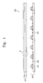
- FIG. 1 is a sectional view showing an exemplary embodiment of a display apparatus having a light source and a radiation source.
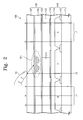
- FIG. 2 is an enlarged view of a portion B of FIG. 1 .
- FIG. 3 is a block diagram of the display apparatus of FIG. 1 .
- FIG. 4 is a plan view of one embodiment of the backlight unit.
- FIG. 5 is a plan view of another embodiment of the backlight unit.
- FIG. 6 is a timing diagram showing the synchronization between the scan signals to a sensing circuit and activation of radiation sources.
- FIG. 7 is a timing diagram showing the turn-on duration of radiation sources when a driving current is increased.
- FIG. 8 is a plan view showing a backlight unit according to another exemplary embodiment of the present invention.
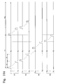
- FIG. 9A is a timing diagram showing the synchronization between the scan signals to a sensing circuit and activation of sub-groups of radiation sources.
- FIG. 9B is a timing diagram showing sub-PWM signals applied to the sub-groups of FIG. 8 .
- FIG. 10A is a timing diagram showing the synchronization between the scan signals to a sensing circuit and activation of sub-groups of radiation sources according to another embodiment of the invention.
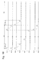
- FIG. 10B is a timing diagram showing sun-PWM signals applied to the sub-groups according to another embodiment of the present invention.
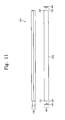
- FIG. 11 is a sectional view of a display apparatus according to another embodiment of the present invention.
- FIG. 12 is a plan view showing the backlight unit of FIG. 11 .
- one way for a display device to detect the presence of an object is by using sensing circuits that have scan lines laid across the display panel.
- the scan line(s) that is closest to that point will indicate the presence and location of the object by generating a signal.
- the signal on the scan line(s) may be generated, for example, by receiving radiation that is reflected by the object.
- radiation sources are often incorporated into the display device to provide the radiation that can be reflected by the object and sensed by the sensing circuit. Typically, the radiation sources are turned on continuously to make sure the object will be detected whenever it is present.
- the invention reduces power consumption dramatically while allowing the object detection to be performed at high accuracy by taking advantage of the fact that the scan lines that detect the radiation reflected by an object may not all be turned on continuously. For example, the scan lines are frequently "scanned" sequentially from one end of the panel to the other.
- the scanning frequency is high relative to the typical duration that an object is present (e.g., duration of a human touch) so that even though not all the scan lines are turned on continuously, there is no concern for a touch or an object presence being missed.
- the invention reduces power consumption by dividing the radiation sources into multiple groups and selectively turning on certain groups of radiation sources as needed, instead of keeping all the radiation sources turned on continuously.
- the radiation sources near the scan lines that are activated may be turned on because an object is sensed by an activated scan line, while others remain turned off. This way, any "wasting" of power from turning on the radiation sources that are not near activated scan lines may be eliminated.
- the structure of the display device with this power-efficient object-sensing capability and the method of detection will now be described.
- a “radiation source” emits radiation that is used for object detection, wherein the radiation may be visible (e.g., white light), invisible (e.g., infrared), or a combination of the two.
- FIG. 1 is a sectional view of a display apparatus according to one embodiment of the present invention.
- a display apparatus 300 includes a display panel 100 and a backlight unit 200 illuminating the display panel 100.
- the display panel 100 includes a lower substrate 110, an upper substrate 120 facing the lower substrate 110, and a liquid crystal layer 125 interposed between the upper and lower substrates 120 and 110.
- the backlight unit 200 includes a circuit substrate 201 provided below the display panel 100, a plurality of light sources 210 (see FIG. 1 ) mounted on the circuit substrate 201 to output a white light L1, and a plurality of radiation sources 220 (see FIG. 1 ) mounted on the circuit substrate 201 to output an infrared ray L2.
- the light source 210 and radiation source 220 are arranged in an alternating manner ⁇ at least one radiation source 220 may be provided between adjacent light sources 210.
- the light sources 210 and radiation sources 220 may include a light emitting diode. As will be explained in more detail below, the light sources 210 are useful for image display and the radiation sources 220 are useful for object detection.
- FIG. 2 is an enlarged view of a portion B of FIG. 1 .
- the lower substrate 110 includes a first base substrate 111 and a plurality of pixels arranged on the first base substrate 111.
- Each pixel includes one of red, green, and blue color pixels R, G, and B, and a pixel electrode 115 provided on the one color pixel.
- Each pixel may further include a thin film transistor in addition to the color pixels R,G, and B and the pixel electrode 115. The structure of each pixel will be described in detail with reference to FIG. 3 .
- a black matrix 112 is arranged between the red, green, and blue color pixels R, G, and B.
- the red, green, and blue color pixels R, G, and B are covered by an organic insulating layer 114.
- the pixel electrode 115 is provided on the organic insulating layer 114.
- the upper substrate 120 includes a second base substrate 121 facing the first base substrate 111 and a plurality of sensors SN (see FIG. 3 ) provided on a bottom surface of the second base substrate 121 facing the lower substrate 110.
- Each sensor SN includes a sensing device (hereinafter, refer to as a sensing transistor ST1).
- the sensing transistor ST1 may include an amorphous silicon transistor.
- the upper substrate 120 further includes an insulating layer 122 that covers the sensors SN and a common electrode 123 provided on the insulating layer 122 to face the pixel electrode 115.
- a liquid crystal capacitor C1c is formed by the pixel electrode 115, the common electrode 123, and the liquid crystal layer 125.
- FIG. 2 shows that the red, green, and blue color pixels R,G, and B are provided in the lower substrate 110, the color pixels R,G, and B may be provided in the upper substrate 120 in some embodiments.
- the white light L1 output from the light sources 210 is supplied to the display panel 100, and the supplied white light L 1 passes through the liquid crystal layer 125.
- Light transmittance of the liquid crystal layer 125 is controlled by an electric field formed between the pixel electrode 115 and the common electrode 123.
- the display panel 100 controls the transmittance of the white light L1 by the liquid crystal layer 125, thereby displaying an image having desired gray scales.
- the infrared ray L2 emitted from the radiation sources 220 is supplied to the display panel 100, and the supplied infrared ray L2 passes through the display panel 100. Since the infrared ray L2 is not visible to a user, the infrared ray L2 does not affect the image displayed on the display panel 100 as perceived by the user. A portion of the infrared ray L2 emitted from the radiation sources 220 is reflected by the layers in the display panel 100. The portion of the infrared ray L2 that is not reflected may pass through the display panel 100 and get radiated outside of the display panel 100. If an object 10 (for example, a finger of a user) is on the display panel 100, the infrared ray L2 reflects off the object 10.
- an object 10 for example, a finger of a user
- the infrared ray L2 that has been reflected by the object 10 may be sensed through the sensing transistor ST1.
- the sensing transistor ST1 outputs a signal that indicates an amount of the reflected infrared ray L2.
- the sensing transistor ST1 may include an amorphous silicon layer.
- the display apparatus 300 determines the location of an object on its surface by using the signal generated from the touch.
- the sensing transistor ST1 When the sensing transistor ST1 is provided on the upper substrate 120, the distance between the object 10 and the sensing transistor ST1 is shorter than it would be if the sensing transistor ST1 were provided on the lower substrate 110. Accordingly, the sensitivity of the sensing transistor ST1 may be improved, and the touch point may be accurately detected. It may be desirable to form the sensing transistor ST1 to overlap the black matrix 112, thereby avoiding decreasing the aperture ratio of the display panel 100.
- the sensors including the sensing transistor ST1 are embedded in the display panel 100 in the embodiment of FIG. 2
- a touch panel (not shown) including the sensors may be provided at an upper portion of the display panel 100 in other embodiments.
- the sensing transistor ST1 may be provided on the lower substrate 110 in some embodiments.
- FIG. 3 is a block diagram showing the display apparatus of FIG. 1 .
- the display apparatus 300 includes a timing controller 130, a data driver 150, a gate driver 140, a read-out circuit 170, a sensor driver 160, and the display panel 100.
- the timing controller 130 receives a plurality of image signals RGB and a plurality of control signals CS from a device outside the display apparatus 300.
- the timing controller 130 converts the data format of the image signals RGB to make them suitable for interface requirements with the data driver 150, and provides the converted image signals R'G'B' to the data driver 150.
- the timing controller 130 provides data control signals (e.g., an output starting signal TP, a horizontal starting signal STH, etc.) to the data driver 150.
- the timing controller 130 provides gate control signals (e.g., a vertical starting signal STV1, a vertical clock signal CK1, and a vertical clock bar signal CKB1) to the gate driver 140.
- the gate driver 140 sequentially outputs gate signals G1 to Gn in response to the gate control signals (the vertical starting signal STV1, the vertical clock signal CK1, and the vertical clock bar signal CKB1) from the timing controller 130.
- the data driver 150 converts the image signals R'G'B' into data voltages D1 to Dm in response to the data control signals (the output starting signal TP and the horizontal starting signal STH) from the timing controller 130 and outputs the data voltages D1 to Dm.
- the data voltages D1 to Dm are applied to the display panel 100.
- the display panel 100 includes a plurality of pixels PX and a plurality of sensors SN.
- the pixels PX and the sensors SN are embedded in the display panel 100.
- the pixels PX are provided in the lower substrate 110, and the sensors SN are provided in the upper substrate 120.
- the lower substrate 110 (shown in FIG. 2 ) includes a plurality of gate lines GL and a plurality of data lines DL crossing the gate lines GL to form the pixels PX.
- Each pixel PX includes a thin film transistor PT, the liquid crystal capacitor Clc, and a storage capacitor Cst.
- the thin film transistor PT includes a gate electrode connected with a gate line corresponding thereto from among the gate lines GL, a source electrode connected with a data line corresponding thereto from among the data lines DL, and a drain electrode connected with the liquid crystal capacitor C1c and the storage capacitor Cst.
- the gate lines GL are connected with the gate driver 140, and the data lines DL are connected with the data driver 150.
- the gate lines GL receive the gate signals G 1 to Gn from the gate driver 140, and the data lines DL receive the data voltages D 1 to Dm from the data driver 150.
- the thin film transistor PT is turned on in response to a gate signal supplied to the corresponding gate line, and the liquid crystal capacitor Clc is charged with a data voltage that has been supplied to the corresponding data line through the thin film transistor PT. Accordingly, each pixel PX may display an image corresponding to the data voltage.
- the upper substrate 120 includes a plurality of scan lines SL, a plurality of read-out lines RL crossing the scan lines SL, and the sensors SN.
- Each sensor SN includes the sensing transistor ST1, a switching transistor ST2, and a capacitor Cs.
- the switching transistor ST2 includes a first electrode connected with a scan line corresponding thereto from among the scan lines SL, a second electrode connected with a read-out line corresponding thereto from among the read-out lines RL, and a third electrode connected with the capacitor Cs and the sensing transistor ST1
- the capacitor Cs has a first electrode connected with the third terminal of the switching transistor ST2 and a second electrode receiving a ground voltage.
- the sensing transistor ST1 includes a first terminal connected with the third terminal of the switching transistor ST2, a second terminal receiving a bias voltage, and a third terminal that is also connected with the second electrode of the capacitor Cs and ground.
- the sensing transistor ST1 senses the infrared ray L2 reflected from the object 10 and outputs a signal corresponding to the amount of the reflected infrared ray L2.
- the amount of charge on the capacitor Cs changes according to the signal output from the sensing transistor ST1. In other words, as the amount of the reflected infrared ray L2 increases, the amount of charge on the capacitor Cs also increases.
- the scan lines SL are connected with the sensor driver 160 to sequentially receive a plurality of scan signals S 1 to Sn, respectively.
- the sensor driver 160 receives sensor control signals STV2, CK2, and CKB2 from the timing controller 130 to output the scan signals S 1 to Sn.
- the sensor control signals STV2, CK2, and CKB2 may be synchronized with the gate control signals (the vertical starting signal STV 1, the vertical clock signal CK1, and the vertical clock bar signal CKB1).
- Each read-out line RL is connected with the read-out circuit 170 to supply the charged voltage of the sensor SN corresponding to each read-out line RL to the read-out circuit 170.
- the sensor SN supplies a charged voltage from the capacitor Cs to the read-out line RL corresponding to the sensor SN.
- the sensing transistor closes, allowing the charge to come out of the capacitor Cs. This drop in the charge on the capacitor Cs is detected when the switching transistor ST2 is turned on, indicating the presence of an object 10.
- the read-out circuit 170 supplies a voltage received from the sensor SN to the timing controller 130.
- the timing controller 130 may create two-dimensional coordinates of a point touched by the object 10 based on a time at which the scan signal is generated and the read-out voltage.
- FIG. 4 is a plan view of a backlight unit.
- the backlight unit 200 includes the circuit substrate 201, the light sources 210 mounted on the circuit substrate 201 to output white light L 1 (shown in FIG. 2 ), and the radiation sources 220 mounted on the circuit substrate 201 to output the infrared ray L2 (shown in FIG. 2 ).
- the light sources 210 are arranged in a matrix, and the radiation sources 220 are arranged in a matrix at positions different from those of the light sources 210.
- the arrangement of the radiation sources 220 are not limited thereto, but may vary according to a total number of the radiation sources 220.
- the number of the radiation sources 220 provided in the backlight unit 200 is approximately equal to the number of the light sources 210.
- a first interval P1 between two first light sources 210 adjacent to each other in a row direction D2 is set to about 27 mm
- a second interval P2 between two first light sources 210 adjacent to each other in a first direction D 1 is set to about 27 mm
- a third interval P3 between two radiation sources 220 adjacent to each other in the row direction D2 is set to about 27 mm
- a fourth interval P4 between two radiation sources 220 adjacent to each other in the first direction D 1 is set to about 27 mm. If the number of the radiation sources 220 is reduced, the third and fourth intervals P3 and P4 may increase.
- FIG. 5 is a plan view showing a backlight unit according to another exemplary embodiment of the invention.
- a backlight unit 205 includes about twice as many radiation sources 220 as light sources 210 in this embodiment.
- the first interval P1 between two light sources 210 adjacent to each other in the row direction D2 is set to about 27 mm
- the second interval P2 between two first light sources 210 adjacent to each other in the first direction D1 is set to about 27 mm
- a fifth interval P5 between two radiation sources 220 adjacent to each other in the row direction D2 is set to about 20 mm
- a sixth interval P6 between two radiation sources 220 adjacent to each other in the first direction D 1 is set to about 19 mm.
- the radiation sources 220 are not used for image display, they are disposed primarily on the inner region of the circuit substrate 201 unlike the light sources 210, which are distributed evenly across the backlight unit 200.
- a distance d1 between a first edge SS1 of the circuit substrate 201 and the light sources 210 closest to the first edge SS1 is set to a value of about 10 mm to about 13 mm, and a distance d2 between the first edge SS1 and the radiation sources 220 closest to the first edge SS1 is set to about 30 mm.
- the first edge SS1 may be a short side of a rectangular substrate.
- distances between a second edge SS2 parallel to the first edge SS 1 and the light sources 210 and radiation sources 220 are set similarly to the distances d1 and d2 between the first edge SS1 and the light sources 210 and radiation sources 220, respectively.
- a distance d3 between a third edge LS1 of the circuit substrate 210 and the light sources 210 closest to the third edge LS1 is set to about 13 mm
- a distance d4 between the third edge LS 1 and the radiation sources 220 closest to the third edge LS1 is set to about 27 mm.
- the third edge LS1 may be a long side of a rectangular substrate.
- distances between a fourth edge LS2 parallel to the third edge LS1 and the light and radiation sources 210 and 220 are set similarly to the distances d3 and d4 between the third edge LS1 and the light and radiation sources 210 and 220.
- the backlight unit 200 and 205 is classified into p groups (hereinafter, referred to as a first group G1 to a sixth group G6) arranged in the first direction D1.
- the first direction D1 is also the direction in which the scan lines SL of the sensors are arranged (see FIG. 3 ).
- "p" is a natural number greater than or equal to 2
- each of the first to sixth groups G1 to G6 includes the radiation sources 220.
- the first to sixth groups G1 to G6 may include the same number of the radiation sources 220.
- each of the first to sixth groups G1 to G6 may include 192 radiation sources 220.
- the first to sixth groups G1 to G6 are shown in FIG. 4 , the invention is not limited to any specific number of groups.
- the first to sixth groups G1 to G6 may be turned on for different durations from each other.
- the turn-on durations of the first to sixth groups G1 to G6 will be described in detail with reference to FIGS. 5 to 6 .
- FIG. 6 is a timing diagram showing turn-on time of the first to sixth groups shown in FIG. 4 and how the scan signals to the sensor are synchronized with pulse width modulation (PWM) signals to radiation sources 220.
- PWM pulse width modulation
- the first to sixth groups receives a first PWM signal PS1 to a sixth PWM signal PS6, respectively.
- the first to sixth PWM signals PS1 to PS6 are sequentially generated during one frame period FR1.
- a high duration of each of the first to sixth PWM signals PS1 to PS6 is defined as a first time period A1.
- the display panel 100 may include k scan lines SL (see FIG. 3 ) corresponding to each of the first to sixth groups G1 to G6.
- the frame period FR1 is set to about 16.3 ms. In this case, the first time period A 1 may be set to about 2.7 ms.
- Each of the 6k scan signals S 1 to S k , S k+1 to S 2k , ..., and S 5k+l to S 6k is generated at a high state for one horizontal scanning period (1Hperiod).
- the high duration of each of the scan signals S 1 to S k may be defined as turn-on duration of each scan line SL.
- the k scan signals S 1 to S k , S k+1 to S 2k , ..., or S 5k+1 to S 6k are sequentially applied to the k scan lines corresponding to each of the first to sixth groups G1 to G6 during the first time period A1.
- k scan signals S 1 to S k are sequentially applied to k scan lines corresponding to the first group G1 during the first time period A1.
- Each of the first to sixth groups G1 to G6 may be turned on for the first time period A1 in which the scan signals S 1 to S k , S k+1 to S 2k , ..., or S 5k+1 to S 6k are applied to the scan lines corresponding to each of the first to sixth groups G1 to G6.
- the radiation sources 220 included in the first group G1 may be consecutively turned on from a rising edge of a first scan signal S1, which is applied to a first scan line from among the k scan lines in the first group G1, to the falling edge of a last scan signal S k which is applied to a last scan line among the k scan lines in the first group G1.
- the first group G1 When the first time period A1 elapses after the first group G1 is turned on, the first group G1 is turned off and the second group G2 is turned on during the next first time period A1. This procedure is repeated so that the first to sixth groups G1 to G6 may be turned on at different times. As shown in FIG. 6 , the first to sixth groups G1 to G6 may be sequentially turned on in the first direction D1. In this case, the turn-on durations of the first to sixth groups G 1 to G6 do not overlap with each other.
- power consumption in the backlight unit 200 may be reduced to about 1/6 as compared with power consumption when the first to sixth groups G1 to G6 are turned on throughout the one frame period FR1.
- the length of the turn-on duration of each of the first to sixth groups G1 to G6 may be adjusted according to the characteristics of the sensing transistor ST1 (shown in FIG. 3 ) provided in the each sensor SN. Since the time (charge time) required to charge the sense signal of the sensing transistor ST2 and the capacitor Cs (shown in FIG. 3 ) corresponds to several micro-seconds, even if the turn-on duration of each of the first to sixth groups G1 to G6 is reduced to about 2.7 ms, the sensors SN may normally sense the infrared ray L2.
- FIG. 7 is a timing diagram showing the turn-on duration of the first to sixth groups when a driving current supplied to the radiation sources of FIG. 4 is increased.
- the driving current supplied to the radiation sources 220 when the high duration of each of the first to sixth PWM signals PS 1 to PS6 is set to the first period A1 as shown in FIG. 6 were 50 mA
- increasing the driving current supplied to the radiation sources 220 to 80 mA allows each of the first to sixth PWM signals PS1 to PS6 to have the high duration of a second time period A2 shorter than the first time period A1 without lowering the intensity on the infrared ray L2.
- the second time period A2 may be about 1.6 ms.
- the first to sixth groups G 1 to G6 may output the infrared ray L2 having a same intensity as the intensity of the infrared ray L2 output from the backlight unit 200 corresponding to the exemplary embodiment of FIG. 6 .
- each of the first to sixth groups G1 to G6 is set to the first period A1 as shown in FIG. 6 , and the driving current applied to the radiation sources 220 is increased to 80 mA from 50 mA, fewer radiation sources 220 may be included in the backlight unit 200 without sacrificing the accuracy of the object-sensing capability.
- the backlight unit 200 corresponding to the embodiment of FIG. 6 includes 432 light sources 210 and 1152 radiation sources 220, the number of the radiation sources 200 included in the backlight unit 200 may be reduced when the driving current applied to the radiation sources 220 is increased or a duty ratio of the first to sixth groups G1 to G6 is increased.
- each of the first to sixth groups G1 to G6 may partially overlap with each other.
- each group may have to stay turned on for longer than the first duration A1, causing the turn-on durations of each of the groups G1 to G6 to overlap.
- FIG. 8 is a plan view showing a backlight unit according to another embodiment of the invention.
- a backlight unit 250 is partitioned into the first to sixth groups G1 to G6 in the first direction D1.
- Each of the first to sixth groups G1 to G6 includes m (m is a natural number greater than or equal to 2) sub-groups (e.g., SG1 to SG8, SG9 to SG16, ..., or SG41 to SG48) partitioned in the second direction D2.
- Each of the sub-groups SG1 to SG8, SG9 to SG16, ..., and SG41 to SG48 includes the radiation sources 220.
- Each of the first to sixth groups G1 to G6 includes a same number of the radiation sources 220, and even each of the sub-groups SG1 to SG8, SG9 to SG16 ..., and SG41 to SG48 includes a same number of the radiation sources 220.
- each of the sub-groups SG1 to SG8, SG9 to SG16, ..., and SG41 to SG48 may include 24 radiation sources 220.
- FIG. 4 shows 6 groups G1 to G6 and 48 sub-groups SG1 to SG8, SG9 to SG16 ..., and SG41 to SG48, the present invention is not limited to any specific number of sub-groups.
- the first to sixth groups G1 to G6 are sequentially turned on in the first direction D1, and the sub-groups SG1 to SG8, SG9 to SG16, ..., and SG41 to SG48 included in each of the first to sixth groups G1 to G6 are sequentially turned on in the second direction D2.
- the turn-on duration of each of the sub-groups SG1 to SG8, SG9 to SG16, ..., and SG41 to SG48 will be described in detail with reference to FIG. 9 .
- FIG. 9A is a timing diagram showing scan signals applied to scan lines SL corresponding to each of the first to sixth groups shown in FIG. 8
- FIG. 9B is a timing diagram showing sub-PWM signals applied to the sub-groups of FIG. 8
- the time required to sequentially apply k scan signals S 1 to S k , S k+1 to S 2k , ..., or S sk+1 to S 6k to the k scan lines corresponding to each of the first to sixth groups G1 to G6 may be defined as the first time period A1.
- the first to sixth groups G1 to G6 are sequentially turned on in the first direction D1 for each frame period FR1 or FR2.
- the sub-groups SG1 to SG48 included in each of the first to sixth groups G1 to G6 are sequentially turned on in the second direction D2.
- the k sub-groups SG1 to SG 48 included in each of the first to sixth groups G1 to G6 sequentially receive k sub-PWM signals PS1-1 to PS6-k.
- the k sub-PWM signals PS1-1 to PS6-k are sequentially generated at a high state for the first time period A1.
- a first sub-PWM signal Ps1-1 to an eight sub-PWM signal PS1-k respectively applied to a first sub-group SG1 to an eight sub-group SG8 are simultaneously generated at a high state for a third time period A3 within a first frame FR1.
- a first sub-group SG1 to an eighth sub-group SG8 included in the first group G1 are simultaneously turned on for the third time period A3 in the first frame period FR1 in response to the first to eight sub-PWM signal PS1-1 to PS1-k to ensure that the capacitor Cs will get sufficient charging time.
- A3 FR1/pm
- the first to eighth sub-groups SG1 to SG8 of the first group G1 are turned on for the third time period A3 shorter than the first time period A1.
- the third time period A3 may be set as a duration from the rising edge of a first scan signal S 1 to a time point in which about 0.3 ms has elapsed from the rising time point, the third time period A3 may be adjusted within a time duration shorter than or equal to the first time period A 1.
- the sub-groups SG9 to SG48 included in each of the second to sixth groups G2 to G6 are sequentially turned on for each frame period FR1 or FR2.
- the sub-blocks SG9 to SG48 included in each of the second to sixth groups G2 to G6 are sequentially turned on in each group unit for a duration ranging from the rising edge of a first scan signal applied to a first scan line of a previous group to the falling edge of a last scan signal applied to a last scan line of the previous group.
- a ninth sub-group SG9 from among the sub-groups SG9 to SG16 of the second group G2 is turned on for a fourth time period A4 from the rising edge of the first scan signal S 1 applied to the first scan line from among the scan lines corresponding to the previous group (i.e., the first group B1). This is to precharge the capacitor Cs by the switching transistor ST2 for a short time.
- a tenth sub-group SG10 to a sixteenth sub-group SB16 are sequentially turned on in each group unit for the fourth time period A4 until the falling time point of the last scan signal S k applied to the last scan line from among the scan lines corresponding to the first group B 1.
- the fourth time period A4 may be set to a value obtained by dividing the first time period A 1 by m. According to one exemplary embodiment of the present invention, since the first time period A1 is set to 2.7 ms and m is 8, the fourth time period A4 may be set to about 0.3 ms.
- the forty-first sub-group SG41 from among the sub-groups SG41 to SG48 of the sixth group G6 is turned on for the fourth time period A4 from the rising edge of the first scan signal S 4k+1 applied to the first scan line from among the scan lines corresponding to a previous group (i.e., the fifth group G5). Thereafter, a forty-second sub-group SG42 to a forty-eighth sub-group SG48 are sequentially turned on in each group unit for the fourth time period A4 until the falling edge of the last scan signal S 5K applied to the last scan line from among the scan lines corresponding to the fifth group G5.
- the ninth to forty-eighth sub-groups SG9 to SG48 of the second to sixth groups G2 to G6 can be sequentially turned on for the first frame period FR1.
- power consumption may be reduced to about 1/8 as compared with power consumption when each of the first to forty-eighth sub-groups SG1 to SG48 is continuously turned on throughout one frame period FR1.
- the first sub-group SG1 of the first group G1 is turned on for the fourth period A4 from the rising edge of the first scan signal S 5k+1 applied to the first scan line from among the scan lines corresponding to the last group (i.e., the sixth group G6) of a previous frame period (the first frame period FR1) in a second frame period FR2.
- the second to eighth sub-groups SG2 to SG8 are sequentially turned on in each group unit for the fourth time period A4 until the falling edge of the last scan signal S 6k applied to the last scan line from among the scan lines corresponding to the sixth group G6.
- the first to eighth sub-groups SG1 to SG8 of the first group G1 are simultaneously turned on only in the first frame period FR1, and sequentially turned on in the next frame period FR2.
- FIG. 10A is a timing diagram showing the turn-on duration of sub-groups according to another embodiment of the present invention
- FIG.10B is a timing diagram showing PWM signals applied to the sub-groups according to another embodiment of the present invention.
- the first to eighth sub-groups SG1 to SG8 of the first group G1 may remain turned off in the first frame period FR1.
- the first to eighth sub-groups SG1 to SG8 of the first group G1 may be turned on in synchronization with the scan signals to the scan lines corresponding to the last group B6 of the previous frame.
- the first to eighth sub-groups SG1 to SG8 of the first group G 1 may be sequentially turned on for the first time period A1.
- FIG. 11 is a sectional view showing a display apparatus according to another embodiment of the present invention. Since the liquid crystal display panel 100 of FIG. 11 has substantially the same structure as that of the liquid crystal display panel 100 of FIG. 1 , details of the liquid crystal display panel 100 of FIG. 11 will be omitted.
- FIG. 12 is a plan view showing a backlight unit shown in FIG. 11 .
- a display apparatus 500 includes an edge-type backlight unit 400.
- the edge-type backlight unit 400 includes a light guide plate 430, a first LED bar 401 and a second LED bar 402.
- the first and second LED bars 401 and 402 are provided at two opposite sides 431 and 432 of the light guide plate 430, respectively.
- the light guide plate 430 is provided below the display panel 100, and the first and second LED bars 401 and 402 are provided at both lateral sides 431 and 432 of the light guide plate 430 facing each other.
- a plurality of first light sources 411 and a plurality of first radiation sources 421 are mounted on the first LED bar 401, and a plurality of second light sources 412 and a plurality of second radiation sources 422 are mounted on the second LED bar 402.
- the first and second light sources 411 and 412 include W-LEDs to output white light
- the first and second radiation sources 421 and 422 include IR-LEDs to output infrared ray for object detection.
- At least one first radiation source 421 may be interposed between two adjacent first light sources 411 on the first LED bar 401, and at least one second radiation source 422 may be interposed between two adjacent second light sources 412 on the second LED bar 402.
- the first and second radiation sources 421 and 422 may be classified into p groups (the first to sixth groups G1 to G6) arranged along the first direction D1 in which p is a natural number greater than or equal to 2, and each of the first to sixth groups G 1 to G6 includes a same number of the first and second radiation sources 421 and 422.
- the first to sixth groups G1 to G6 are turned on at different times even in the edge-type backlight unit 400. Accordingly, the turn-on durations of the first to sixth groups G 1 to G6 do not overlap.
- the first to sixth groups G1 to G6 are sequentially turned on in the first direction D1.
- the first and second radiation sources 421 and 422 of the first to sixth groups G1 to G6 are turned on from the rising edge of the first scan signal applied to the first scan line to the falling edge of the last scan signal applied to the last scan line.
- the first to sixth groups G1 to G6 are turned on according to a similar method as in the embodiment of FIGS. 6 and 7 .
- the radiation source driving scheme according to the present invention can reduce power consumption.
Landscapes
- Engineering & Computer Science (AREA)
- Theoretical Computer Science (AREA)
- General Engineering & Computer Science (AREA)
- Physics & Mathematics (AREA)
- General Physics & Mathematics (AREA)
- Human Computer Interaction (AREA)
- Control Of Indicators Other Than Cathode Ray Tubes (AREA)
- Photometry And Measurement Of Optical Pulse Characteristics (AREA)
Applications Claiming Priority (2)
| Application Number | Priority Date | Filing Date | Title |
|---|---|---|---|
| KR1020090110465A KR101588001B1 (ko) | 2009-11-16 | 2009-11-16 | 표시장치 |
| US12/885,328 US8952941B2 (en) | 2009-11-16 | 2010-09-17 | Energy-efficient display apparatus with object-sensing capability |
Publications (3)
| Publication Number | Publication Date |
|---|---|
| EP2333644A2 true EP2333644A2 (de) | 2011-06-15 |
| EP2333644A3 EP2333644A3 (de) | 2011-06-22 |
| EP2333644B1 EP2333644B1 (de) | 2014-12-10 |
Family
ID=43607885
Family Applications (1)
| Application Number | Title | Priority Date | Filing Date |
|---|---|---|---|
| EP10013950.0A Active EP2333644B1 (de) | 2009-11-16 | 2010-10-26 | Energieeffiziente Anzeigevorrichtung mit Objektabtastfähigkeit |
Country Status (2)
| Country | Link |
|---|---|
| EP (1) | EP2333644B1 (de) |
| CN (1) | CN102063225B (de) |
Cited By (3)
| Publication number | Priority date | Publication date | Assignee | Title |
|---|---|---|---|---|
| WO2015040271A1 (en) * | 2013-09-17 | 2015-03-26 | Nokia Technologies Oy | Remote detection |
| EP3151095A3 (de) * | 2014-10-16 | 2017-07-26 | Samsung Display Co., Ltd. | In eine anzeige eingebettetes, optisches sensorarray und verfahren zum betrieb des arrays |
| US9766754B2 (en) | 2013-08-27 | 2017-09-19 | Samsung Display Co., Ltd. | Optical sensing array embedded in a display and method for operating the array |
Families Citing this family (1)
| Publication number | Priority date | Publication date | Assignee | Title |
|---|---|---|---|---|
| CN103653666A (zh) * | 2013-12-28 | 2014-03-26 | 苏州市峰之火数码科技有限公司 | 内部物品便查式电子包 |
Citations (1)
| Publication number | Priority date | Publication date | Assignee | Title |
|---|---|---|---|---|
| KR20090110465A (ko) | 2008-04-18 | 2009-10-22 | 한국세라믹기술원 | 양극산화된 다공성 금속산화물을 촉매로 한 폴리카보실란합성 방법 |
Family Cites Families (4)
| Publication number | Priority date | Publication date | Assignee | Title |
|---|---|---|---|---|
| JP4032696B2 (ja) * | 2001-10-23 | 2008-01-16 | 日本電気株式会社 | 液晶表示装置 |
| WO2005017859A1 (ja) * | 2003-08-19 | 2005-02-24 | Fuji Electric Holdings Co., Ltd. | 表示装置及びその駆動方法 |
| JP4775247B2 (ja) * | 2006-12-21 | 2011-09-21 | 三菱電機株式会社 | 位置検出装置 |
| KR101410465B1 (ko) * | 2007-02-22 | 2014-06-23 | 삼성디스플레이 주식회사 | 백라이트 장치 및 이를 갖는 액정표시장치 |
-
2010
- 2010-10-26 EP EP10013950.0A patent/EP2333644B1/de active Active
- 2010-11-16 CN CN201010546894.6A patent/CN102063225B/zh active Active
Patent Citations (1)
| Publication number | Priority date | Publication date | Assignee | Title |
|---|---|---|---|---|
| KR20090110465A (ko) | 2008-04-18 | 2009-10-22 | 한국세라믹기술원 | 양극산화된 다공성 금속산화물을 촉매로 한 폴리카보실란합성 방법 |
Cited By (3)
| Publication number | Priority date | Publication date | Assignee | Title |
|---|---|---|---|---|
| US9766754B2 (en) | 2013-08-27 | 2017-09-19 | Samsung Display Co., Ltd. | Optical sensing array embedded in a display and method for operating the array |
| WO2015040271A1 (en) * | 2013-09-17 | 2015-03-26 | Nokia Technologies Oy | Remote detection |
| EP3151095A3 (de) * | 2014-10-16 | 2017-07-26 | Samsung Display Co., Ltd. | In eine anzeige eingebettetes, optisches sensorarray und verfahren zum betrieb des arrays |
Also Published As
| Publication number | Publication date |
|---|---|
| EP2333644A3 (de) | 2011-06-22 |
| CN102063225B (zh) | 2015-11-11 |
| CN102063225A (zh) | 2011-05-18 |
| EP2333644B1 (de) | 2014-12-10 |
Similar Documents
| Publication | Publication Date | Title |
|---|---|---|
| EP2570896B1 (de) | Elektronische Vorrichtung und Antriebsverfahren für einen dazugehörigen Berührungssensor | |
| CN107967893B (zh) | 胞内式触控有机发光显示装置及其驱动电路 | |
| EP2428878B1 (de) | Anzeigevorrichtung mit berührungssensor und verfahren zum ansteuern der vorrichtung | |
| KR101747731B1 (ko) | 터치 센서 구동 장치 및 방법 | |
| US10860125B2 (en) | Driving circuit, display panel, display device, and driving method | |
| EP2605112B1 (de) | Anzeige mit integriertem Berührungssensor und Ansteuerungsverfahren dafür | |
| KR101637174B1 (ko) | 터치스크린 일체형 표시장치 | |
| KR101756663B1 (ko) | 터치 센서가 내장된 표시 패널의 구동 장치 및 방법 | |
| US20200183529A1 (en) | Touch detection apparatus and display apparatus with touch detection function | |
| KR20160009805A (ko) | 인 셀 터치 타입의 표시장치 | |
| CN107015679A (zh) | 在其中具有触摸屏的显示装置 | |
| US11068107B2 (en) | Display device and display method | |
| CN104380226A (zh) | 输入装置及液晶显示装置 | |
| EP2333644B1 (de) | Energieeffiziente Anzeigevorrichtung mit Objektabtastfähigkeit | |
| US8952941B2 (en) | Energy-efficient display apparatus with object-sensing capability | |
| KR102719455B1 (ko) | 터치표시장치 | |
| US9697797B2 (en) | Method and apparatus for displaying content | |
| KR102479678B1 (ko) | 터치표시장치 | |
| KR101839337B1 (ko) | 터치 센서가 내장된 표시 패널의 구동 장치 및 방법 | |
| KR102198495B1 (ko) | 터치스크린 일체형 표시장치 | |
| KR102556404B1 (ko) | 터치표시장치 | |
| KR20180009619A (ko) | 터치표시장치 |
Legal Events
| Date | Code | Title | Description |
|---|---|---|---|
| PUAI | Public reference made under article 153(3) epc to a published international application that has entered the european phase |
Free format text: ORIGINAL CODE: 0009012 |
|
| PUAL | Search report despatched |
Free format text: ORIGINAL CODE: 0009013 |
|
| AK | Designated contracting states |
Kind code of ref document: A2 Designated state(s): AL AT BE BG CH CY CZ DE DK EE ES FI FR GB GR HR HU IE IS IT LI LT LU LV MC MK MT NL NO PL PT RO RS SE SI SK SM TR |
|
| AX | Request for extension of the european patent |
Extension state: BA ME |
|
| AK | Designated contracting states |
Kind code of ref document: A3 Designated state(s): AL AT BE BG CH CY CZ DE DK EE ES FI FR GB GR HR HU IE IS IT LI LT LU LV MC MK MT NL NO PL PT RO RS SE SI SK SM TR |
|
| AX | Request for extension of the european patent |
Extension state: BA ME |
|
| 17P | Request for examination filed |
Effective date: 20111207 |
|
| RAP1 | Party data changed (applicant data changed or rights of an application transferred) |
Owner name: SAMSUNG ELECTRONICS CO., LTD. |
|
| RAP1 | Party data changed (applicant data changed or rights of an application transferred) |
Owner name: SAMSUNG DISPLAY CO., LTD. |
|
| GRAP | Despatch of communication of intention to grant a patent |
Free format text: ORIGINAL CODE: EPIDOSNIGR1 |
|
| INTG | Intention to grant announced |
Effective date: 20140606 |
|
| RIN1 | Information on inventor provided before grant (corrected) |
Inventor name: KIM, NAMHEON Inventor name: KIM, HO-YOUNG Inventor name: JANG, TAESEOK Inventor name: KIM, JOONGHYUN Inventor name: KIM, HYUNGGUEL Inventor name: CHOI, JINSUNG |
|
| GRAS | Grant fee paid |
Free format text: ORIGINAL CODE: EPIDOSNIGR3 |
|
| GRAA | (expected) grant |
Free format text: ORIGINAL CODE: 0009210 |
|
| AK | Designated contracting states |
Kind code of ref document: B1 Designated state(s): AL AT BE BG CH CY CZ DE DK EE ES FI FR GB GR HR HU IE IS IT LI LT LU LV MC MK MT NL NO PL PT RO RS SE SI SK SM TR |
|
| REG | Reference to a national code |
Ref country code: GB Ref legal event code: FG4D |
|
| REG | Reference to a national code |
Ref country code: CH Ref legal event code: EP |
|
| REG | Reference to a national code |
Ref country code: IE Ref legal event code: FG4D |
|
| REG | Reference to a national code |
Ref country code: AT Ref legal event code: REF Ref document number: 700950 Country of ref document: AT Kind code of ref document: T Effective date: 20150115 |
|
| REG | Reference to a national code |
Ref country code: DE Ref legal event code: R096 Ref document number: 602010020826 Country of ref document: DE Effective date: 20150122 |
|
| REG | Reference to a national code |
Ref country code: AT Ref legal event code: MK05 Ref document number: 700950 Country of ref document: AT Kind code of ref document: T Effective date: 20141210 Ref country code: NL Ref legal event code: VDEP Effective date: 20141210 |
|
| REG | Reference to a national code |
Ref country code: NL Ref legal event code: VDEP Effective date: 20141210 |
|
| PG25 | Lapsed in a contracting state [announced via postgrant information from national office to epo] |
Ref country code: FI Free format text: LAPSE BECAUSE OF FAILURE TO SUBMIT A TRANSLATION OF THE DESCRIPTION OR TO PAY THE FEE WITHIN THE PRESCRIBED TIME-LIMIT Effective date: 20141210 Ref country code: LT Free format text: LAPSE BECAUSE OF FAILURE TO SUBMIT A TRANSLATION OF THE DESCRIPTION OR TO PAY THE FEE WITHIN THE PRESCRIBED TIME-LIMIT Effective date: 20141210 Ref country code: NO Free format text: LAPSE BECAUSE OF FAILURE TO SUBMIT A TRANSLATION OF THE DESCRIPTION OR TO PAY THE FEE WITHIN THE PRESCRIBED TIME-LIMIT Effective date: 20150310 Ref country code: ES Free format text: LAPSE BECAUSE OF FAILURE TO SUBMIT A TRANSLATION OF THE DESCRIPTION OR TO PAY THE FEE WITHIN THE PRESCRIBED TIME-LIMIT Effective date: 20141210 |
|
| REG | Reference to a national code |
Ref country code: LT Ref legal event code: MG4D |
|
| PG25 | Lapsed in a contracting state [announced via postgrant information from national office to epo] |
Ref country code: RS Free format text: LAPSE BECAUSE OF FAILURE TO SUBMIT A TRANSLATION OF THE DESCRIPTION OR TO PAY THE FEE WITHIN THE PRESCRIBED TIME-LIMIT Effective date: 20141210 Ref country code: AT Free format text: LAPSE BECAUSE OF FAILURE TO SUBMIT A TRANSLATION OF THE DESCRIPTION OR TO PAY THE FEE WITHIN THE PRESCRIBED TIME-LIMIT Effective date: 20141210 Ref country code: LV Free format text: LAPSE BECAUSE OF FAILURE TO SUBMIT A TRANSLATION OF THE DESCRIPTION OR TO PAY THE FEE WITHIN THE PRESCRIBED TIME-LIMIT Effective date: 20141210 Ref country code: HR Free format text: LAPSE BECAUSE OF FAILURE TO SUBMIT A TRANSLATION OF THE DESCRIPTION OR TO PAY THE FEE WITHIN THE PRESCRIBED TIME-LIMIT Effective date: 20141210 Ref country code: SE Free format text: LAPSE BECAUSE OF FAILURE TO SUBMIT A TRANSLATION OF THE DESCRIPTION OR TO PAY THE FEE WITHIN THE PRESCRIBED TIME-LIMIT Effective date: 20141210 Ref country code: GR Free format text: LAPSE BECAUSE OF FAILURE TO SUBMIT A TRANSLATION OF THE DESCRIPTION OR TO PAY THE FEE WITHIN THE PRESCRIBED TIME-LIMIT Effective date: 20150311 |
|
| PG25 | Lapsed in a contracting state [announced via postgrant information from national office to epo] |
Ref country code: NL Free format text: LAPSE BECAUSE OF FAILURE TO SUBMIT A TRANSLATION OF THE DESCRIPTION OR TO PAY THE FEE WITHIN THE PRESCRIBED TIME-LIMIT Effective date: 20141210 |
|
| PG25 | Lapsed in a contracting state [announced via postgrant information from national office to epo] |
Ref country code: PT Free format text: LAPSE BECAUSE OF FAILURE TO SUBMIT A TRANSLATION OF THE DESCRIPTION OR TO PAY THE FEE WITHIN THE PRESCRIBED TIME-LIMIT Effective date: 20150410 Ref country code: EE Free format text: LAPSE BECAUSE OF FAILURE TO SUBMIT A TRANSLATION OF THE DESCRIPTION OR TO PAY THE FEE WITHIN THE PRESCRIBED TIME-LIMIT Effective date: 20141210 Ref country code: RO Free format text: LAPSE BECAUSE OF FAILURE TO SUBMIT A TRANSLATION OF THE DESCRIPTION OR TO PAY THE FEE WITHIN THE PRESCRIBED TIME-LIMIT Effective date: 20141210 Ref country code: SK Free format text: LAPSE BECAUSE OF FAILURE TO SUBMIT A TRANSLATION OF THE DESCRIPTION OR TO PAY THE FEE WITHIN THE PRESCRIBED TIME-LIMIT Effective date: 20141210 Ref country code: CZ Free format text: LAPSE BECAUSE OF FAILURE TO SUBMIT A TRANSLATION OF THE DESCRIPTION OR TO PAY THE FEE WITHIN THE PRESCRIBED TIME-LIMIT Effective date: 20141210 |
|
| PG25 | Lapsed in a contracting state [announced via postgrant information from national office to epo] |
Ref country code: PL Free format text: LAPSE BECAUSE OF FAILURE TO SUBMIT A TRANSLATION OF THE DESCRIPTION OR TO PAY THE FEE WITHIN THE PRESCRIBED TIME-LIMIT Effective date: 20141210 Ref country code: IS Free format text: LAPSE BECAUSE OF FAILURE TO SUBMIT A TRANSLATION OF THE DESCRIPTION OR TO PAY THE FEE WITHIN THE PRESCRIBED TIME-LIMIT Effective date: 20150410 |
|
| REG | Reference to a national code |
Ref country code: DE Ref legal event code: R097 Ref document number: 602010020826 Country of ref document: DE |
|
| RAP2 | Party data changed (patent owner data changed or rights of a patent transferred) |
Owner name: SAMSUNG DISPLAY CO., LTD. |
|
| PLBE | No opposition filed within time limit |
Free format text: ORIGINAL CODE: 0009261 |
|
| STAA | Information on the status of an ep patent application or granted ep patent |
Free format text: STATUS: NO OPPOSITION FILED WITHIN TIME LIMIT |
|
| REG | Reference to a national code |
Ref country code: FR Ref legal event code: PLFP Year of fee payment: 6 |
|
| PG25 | Lapsed in a contracting state [announced via postgrant information from national office to epo] |
Ref country code: DK Free format text: LAPSE BECAUSE OF FAILURE TO SUBMIT A TRANSLATION OF THE DESCRIPTION OR TO PAY THE FEE WITHIN THE PRESCRIBED TIME-LIMIT Effective date: 20141210 |
|
| 26N | No opposition filed |
Effective date: 20150911 |
|
| PG25 | Lapsed in a contracting state [announced via postgrant information from national office to epo] |
Ref country code: IT Free format text: LAPSE BECAUSE OF FAILURE TO SUBMIT A TRANSLATION OF THE DESCRIPTION OR TO PAY THE FEE WITHIN THE PRESCRIBED TIME-LIMIT Effective date: 20141210 |
|
| PG25 | Lapsed in a contracting state [announced via postgrant information from national office to epo] |
Ref country code: SI Free format text: LAPSE BECAUSE OF FAILURE TO SUBMIT A TRANSLATION OF THE DESCRIPTION OR TO PAY THE FEE WITHIN THE PRESCRIBED TIME-LIMIT Effective date: 20141210 |
|
| PG25 | Lapsed in a contracting state [announced via postgrant information from national office to epo] |
Ref country code: BE Free format text: LAPSE BECAUSE OF FAILURE TO SUBMIT A TRANSLATION OF THE DESCRIPTION OR TO PAY THE FEE WITHIN THE PRESCRIBED TIME-LIMIT Effective date: 20141210 Ref country code: LU Free format text: LAPSE BECAUSE OF FAILURE TO SUBMIT A TRANSLATION OF THE DESCRIPTION OR TO PAY THE FEE WITHIN THE PRESCRIBED TIME-LIMIT Effective date: 20151026 |
|
| REG | Reference to a national code |
Ref country code: CH Ref legal event code: PL |
|
| PG25 | Lapsed in a contracting state [announced via postgrant information from national office to epo] |
Ref country code: MC Free format text: LAPSE BECAUSE OF FAILURE TO SUBMIT A TRANSLATION OF THE DESCRIPTION OR TO PAY THE FEE WITHIN THE PRESCRIBED TIME-LIMIT Effective date: 20141210 |
|
| REG | Reference to a national code |
Ref country code: IE Ref legal event code: MM4A |
|
| PG25 | Lapsed in a contracting state [announced via postgrant information from national office to epo] |
Ref country code: CH Free format text: LAPSE BECAUSE OF NON-PAYMENT OF DUE FEES Effective date: 20151031 Ref country code: LI Free format text: LAPSE BECAUSE OF NON-PAYMENT OF DUE FEES Effective date: 20151031 |
|
| REG | Reference to a national code |
Ref country code: FR Ref legal event code: PLFP Year of fee payment: 7 |
|
| PG25 | Lapsed in a contracting state [announced via postgrant information from national office to epo] |
Ref country code: IE Free format text: LAPSE BECAUSE OF NON-PAYMENT OF DUE FEES Effective date: 20151026 |
|
| PG25 | Lapsed in a contracting state [announced via postgrant information from national office to epo] |
Ref country code: SM Free format text: LAPSE BECAUSE OF FAILURE TO SUBMIT A TRANSLATION OF THE DESCRIPTION OR TO PAY THE FEE WITHIN THE PRESCRIBED TIME-LIMIT Effective date: 20141210 Ref country code: BG Free format text: LAPSE BECAUSE OF FAILURE TO SUBMIT A TRANSLATION OF THE DESCRIPTION OR TO PAY THE FEE WITHIN THE PRESCRIBED TIME-LIMIT Effective date: 20141210 Ref country code: HU Free format text: LAPSE BECAUSE OF FAILURE TO SUBMIT A TRANSLATION OF THE DESCRIPTION OR TO PAY THE FEE WITHIN THE PRESCRIBED TIME-LIMIT; INVALID AB INITIO Effective date: 20101026 |
|
| PG25 | Lapsed in a contracting state [announced via postgrant information from national office to epo] |
Ref country code: CY Free format text: LAPSE BECAUSE OF FAILURE TO SUBMIT A TRANSLATION OF THE DESCRIPTION OR TO PAY THE FEE WITHIN THE PRESCRIBED TIME-LIMIT Effective date: 20141210 |
|
| PG25 | Lapsed in a contracting state [announced via postgrant information from national office to epo] |
Ref country code: TR Free format text: LAPSE BECAUSE OF FAILURE TO SUBMIT A TRANSLATION OF THE DESCRIPTION OR TO PAY THE FEE WITHIN THE PRESCRIBED TIME-LIMIT Effective date: 20141210 Ref country code: MT Free format text: LAPSE BECAUSE OF FAILURE TO SUBMIT A TRANSLATION OF THE DESCRIPTION OR TO PAY THE FEE WITHIN THE PRESCRIBED TIME-LIMIT Effective date: 20141210 |
|
| REG | Reference to a national code |
Ref country code: FR Ref legal event code: PLFP Year of fee payment: 8 |
|
| PG25 | Lapsed in a contracting state [announced via postgrant information from national office to epo] |
Ref country code: MK Free format text: LAPSE BECAUSE OF FAILURE TO SUBMIT A TRANSLATION OF THE DESCRIPTION OR TO PAY THE FEE WITHIN THE PRESCRIBED TIME-LIMIT Effective date: 20141210 |
|
| REG | Reference to a national code |
Ref country code: FR Ref legal event code: PLFP Year of fee payment: 9 |
|
| PG25 | Lapsed in a contracting state [announced via postgrant information from national office to epo] |
Ref country code: AL Free format text: LAPSE BECAUSE OF FAILURE TO SUBMIT A TRANSLATION OF THE DESCRIPTION OR TO PAY THE FEE WITHIN THE PRESCRIBED TIME-LIMIT Effective date: 20141210 |
|
| P01 | Opt-out of the competence of the unified patent court (upc) registered |
Effective date: 20230515 |
|
| PGFP | Annual fee paid to national office [announced via postgrant information from national office to epo] |
Ref country code: GB Payment date: 20250922 Year of fee payment: 16 |
|
| PGFP | Annual fee paid to national office [announced via postgrant information from national office to epo] |
Ref country code: FR Payment date: 20250925 Year of fee payment: 16 |
|
| PGFP | Annual fee paid to national office [announced via postgrant information from national office to epo] |
Ref country code: DE Payment date: 20250922 Year of fee payment: 16 |