EP2333760A2 - Appareil et procédé de cartographie de pixels virtuels sur les éléments lumineux physiques d'un écran - Google Patents
Appareil et procédé de cartographie de pixels virtuels sur les éléments lumineux physiques d'un écran Download PDFInfo
- Publication number
- EP2333760A2 EP2333760A2 EP10194581A EP10194581A EP2333760A2 EP 2333760 A2 EP2333760 A2 EP 2333760A2 EP 10194581 A EP10194581 A EP 10194581A EP 10194581 A EP10194581 A EP 10194581A EP 2333760 A2 EP2333760 A2 EP 2333760A2
- Authority
- EP
- European Patent Office
- Prior art keywords
- led
- leds
- rows
- display
- pixel
- Prior art date
- Legal status (The legal status is an assumption and is not a legal conclusion. Google has not performed a legal analysis and makes no representation as to the accuracy of the status listed.)
- Granted
Links
Images


Classifications
-
- G—PHYSICS
- G09—EDUCATION; CRYPTOGRAPHY; DISPLAY; ADVERTISING; SEALS
- G09G—ARRANGEMENTS OR CIRCUITS FOR CONTROL OF INDICATING DEVICES USING STATIC MEANS TO PRESENT VARIABLE INFORMATION
- G09G3/00—Control arrangements or circuits, of interest only in connection with visual indicators other than cathode-ray tubes
- G09G3/20—Control arrangements or circuits, of interest only in connection with visual indicators other than cathode-ray tubes for presentation of an assembly of a number of characters, e.g. a page, by composing the assembly by combination of individual elements arranged in a matrix no fixed position being assigned to or needed to be assigned to the individual characters or partial characters
- G09G3/22—Control arrangements or circuits, of interest only in connection with visual indicators other than cathode-ray tubes for presentation of an assembly of a number of characters, e.g. a page, by composing the assembly by combination of individual elements arranged in a matrix no fixed position being assigned to or needed to be assigned to the individual characters or partial characters using controlled light sources
- G09G3/30—Control arrangements or circuits, of interest only in connection with visual indicators other than cathode-ray tubes for presentation of an assembly of a number of characters, e.g. a page, by composing the assembly by combination of individual elements arranged in a matrix no fixed position being assigned to or needed to be assigned to the individual characters or partial characters using controlled light sources using electroluminescent panels
- G09G3/32—Control arrangements or circuits, of interest only in connection with visual indicators other than cathode-ray tubes for presentation of an assembly of a number of characters, e.g. a page, by composing the assembly by combination of individual elements arranged in a matrix no fixed position being assigned to or needed to be assigned to the individual characters or partial characters using controlled light sources using electroluminescent panels semiconductive, e.g. using light-emitting diodes [LED]
-
- G—PHYSICS
- G06—COMPUTING OR CALCULATING; COUNTING
- G06F—ELECTRIC DIGITAL DATA PROCESSING
- G06F3/00—Input arrangements for transferring data to be processed into a form capable of being handled by the computer; Output arrangements for transferring data from processing unit to output unit, e.g. interface arrangements
- G06F3/14—Digital output to display device ; Cooperation and interconnection of the display device with other functional units
- G06F3/1423—Digital output to display device ; Cooperation and interconnection of the display device with other functional units controlling a plurality of local displays, e.g. CRT and flat panel display
- G06F3/1446—Digital output to display device ; Cooperation and interconnection of the display device with other functional units controlling a plurality of local displays, e.g. CRT and flat panel display display composed of modules, e.g. video walls
-
- G—PHYSICS
- G09—EDUCATION; CRYPTOGRAPHY; DISPLAY; ADVERTISING; SEALS
- G09F—DISPLAYING; ADVERTISING; SIGNS; LABELS OR NAME-PLATES; SEALS
- G09F9/00—Indicating arrangements for variable information in which the information is built-up on a support by selection or combination of individual elements
- G09F9/30—Indicating arrangements for variable information in which the information is built-up on a support by selection or combination of individual elements in which the desired character or characters are formed by combining individual elements
- G09F9/302—Indicating arrangements for variable information in which the information is built-up on a support by selection or combination of individual elements in which the desired character or characters are formed by combining individual elements characterised by the form or geometrical disposition of the individual elements
- G09F9/3026—Video wall, i.e. stackable semiconductor matrix display modules
-
- G—PHYSICS
- G09—EDUCATION; CRYPTOGRAPHY; DISPLAY; ADVERTISING; SEALS
- G09F—DISPLAYING; ADVERTISING; SIGNS; LABELS OR NAME-PLATES; SEALS
- G09F9/00—Indicating arrangements for variable information in which the information is built-up on a support by selection or combination of individual elements
- G09F9/30—Indicating arrangements for variable information in which the information is built-up on a support by selection or combination of individual elements in which the desired character or characters are formed by combining individual elements
- G09F9/33—Indicating arrangements for variable information in which the information is built-up on a support by selection or combination of individual elements in which the desired character or characters are formed by combining individual elements being semiconductor devices, e.g. diodes
-
- G—PHYSICS
- G09—EDUCATION; CRYPTOGRAPHY; DISPLAY; ADVERTISING; SEALS
- G09G—ARRANGEMENTS OR CIRCUITS FOR CONTROL OF INDICATING DEVICES USING STATIC MEANS TO PRESENT VARIABLE INFORMATION
- G09G3/00—Control arrangements or circuits, of interest only in connection with visual indicators other than cathode-ray tubes
- G09G3/20—Control arrangements or circuits, of interest only in connection with visual indicators other than cathode-ray tubes for presentation of an assembly of a number of characters, e.g. a page, by composing the assembly by combination of individual elements arranged in a matrix no fixed position being assigned to or needed to be assigned to the individual characters or partial characters
- G09G3/2003—Display of colours
-
- G—PHYSICS
- G09—EDUCATION; CRYPTOGRAPHY; DISPLAY; ADVERTISING; SEALS
- G09G—ARRANGEMENTS OR CIRCUITS FOR CONTROL OF INDICATING DEVICES USING STATIC MEANS TO PRESENT VARIABLE INFORMATION
- G09G2300/00—Aspects of the constitution of display devices
- G09G2300/02—Composition of display devices
- G09G2300/026—Video wall, i.e. juxtaposition of a plurality of screens to create a display screen of bigger dimensions
-
- G—PHYSICS
- G09—EDUCATION; CRYPTOGRAPHY; DISPLAY; ADVERTISING; SEALS
- G09G—ARRANGEMENTS OR CIRCUITS FOR CONTROL OF INDICATING DEVICES USING STATIC MEANS TO PRESENT VARIABLE INFORMATION
- G09G2300/00—Aspects of the constitution of display devices
- G09G2300/04—Structural and physical details of display devices
- G09G2300/0439—Pixel structures
- G09G2300/0452—Details of colour pixel setup, e.g. pixel composed of a red, a blue and two green components
-
- G—PHYSICS
- G09—EDUCATION; CRYPTOGRAPHY; DISPLAY; ADVERTISING; SEALS
- G09G—ARRANGEMENTS OR CIRCUITS FOR CONTROL OF INDICATING DEVICES USING STATIC MEANS TO PRESENT VARIABLE INFORMATION
- G09G2340/00—Aspects of display data processing
- G09G2340/04—Changes in size, position or resolution of an image
- G09G2340/0407—Resolution change, inclusive of the use of different resolutions for different screen areas
-
- G—PHYSICS
- G09—EDUCATION; CRYPTOGRAPHY; DISPLAY; ADVERTISING; SEALS
- G09G—ARRANGEMENTS OR CIRCUITS FOR CONTROL OF INDICATING DEVICES USING STATIC MEANS TO PRESENT VARIABLE INFORMATION
- G09G2340/00—Aspects of display data processing
- G09G2340/04—Changes in size, position or resolution of an image
- G09G2340/0457—Improvement of perceived resolution by subpixel rendering
-
- G—PHYSICS
- G09—EDUCATION; CRYPTOGRAPHY; DISPLAY; ADVERTISING; SEALS
- G09G—ARRANGEMENTS OR CIRCUITS FOR CONTROL OF INDICATING DEVICES USING STATIC MEANS TO PRESENT VARIABLE INFORMATION
- G09G3/00—Control arrangements or circuits, of interest only in connection with visual indicators other than cathode-ray tubes
- G09G3/20—Control arrangements or circuits, of interest only in connection with visual indicators other than cathode-ray tubes for presentation of an assembly of a number of characters, e.g. a page, by composing the assembly by combination of individual elements arranged in a matrix no fixed position being assigned to or needed to be assigned to the individual characters or partial characters
- G09G3/2007—Display of intermediate tones
- G09G3/2044—Display of intermediate tones using dithering
- G09G3/2051—Display of intermediate tones using dithering with use of a spatial dither pattern
Definitions
- the present invention relates generally to displaying images, and more specifically, to displaying images on electronic display boards and electronic billboards.
- Billboards and large signs have been used for many years to convey information to a passerby such as advertising, traffic messages, and the like.
- these signs and billboards were only capable of delivering a single message or advertisement.
- This message was generally printed on strips of paper that were then adhered to the billboard. To change the message, new paper needed to be printed and adhered to the billboard.
- display boards and billboards have become electronic, using lights, light emitting diodes (LEDs), and other electronic devices to display visual content that can be easily adaptable to display a wide variety of messages in the form of words and images from the same sign without having to physically change the characteristics of the sign.
- These electronic boards can easily modify a graphic image or message to create video displays and modify the type of message or advertisement that is shown on the electronic board at regular intervals, or at targeted times depending on expected traffic near the sign, or public interest.
- These possible images are generally referred to herein as visual content.
- the visual content is delivered to the physical location and affixed to the billboard.
- the visual content must still be delivered to the physical location, but the content delivery may be performed electronically.
- traditional billboards may display the same message for weeks or months at a time, electronic displays enable the message to be changed easily and often. Thus, it may be possible to modify the visual content many times in a single day.
- electronic displays may be networked together such that the displays may communicate with each other, or with a central computer.
- the present invention in a number of embodiments, provides systems and methods for presenting visual content on large displays by creating virtual pixels that share pixel information amongst shared LEDs to define an apparent resolution for that content that is higher than the actual resolution of the physical pixels.
- One embodiment is a method of presenting visual information on an LED display board.
- the method includes mapping an output canvas image including an array of virtual pixels to the LED display board including interleaved rows of LEDs. Odd LED rows are offset relative to even LED rows by about one-half the distance between adjacent LEDs in the interleaved rows of LEDs. Each of the odd LED rows and the even LED rows comprise a repeating pattern of a first color LED, a second color LED, and a third color LED.
- the method further includes combining at least two frames of a repeating sequence of four frames of the output canvas image to generate a presentation image.
- a first frame and a second frame of the four frames include alternating pixels from odd virtual rows of the output canvas image and a third frame and a fourth frame of the four frames include alternating pixels from even virtual rows of the output canvas image.
- the method also includes presenting the presentation image on the LED display board.
- Another embodiment is a method of presenting visual information on an LED display board.
- the method includes mapping an output canvas image including an array of virtual pixels to the LED display board including interleaved rows of LEDs. Odd LED rows of the interleaved rows of LEDs are offset relative to even LED rows of the interleaved rows of LEDs by about one-half the distance between adjacent LEDs in the interleaved rows of LEDs. Each of the odd LED rows and the even LED rows include a repeating pattern of a first color LED, a second color LED, and a third color LED.
- the method also includes presenting a repeating sequence of four frames of the output canvas image on the LED display board. A first frame and a second frame of the four frames include alternating pixels from odd virtual rows of the output canvas image. A third frame and a fourth frame of the four frames include alternating pixels from even virtual rows of the output canvas image.
- Another embodiment is a display configured as an array of LEDs including rows of LEDs.
- the array of LEDs includes a first set of rows in a first direction including first LEDs in a first repeating pattern of a first color LED, a second color LED, and a third color LED.
- a second set of rows in the first direction includes second LEDs in a second repeating pattern including the first color LED, the second color LED, and the third color LED.
- the second set of rows are interleaved between the first set of rows and the second LEDs are offset in the first direction relative to the first LEDs.
- Visual content to be presented on the display includes a repeating sequence of four frames of an array of virtual pixels such that each virtual pixel of the array includes at least one of the first LEDs and at least one of the second LEDs.
- Another embodiment is a display configured as an array of LEDs including rows of LEDs.
- the array of LEDs includes a first set of rows in a first direction including first LEDs in a first repeating pattern of a first color LED, a second color LED, and a third color LED.
- a second set of rows in the first direction includes second LEDs in a second repeating pattern including the first color LED, the second color LED, and the third color LED.
- the second set of rows are interleaved between the first set of rows and the second LEDs are offset in the first direction relative to the first LEDs.
- Visual content to be presented on the display includes a repeating sequence of four frames of an array of virtual pixels such that each of the first LEDs is included in a virtual pixel in each of the four frames and each of the second LEDs is included in a virtual pixel in two of the four frames.
- Another embodiment is a display configured as an array of LEDs including rows of LEDs.
- the array of LEDs includes a first set of rows in a first direction including first LEDs in a first repeating pattern of a first color LED, a second color LED, and a third color LED.
- a second set of rows in the first direction includes second LEDs in a second repeating pattern including the first color LED, the second color LED, and the third color LED.
- the second set of rows are interleaved between the first set of rows and the second LEDs are offset in the first direction relative to the first LEDs.
- Visual content to be presented on the display includes a repeating sequence of four frames of an array of virtual pixels such that each of the first LEDs is included in a virtual pixel in three of the four frames and each of the second LEDs is included in a virtual pixel in three of the four frames.
- Yet another embodiment is a display configured as an array of LEDs including rows of LEDs.
- a plurality of LED boards are configured to be abutted in a first direction to form an LED display.
- Each LED board of the plurality includes a first corrugated side and a second corrugated side on an opposite side from the first corrugated side, wherein the first corrugated side of even LED boards are configured to abut to the second corrugated side of odd LED boards.
- Each LED board also includes an array of LEDs including a first set of rows in the first direction comprising a first repeating pattern of a first color LED, a second color LED, and a third color LED and a second set of rows in the first direction comprising a second repeating pattern of the first color LED, the second color LED, and the third color LED.
- a first LED of the first set of rows is positioned substantially near a ridge of the first corrugated side and a last LED of the first set of rows is positioned substantially near a furrow of the second corrugated side.
- a first LED of the second set of rows is positioned substantially near a furrow of the first corrugated side and a last LED of the second set of rows is positioned substantially near a ridge of the second corrugated side.
- DSP Digital Signal Processor
- ASIC Application Specific Integrated Circuit
- FPGA Field Programmable Gate Array
- a general-purpose processor may be a microprocessor, but in the alternative, the processor may be any conventional processor, controller, microcontroller, or state machine.
- a processor may also be implemented as a combination of computing devices, e.g., a combination of a DSP and a microprocessor, a plurality of microprocessors, one or more microprocessors in conjunction with a DSP core, or any other such configuration.
- a flowchart may describe operational acts as a sequential process, many of these acts can be performed in another sequence, in parallel, or substantially concurrently.
- the order of the acts may be re-arranged.
- a process is terminated when its acts are completed.
- a process may correspond to a method, a function, a procedure, a subroutine, a subprogram, etc.
- the methods disclosed herein may be implemented in hardware, software, or both.
- Computer-readable media includes both computer storage media and communication media including any medium that facilitates transfer of a computer program from one place to another.
- a storage media may be any available media that can be accessed by a computer.
- RAM Random Access Memory
- ROM Read Only Memory
- EPROM Electrically Programmable ROM
- EEPROM Electrically Erasable Programmable ROM
- registers a hard disk, a removable disk, a CD-ROM, or any other form of storage medium known in the art that can be used to carry or store desired program code in the form of instructions or data structures and that can be accessed by a computer.
- a storage medium is coupled to the processor such that the processor can read information from, and write information to, the storage medium.
- the storage medium may be integral to the processor.
- the processor and the storage medium may reside in an ASIC.
- Disk and disc includes compact disc (CD), laser disc, optical disc, digital versatile disc (DVD), floppy disk and blu-ray disc where disks usually reproduce data magnetically, while discs reproduce data optically with lasers. Combinations of the above should also be included within the scope of computer-readable media.
- any reference to an element herein using a designation such as “first,” “second,” and so forth does not limit the quantity or order of those elements, unless such limitation is explicitly stated. Rather, these designations may be used herein as a convenient method of distinguishing between two or more elements or instances of an element. Thus, a reference to first and second elements does not mean that only two elements may be employed there or that the first element must precede the second element in some manner. Also, unless stated otherwise a set of elements may comprise one or more elements.
- the present invention in a number of embodiments, provides systems and methods for presenting media content on large displays by creating virtual pixels that share pixel information amongst shared LEDs to define an apparent resolution for that content that is higher than the actual resolution of the physical pixels.
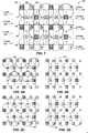
- FIG. 1 illustrates a virtual pixel to physical LED mapping on an array of LEDs 100 for one or more embodiments of the present invention.
- pixels may include different discrete color sub-pixels for generating a merged pixel that appears as almost any color in the visible spectrum. Different colors may be merged to generate a color pixel.
- a common combination of discrete colors is to use red, green, and blue elements to generate a merged color pixel.
- LED display boards described herein mostly merge the colors from red LEDs, green LEDs, and blue LEDs to form color pixels.
- the descriptions herein generally describe three LEDs, one each of red, green, and blue to form a pixel.
- other embodiments may include multiple LEDs of some colors, such as, for example, one red LED, one blue LED, and two green LEDs.
- FIG. 1 illustrates interleaved rows of LEDs as odd LED rows (P-ODD, 110) and even LED rows (P-EVEN, 120).
- the LEDs in the odd LED rows 110 are arranged in a repeating pattern of red LEDs 102, green LEDs 104, and blue LEDs 106.
- the LEDs in the even LED rows 120 are arranged in a repeating pattern of red LEDs 102, green LEDs 104, and blue LEDs 106.
- the LEDs in the even LED rows 120 are offset (i.e., staggered) relative to the LEDs in the odd LED rows 110 such that each LED in the even LED rows 120 is about midway between neighboring pixels in neighboring odd LED rows 110.
- a blue LED 106 in any given even LED row 110 is about midway between the neighboring red LED 102 and the neighboring green LED 104 in the odd LED row 110 above and the odd LED row 110 below the even LED row 120.
- One aspect of the present invention is to present visual content with an apparent resolution that is higher than the actual resolution of the array of LEDs 100. This increased apparent resolution is accomplished by sharing physical LEDs between different virtual pixels in different frames of the visual content.
- each pixel includes a dedicated red sub-pixel, a dedicated green sub-pixel, and a dedicated blue sub-pixel.
- visual content that has 1280 pixels by 720 pixels for a total of 921,600 pixels would require three time that many sub-pixels (i.e., 2,764,800 sub-pixels).
- providing so many LEDs can get very expensive.
- Embodiments of the present invention reduce the number of LEDs required by sharing sub-pixels, while still presenting images that are at or near in quality to displays with dedicated sub-pixels.
- FIG. 1 virtual pixels are shown as boxes with a number therein and positioned between three adjacent physical LEDs, which are encircled by a circle with a different line pattern for virtual pixels belonging to different frames.
- Each virtual pixel is presented during a specific frame of the visual content as represented by the number in the box for the virtual pixel.
- Frame rates may vary widely depending on the type of visual content to be presented. Some non-limiting examples for frame rates are 5, 10, 15, 24, 30, 60, and 72 frames/second.
- FIGS. 2A-2D illustrate individual frame virtual pixels for the mapping of FIG. 1.
- FIG. 2A illustrates the first virtual pixels 132 of the first frame and their mapping to physical LEDs.
- FIG. 2B illustrates the second virtual pixels 134 of the second frame and their mapping to physical LEDs.
- FIG. 2C illustrates the third virtual pixels 136 of the third frame and their mapping to physical LEDs.
- FIG. 2D illustrates the fourth virtual pixels 138 of the fourth frame and their mapping to physical LEDs.
- first virtual pixels 132 are in odd virtual rows (V-ODD, 130)
- second virtual pixels 134 are in odd virtual rows 130
- third virtual pixels 136 are in even virtual rows (V-EVEN, 140)
- fourth virtual pixels 138 are in even virtual rows 120.
- First virtual pixels 132 and second virtual pixels 134 alternate in the odd virtual rows 130.
- third virtual pixels 136 and fourth virtual pixels 138 alternate in the even virtual rows 120.
- odd virtual rows 130 are displayed with first virtual pixels 132.
- odd virtual rows 130 are displayed with second virtual pixels 134.
- even virtual rows 140 are displayed with third virtual pixels 136.
- even virtual rows 140 are displayed with fourth virtual pixels 138.
- each physical LED in the odd LED rows 110 gets mapped to a virtual pixel in each of the four virtual frames. For example, looking at the middle odd LED row 110, each LED is circled by virtual pixels from each of the four frames.
- each physical LED in the even LED rows 120 gets mapped to a virtual pixel in two out of the four virtual frames.
- the first blue LED is used in frames 1 and 3
- the first red LED is used in frames 2 and 4
- the first green LED is used in frames 1 and 3
- the second blue LED is used in frames 2 and 4.
- control logic for an LED display board may occasionally change the definition of even rows and odd rows to better balance the usage of the LEDs.
- odd and even for both the physical LED rows and the virtual rows is completely arbitrary. For example, an array may start with a row number zero and would therefore have the first row as an even row, whereas an array starting with a row number one would have the first row as an odd row.
- the virtual pixels include LEDs from the odd and even physical rows with a repeating pattern including a pixel of R B G , a pixel of B G R , and a pixel of G B R .
- the virtual pixels include LEDs from the odd and even physical rows with a repeating pattern including a pixel of R B G, a pixel of B G R, and a pixel of G B R.
- FIG. 3 illustrates another virtual pixel to physical LED mapping on an LED display board for one or more embodiments of the present invention.
- the physical LED layout is the same as that of FIG. 1 .
- the mapping of virtual pixels onto these physical LEDs is different.
- FIGS. 4A-4D illustrate individual frame virtual pixels for the mapping of FIG. 3.
- FIG. 4A illustrates the first virtual pixels 232 of the first frame and their mapping to physical LEDs.
- FIG. 4B illustrates the second virtual pixels 234 of the second frame and their mapping to physical LEDs.
- FIG. 4C illustrates the third virtual pixels 236 of the third frame and their mapping to physical LEDs.
- FIG. 4D illustrates the fourth virtual pixels 238 of the fourth frame and their mapping to physical LEDs.
- first virtual pixels 232 are in odd virtual rows (V-ODD, 230)
- second virtual pixels 234 are in odd virtual rows 230
- third virtual pixels 236 are in even virtual rows (V-EVEN, 220)
- fourth virtual pixels 238 are in even virtual rows 220.
- First virtual pixels 232 and second virtual pixels 234 alternate in the odd virtual rows 230.
- third virtual pixels 236 and fourth virtual pixels 238 alternate in the even virtual rows 220.
- odd virtual rows 230 are displayed with first virtual pixels 232.
- odd virtual rows 230 are displayed with second virtual pixels 234.
- even virtual rows 240 are displayed with third virtual pixels 236.
- even virtual rows 240 are displayed with fourth virtual pixels 138.
- the virtual pixels are mapped to different physical LEDs.
- One noticeable characteristic of this virtual pixel to physical LED mapping is the usage of the physical LEDs.
- Each physical LED in the odd LED rows 110 gets mapped to a virtual pixel in each three of the four frames. For example, looking at the middle odd LED row 110, the first blue LED is circled by a virtual pixel from each of frames 1, 2, and 4. The first red LED is circled by a virtual pixel from each of frames 1, 2, and 3. The second green LED is circled by a virtual pixel from each of frames 1, 2, and 4.
- each physical LED in the even LED rows 120 gets mapped to a virtual pixel in three of the four virtual frames.
- the first red LED is circled by a virtual pixel from each of frames 2, 3, and 4.
- the first green LED is circled by a virtual pixel from each of frames 1, 3, and 4.
- the second blue LED is circled by a virtual pixel from each of frames 2, 3, and 4.
- the virtual pixels include LEDs from the odd and even physical rows with a repeating pattern including a pixel of R B G , a pixel of B G R , and a pixel of G B R .
- the virtual pixels include LEDs from the odd and even physical rows with a repeating pattern including a pixel of R B G , a pixel of B G R , and a pixel of
- FIG. 5 illustrates various formats for visual content that may be used when processing the visual content for presentation on an LED display board.
- An input image (310A or 310B) may be scaled such that the pixel layout and aspect ratio of the input image (310A or 310B) matches that of the array of virtual pixels 340 to be presented on the LED display board.
- a smaller input image 310B may be scaled up and a larger input image 310A may be scaled down to match the array of virtual pixels 340. This scaling process may not be necessary if the sizes already match.
- the scaling may be any scaling algorithm, such as, for example, dropping pixels as a simple process to a high-quality bicubic scaling for a more complex process.
- the output of the scaling process is an input canvas image 320.
- the input canvas image 320 may be processed to develop an output canvas image 330 by blending color information from various neighboring pixels as explained with reference to FIGS. 6A-6F .
- the output canvas image 330 contains the array of virtual pixels 340 that are to be mapped to the physical LEDs on the LED display board.
- both the input canvas image 330 and the output canvas image 330 have enough detail (i.e., size) to allow for mapping of physical LED element positions that are spaced correctly relative to each other as they are on the actual LED display board.
- FIGS. 6A-6F illustrates example pixel layouts that may be used to blend neighboring pixels with a specific pixel, which may produce a more visually pleasing result.
- pixel blending may produce a more pleasing image on the display.
- content containing streaming video may benefit from one type of blending
- content containing text may benefit from another type of blending.
- one type of blending may produce better results for a given virtual pixel to physical LED mapping than a different virtual to physical mapping.
- the visual content may include segments that contain text using one type of blending and other segments that contain video streams using a different type of blending.
- the pixel with the circle is a subject pixel and a pixel with an "X" is a blending pixel used in the blending.
- the blending process takes the intensity for each color of the subject pixel and blends intensity for each color of each of the blending pixels to create an output canvas image pixel at the subject pixel location.
- Each blending pixel may be assigned a different weighting when it is combined with the subject pixel to accomplish different effects and possibly give more weight to blending pixels that are nearer to the subject pixel.
- the process is repeated using each pixel of the input canvas image as a subject pixel to create the entire array of virtual pixels in the output canvas image.
- FIG. 6A illustrates an H map 352 wherein neighboring pixels on each side of the subject pixel are used as blending pixels.
- the H pattern may be extended up, down, or a combination thereof to include additional blending pixels.
- FIG. 6B illustrates an I map 354 wherein neighboring pixels on a top side and a bottom side of the subject pixel are used as blending pixels.
- the I pattern may be extended to one side or both sides to include additional blending pixels.
- FIG. 6C illustrates an X map 356 wherein neighboring pixels on the corners of the subject pixel are used as blending pixels.
- the X pattern may be extended out away from the subject pixel to include additional blending pixels.
- FIG. 6D illustrates a cross map 358 wherein neighboring pixels on a top side, a bottom side, a left side and a right side of the subject pixel are used as blending pixels.
- the cross pattern may be extended out away from the subject pixel to include additional blending pixels.
- FIG. 6E illustrates an oval map 360, which pulls data from all blending pixels within an oval 380 about the subject pixel.
- the oval may be of varying size (i.e., encompassing a varying number of neighboring pixels) and, of course, may be considered a circle if both axes of the oval are the same length.
- FIG. 6F illustrates a rectangle map 362, which pulls data from all blending pixels within a rectangle about the subject pixel.
- the rectangle may be of varying size and, of course, may be considered a square if both axes of the rectangle are the same length.
- FIG. 7 is a simplified flow chart showing a process 400 of mapping an input image to physical LED placements on an LED display board.
- an input frame may be scaled to match a virtual resolution of the LED display board.
- An input canvas image 320 is generated as a result of the scaling.
- the input canvas image 320 may be processed to blend pixels with one of the maps discussed above with reference to FIGS. 6A-6F .
- An output canvas image 330 is generated from the blending process.
- the pixels of the output canvas image 330 may be mapped to the physical LEDs for the current frame of four frames as discussed above with respect to FIGS. 1-4D to generate an output image.
- human perception may tend to integrate the pixels from temporally adjacent frames. As a result, multiple frames of still images tend to appear as smooth motion. Since this integration may be naturally performed by human perception, some embodiments of the present invention may take advantage of this perception by combining multiple subsequent frames together and displaying the frames less often.
- an input frame rate may be 60 frames/second, such that a group of four frames is displayed at a rate of 15 groups per second.
- some embodiments of the present invention may rasterize an individual frame to the display 60 times per second, combine every two temporally adjacent frames and rasterize the combined frames to the display 30 times per second, or combine four temporally adjacent frames and rasterize the combined frames to the display 15 time per second.
- embodiments of the present invention may include other frame rates and other numbers of frames to be combined.
- the combination of temporally adjacent frames may be as simple as averaging the intensity values for each pixel from each frame to be combined. Other combinations may use more complex weighted averages for each of the corresponding pixels from different frames.
- a frame to be displayed may combine multiple temporally adjacent frames such that there is an overlap of input frames relative to output frames.
- an output frame may use a weighted average of four temporally adjacent input frames, yet the output frames are rasterized at one-half the frame rate of the input frames.
- each pixel of an output frame may include: 1 ⁇ 4F1 +1 ⁇ 2F2 +1 ⁇ 2 F3 +1 ⁇ 4F4.
- F1-F4 are four temporally adjacent input frames.
- the next output frame may include 1 ⁇ 4F3 + 1 ⁇ 2F4 +1 ⁇ 2 F5 +1 ⁇ 4F6.
- this is just one example of many types of temporal combinations and weightings that may be performed on the input images to reduce the frame rate on the actual output while maintaining an apparently higher frame rate to human perception.
- decision block 408 determines if temporally adjacent frames are going to be combined. If so, operation block 410 combines the current frame with one or more previous frames, as discussed above.
- Decision block 412 determines if a frame should be displayed on this time through the loop of display frames. In other words, as some examples, if the output frame rate were to match the input frame rate, decision block 412 would evaluate true every time through the loop. If the output frame rate were to be one-half the input frame rate, decision block 412 would evaluate true every other time through the loop. If the output frame rate were to be one-fourth the input frame rate, decision block 412 would evaluate true every fourth time through the loop.
- the output image for the current display frame or the combined display frame is rasterized to the LEDs of the display board depending on whether a combined display frame has been generated.
- Decision block 416 tests to see if the last frame of the four frames for the current input frame has been processed. If not, operation block 418 sets the next display frame and the process loops through operations 406 through 414 to determine and rasterize the next frame of the output image. If the last frame of the four frames for the current input frame has been processed, operation block 420 points to the next input frame and the process 400 repeats for the new input frame.
- the scaling process of operation block 402 may not need to be performed.
- the blending process of operation block 404 may not be desired, or may only be performed on portions of the input canvas image.
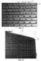
- FIGS. 8A-8C show portions of an LED display board showing placement of various colors of LEDs and edges of LED display boards and removable panels.
- FIG. 8A shows a portion of an LED display board 190 showing placement of various colors of LEDs, such as red LEDs 102, green LEDs 104, and blue LEDs 106. Also shown are driver integrated circuits 195 that may be used to drive and control LEDs near the driver integrated circuit 195.
- FIG. 8B shows portions of two LED display boards (190-1 and 190-2) to shown corrugated edges (195-1 and 195-2) that are abutted together when the LED display boards (190-1 and 190-2) are combined to create a large display.
- the corrugated edges (195-1 and 195-2) include alternating ridges (198-1 and 198-2) and furrows (197-1 and 197-2). These corrugated edges (195-1 and 195-2) are configured such that an LED may be positioned in the ridges.
- blue LEDs 196-2 are positioned in the ridges 198-2 of the second LED display board 190-2 (also referred to herein as even LED display boards).
- green LEDs 198-1 are positioned in the ridges 198-1 of the first LED display board 190-1 (also referred to herein as odd LED display boards).
- red LEDs (192-1 and 192-2) are positioned in the furrows of both the odd LED display boards 190-1 and the even LED display boards 190-2).
- FIG. 8C shows portions of two removable panels (512-1 and 512-2) to shown panel corrugated edges (540-1 and 540-2) that are abutted together when the removable panels (512-1 and 512-2) are combined to create a large display. Additional details of the removable panels are described below with reference to FIGS. 9-12 .
- the panel corrugated edges (540-1 and 540-2) include alternating ridges and furrows in a manner similar to the LED display boards (190-1 and 190-2) of FIG. 8B .
- the removable panels (512-1 and 512-2) are configured to accept the LED display boards (190-1 and 190-2) such that the LEDs protrude through the apertures 520 in the removable panels (512-1 and 512-2).
- the corrugated edges (195-1 and 195-2) on the LED display boards, and the panel corrugated edges (540-1 and 540-2) are configured such that pixel spacing between boards maintains the same distances as the pixel spacing within boards when the removable panels (512-1 and 512-2) including the LED display boards (190-1 and 190-2) are abutted.
- FIGS. 8B and 8C show the corrugated edges of ridges and furrows comprised of angled edges.
- the corrugated edges may comprise rectilinear teeth that are configured to mesh together or undulating curves that are configured to mesh together.
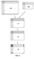
- FIG. 9 illustrates a simplified view of plurality of removable panels arranged in a matrix organization.
- An electronic display 500 (such as an LED display board) may include a single display module 510, or, as illustrated in FIGS. 9 and 10 , an electronic display 500 may include a plurality of display modules 510 arranged in a matrix organization. Additionally, these display modules 510 may be arranged in a variety of configurations for different applications.
- the matrix organization may include a single row of display modules 510 (or a single column of display modules 510) for creating a narrow yet long display, which may be suitable for displaying messages in a traveling ticker-tape type of arrangement.
- a small number of display modules 510 may be used to create a relatively small electronic display 500, or a large number of display modules 510 may be arranged to create a relatively large electronic display 500.
- a relatively large billboard size electronic display 500 may include a matrix organization of 1100 or more display modules 510 in a rectangular configuration. Additionally, using a plurality of display modules 510 to form a larger electronic display 500 may allow for the easier maintenance, installation, and removal of the electronic display 500. For example, each display module 510 of the electronic display 500 may be readily removed and replaced.
- FIG. 10 illustrates an exploded view of removable panels for attachment to frame members 550.
- a plurality of display modules 510 may be attached to frame members 550 as part of the electronic display 500.
- the frame members 550 may extend vertically and each module 510 may be placed in a removable panel position such that it abuts a neighboring display module 510 horizontally.
- the display modules 510 also may be stacked vertically to form the overall electronic display 500 for presenting the visual content.
- the overall electronic display 500 may be configured to display visual content, such as for example, a series of still images, or a video image.
- each display module 510 may be configured to form only a relatively small portion of the overall visual content.
- Each display module 510 ( FIG. 10 ) includes a removable panel 512, as shown in FIGS. 11 and 12.
- FIG. 11 illustrates a front view of an embodiment of removable panel 512 for a display module 510
- FIG. 12 illustrates a perspective view of the removable panel 512 shown in FIG. 11 .
- Each display module 512 includes one or more pixel rows 514 comprising a plurality of pixel arrangements 530 positioned and configured to display at least a portion of the visual content.
- the removable panel 512 may further comprise horizontal fins 540.
- Each pixel row 514 may include a plurality of pixel arrangements 530, and each pixel arrangement 530 may include one or more apertures 520.
- each pixel arrangement 530 may include two apertures 520 for receiving LEDs on a display board 190 as shown in FIG. 8 .
- the removable panel 512 is illustrated with a plurality of pixel rows 514. However, the removable panel 512 also may be formed having only a single pixel row 514. Additionally, the removable panel 512 may be formed having any number of pixel arrangements 530 and may include different pixel row geometries as well as different overall geometries.
- Electronic displays 500 may take on a number of forms and formats.
- electronic displays 500 may be in the form of billboards, displays on busses, displays on bus shelters, mall directory signs, airport signs, signs in sporting and other event arenas, signs on taxis, and any other place where displays are used for advertising.
- the visual content to be presented on the displays may be formatted in any suitable format for presenting and transmitting video, still-images, and text.
- some of the formats may include ASCII text, graphic interchange formats (GIF), bitmap (BMP) formats, Joint Photographic Experts Group (JPEG) formats, Moving Picture Experts Group (MPEG) formats, and the like.
- the visual content may include animations, Really Simple Syndication (RSS) feeds, web pages, time of day, temperature, stock quotes, emergency information, extensible Markup Language (XML) files, data files, Hyper-Text Markup Language (HTML) files, and combinations thereof.
- RSS Really Simple Syndication
- the electronic displays 500 may include audio content through an audio output (not shown).
- the audio content may be formatted in any suitable format for presenting and transporting audio.
- some of the formats may include MPEG-3 (MP3), wave (WAV) windows media audio (WMA), Advanced Audio Coding (AAC), and the like.
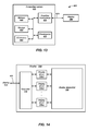
- FIG. 13 is a simplified block diagram of a display system 600 including a computing system 610 and a display 700 coupled to the computing system 610.
- the computing system 610 is configured for executing software programs containing computing instructions and includes one or more processors 620.
- the computing system 610 may also include memory 640, storage 650, one or more Input/Output (I/O) elements 660, and one or more graphics controllers 630.
- I/O Input/Output
- the one or more processors 620 may be configured for executing a wide variety of operating systems and applications including computing instructions for carrying out embodiments of the present invention.
- the memory 640 may be used to hold computing instructions, data, and other information for performing a wide variety of tasks including performing embodiments of the present invention.
- the memory 640 may include Synchronous Random Access Memory (SRAM), Dynamic RAM (DRAM), Read-Only Memory (ROM), Flash memory, and the like.
- the storage 650 may be used for storing large amounts of non-volatile information for use in the display system 600 and may be configured as one or more storage devices.
- these storage devices may include computer-readable media (CRM).
- CRM may include, but is not limited to magnetic and optical storage devices such as disk drives, magnetic tapes, CDs (compact disks), DVDs (digital versatile discs or digital video discs), and other equivalent storage devices.
- the I/O elements 660 may be any suitable input output devices such as displays, keyboards, mice, and communication elements.
- the I/O elements 660 may be configured for communicating with other devices or communication networks.
- the I/O elements 660 may include elements for communicating on wired and wireless communication media, such as for example, serial ports, parallel ports, Ethernet connections, universal serial bus (USB) connections IEEE 1394 ("firewire") connections, bluetooth wireless connections, 802.1 a/b/g/n type wireless connections, and other suitable communication interfaces and protocols.
- a graphics communication bus 675 is operably coupled to the computing system 610.
- the graphics communication bus 675 may be used for sending control information from the computing system 610 to the display 700.
- graphical information may be communicated between the computing system 610 and the display 700 on the graphics communication bus 675 (also may be referred to herein as a display bus 675).
- the graphics communication bus 675 may be operably coupled with the graphics controller 630. However, in some embodiments there may not be a graphics controller 630 and the graphics control function may be performed by the processor 620. In still other embodiments, the graphics controller 630 may be embedded in the processor 620.
- the graphics communication bus 275 may be a Video Graphics Array (VGA) bus, a Digital Video Interface (DVI) bus, a High Definition Media Interface (HDMI) bus, a Serial Digital Interface (SDI) bus, or other communication bus suitable for transmitting graphical frame information.
- VGA Video Graphics Array
- DVI Digital Video Interface
- HDMI High Definition Media Interface
- SDI Serial Digital Interface
- computing instructions for performing the processes may be stored on the storage 650, transferred to the memory 640 for execution, and executed by the processor 620, the graphics controller 630, the display 700, or combinations thereof.
- some or all portions of the processes may be performed by hardware specifically configured for carrying out the processes.
- FIG. 14 is a simplified block diagram of a display 700 for use with the display system 600 of FIG. 13 .
- Each display 700 may include a controller 710, one or more display drivers (730-1 through 730-p), and one or more display elements 720.
- the display controller may be configured for receiving media content, determining which media content is for the display elements present on that display 700.
- the controller 710 may also include functions such as, for example, formatting the content for its electronic display 700, animating the content for its electronic display 700, controlling presentation of audio content on audio elements, controlling timing of various content on the display element 700, controlling timing of various content on the audio element, and communicating with the computing system 610.
- the display elements 720 may be configured as LED display boards 190 with LEDs, as shown in FIG. 8 . Furthermore, the display elements may be partitioned into sections, such that each section may be controlled by a separate display driver 730. As a non-limiting example, in FIG. 14 , display driver 730-1 may control an upper strip of the display elements 720, display driver 730-2 may control a middle strip of the display elements 720, and display driver 730-p may control a lower strip of the display elements 720.
- the segmentation may be in many different forms such as, for example, rectangular sections, horizontal strips, or vertical strips.
Landscapes
- Engineering & Computer Science (AREA)
- Theoretical Computer Science (AREA)
- Physics & Mathematics (AREA)
- General Physics & Mathematics (AREA)
- Computer Hardware Design (AREA)
- Multimedia (AREA)
- Human Computer Interaction (AREA)
- General Engineering & Computer Science (AREA)
- Control Of Indicators Other Than Cathode Ray Tubes (AREA)
- Control Of El Displays (AREA)
- Devices For Indicating Variable Information By Combining Individual Elements (AREA)
Applications Claiming Priority (1)
| Application Number | Priority Date | Filing Date | Title |
|---|---|---|---|
| US12/635,636 US8502758B2 (en) | 2009-12-10 | 2009-12-10 | Apparatus and method for mapping virtual pixels to physical light elements of a display |
Publications (3)
| Publication Number | Publication Date |
|---|---|
| EP2333760A2 true EP2333760A2 (fr) | 2011-06-15 |
| EP2333760A3 EP2333760A3 (fr) | 2012-05-02 |
| EP2333760B1 EP2333760B1 (fr) | 2019-07-31 |
Family
ID=43640147
Family Applications (1)
| Application Number | Title | Priority Date | Filing Date |
|---|---|---|---|
| EP10194581.4A Not-in-force EP2333760B1 (fr) | 2009-12-10 | 2010-12-10 | Appareil et procédé de cartographie de pixels virtuels sur les éléments lumineux physiques d'un écran |
Country Status (3)
| Country | Link |
|---|---|
| US (1) | US8502758B2 (fr) |
| EP (1) | EP2333760B1 (fr) |
| CA (1) | CA2724580C (fr) |
Cited By (8)
| Publication number | Priority date | Publication date | Assignee | Title |
|---|---|---|---|---|
| CN103903524A (zh) * | 2014-03-25 | 2014-07-02 | 京东方科技集团股份有限公司 | 显示方法 |
| CN103903549A (zh) * | 2014-03-25 | 2014-07-02 | 京东方科技集团股份有限公司 | 显示方法 |
| CN103915044A (zh) * | 2014-03-25 | 2014-07-09 | 京东方科技集团股份有限公司 | 显示方法 |
| CN103927946A (zh) * | 2014-03-25 | 2014-07-16 | 京东方科技集团股份有限公司 | 显示方法 |
| CN104680966A (zh) * | 2015-03-19 | 2015-06-03 | 京东方科技集团股份有限公司 | 一种显示装置的驱动方法及其驱动装置 |
| CN104732928A (zh) * | 2015-04-09 | 2015-06-24 | 京东方科技集团股份有限公司 | 一种像素结构、其驱动方法及显示装置 |
| CN114582270A (zh) * | 2020-11-30 | 2022-06-03 | 西安诺瓦星云科技股份有限公司 | 亮色度数据获取方法、装置及系统和计算机可读存储介质 |
| CN115631715A (zh) * | 2022-09-27 | 2023-01-20 | 长春希达电子技术有限公司 | 一种led显示屏校正方法 |
Families Citing this family (31)
| Publication number | Priority date | Publication date | Assignee | Title |
|---|---|---|---|---|
| CN102569593A (zh) * | 2010-12-22 | 2012-07-11 | 展晶科技(深圳)有限公司 | 发光二极管 |
| DE102012100426A1 (de) * | 2012-01-19 | 2013-07-25 | Osram Opto Semiconductors Gmbh | Anzeigevorrichtung und Verfahren zur Darstellung dreidimensionaler Bilder |
| US20150016104A1 (en) * | 2013-07-11 | 2015-01-15 | Everlight Electronics Co., Ltd. | Lighting Component And Lighting Device |
| US9736895B1 (en) | 2013-10-03 | 2017-08-15 | Ketra, Inc. | Color mixing optics for LED illumination device |
| US9277630B2 (en) * | 2013-11-08 | 2016-03-01 | Zachary Leonid Braunstein | Apparatus intelligent parallel view LED light, methods of configuration and controls |
| US20150187237A1 (en) | 2013-12-31 | 2015-07-02 | Ultravision Holdings, Llc | System and Method for a Modular Multi-Panel Display |
| US9582237B2 (en) | 2013-12-31 | 2017-02-28 | Ultravision Technologies, Llc | Modular display panels with different pitches |
| US9195281B2 (en) | 2013-12-31 | 2015-11-24 | Ultravision Technologies, Llc | System and method for a modular multi-panel display |
| US9416551B2 (en) | 2013-12-31 | 2016-08-16 | Ultravision Technologies, Llc | Preassembled display systems and methods of installation thereof |
| CN104050896A (zh) * | 2014-05-19 | 2014-09-17 | 京东方科技集团股份有限公司 | 一种显示面板及其显示方法和显示装置 |
| US10706770B2 (en) | 2014-07-16 | 2020-07-07 | Ultravision Technologies, Llc | Display system having module display panel with circuitry for bidirectional communication |
| CN104240195B (zh) * | 2014-08-20 | 2017-01-18 | 京东方科技集团股份有限公司 | 一种基于虚拟算法的模型建立方法和系统 |
| CN104375302B (zh) * | 2014-10-27 | 2020-09-08 | 上海中航光电子有限公司 | 一种像素结构、显示面板及其像素补偿方法 |
| CN104835444B (zh) | 2015-06-05 | 2017-07-14 | 京东方科技集团股份有限公司 | 一种显示方法及显示装置 |
| CN104933980B (zh) * | 2015-06-30 | 2017-10-31 | 京东方科技集团股份有限公司 | 一种显示驱动方法、装置及显示装置 |
| CN105096885B (zh) * | 2015-08-28 | 2018-01-02 | 厦门天马微电子有限公司 | 阵列基板、显示装置及子像素渲染方法 |
| CN105489177B (zh) * | 2015-11-30 | 2018-06-29 | 信利(惠州)智能显示有限公司 | 子像素渲染方法及渲染装置 |
| CN107275359B (zh) | 2016-04-08 | 2021-08-13 | 乐金显示有限公司 | 有机发光显示装置 |
| WO2019058307A1 (fr) * | 2017-09-20 | 2019-03-28 | Imax Theatres International Limited | Affichage électroluminescent avec pavés et traitement de données |
| US20190213946A1 (en) * | 2017-10-18 | 2019-07-11 | Dongguan Darzune Optotech Co., Limited | Led module, led display screen, and display system |
| CN108230926A (zh) * | 2017-12-29 | 2018-06-29 | 西安智盛锐芯半导体科技有限公司 | 基于四色led芯片的虚拟led显示模组及4倍频显示方法 |
| CN110137209A (zh) * | 2018-02-09 | 2019-08-16 | 京东方科技集团股份有限公司 | 一种像素排布结构、高精度金属掩模板及显示装置 |
| FR3081251B1 (fr) * | 2018-05-16 | 2020-06-05 | Microoled | Dispositif d'affichage permettant de traiter un double signal d'entree |
| CN109451150A (zh) * | 2018-10-22 | 2019-03-08 | 南昌黑鲨科技有限公司 | 灯效控制方法、控制单元、智能终端及计算机可读存储介质 |
| CN113823240B (zh) * | 2018-12-13 | 2023-04-18 | 京东方科技集团股份有限公司 | 显示装置 |
| DE102019109137A1 (de) | 2019-04-08 | 2020-10-08 | OSRAM Opto Semiconductors Gesellschaft mit beschränkter Haftung | Bauelement für eine anzeigevorrichtung, anzeigevorrichtung und verfahren zum betreiben der anzeigevorrichtung |
| CN112038375B (zh) * | 2020-09-02 | 2022-11-15 | 昆山国显光电有限公司 | 显示面板和显示装置 |
| CN113362214B (zh) * | 2021-06-07 | 2024-10-22 | 上海新相微电子股份有限公司 | 基于虚拟像素阵列生成的图像自生成系统 |
| CN114093312B (zh) * | 2021-11-26 | 2023-03-31 | 卡莱特云科技股份有限公司 | 一种基于虚拟像素的显示数据生成方法及装置 |
| CN114582280B (zh) * | 2022-05-05 | 2022-08-05 | 卡莱特云科技股份有限公司 | 基于奇偶显示的显示屏对比度提升方法、装置及电子设备 |
| CN115132133B (zh) * | 2022-08-31 | 2022-11-18 | 长春希达电子技术有限公司 | 像素倍增显示屏的数据传输系统、控制系统、方法和装置 |
Family Cites Families (27)
| Publication number | Priority date | Publication date | Assignee | Title |
|---|---|---|---|---|
| EP0717878A1 (fr) | 1994-06-30 | 1996-06-26 | Koninklijke Philips Electronics N.V. | Dispositif d'affichage |
| US5949581A (en) * | 1997-08-12 | 1999-09-07 | Daktronics, Inc. | Display system |
| DE19746329A1 (de) | 1997-09-13 | 1999-03-18 | Gia Chuong Dipl Ing Phan | Display und Verfahren zur Ansteuerung des Displays |
| US7215347B2 (en) | 1997-09-13 | 2007-05-08 | Gia Chuong Phan | Dynamic pixel resolution, brightness and contrast for displays using spatial elements |
| US7091986B2 (en) | 1997-09-13 | 2006-08-15 | Gia Chuong Phan | Dynamic pixel resolution, brightness and contrast for displays using spatial elements |
| US6950115B2 (en) | 2001-05-09 | 2005-09-27 | Clairvoyante, Inc. | Color flat panel display sub-pixel arrangements and layouts |
| US7274383B1 (en) | 2000-07-28 | 2007-09-25 | Clairvoyante, Inc | Arrangement of color pixels for full color imaging devices with simplified addressing |
| US7283142B2 (en) | 2000-07-28 | 2007-10-16 | Clairvoyante, Inc. | Color display having horizontal sub-pixel arrangements and layouts |
| JP3852561B2 (ja) * | 2001-03-21 | 2006-11-29 | 三菱電機株式会社 | 画像表示装置および画像表示方法 |
| TW540022B (en) | 2001-03-27 | 2003-07-01 | Koninkl Philips Electronics Nv | Display device and method of displaying an image |
| US7123277B2 (en) | 2001-05-09 | 2006-10-17 | Clairvoyante, Inc. | Conversion of a sub-pixel format data to another sub-pixel data format |
| US7307646B2 (en) | 2001-05-09 | 2007-12-11 | Clairvoyante, Inc | Color display pixel arrangements and addressing means |
| KR20040052246A (ko) | 2001-10-19 | 2004-06-22 | 코닌클리케 필립스 일렉트로닉스 엔.브이. | 컬러 영상을 디스플레이하기 위한 방법 및 디스플레이처리 유닛 및 그러한 디스플레이 처리 유닛을 포함하는디스플레이 장치 |
| US7417648B2 (en) | 2002-01-07 | 2008-08-26 | Samsung Electronics Co. Ltd., | Color flat panel display sub-pixel arrangements and layouts for sub-pixel rendering with split blue sub-pixels |
| US7492379B2 (en) | 2002-01-07 | 2009-02-17 | Samsung Electronics Co., Ltd. | Color flat panel display sub-pixel arrangements and layouts for sub-pixel rendering with increased modulation transfer function response |
| TW559763B (en) | 2002-09-11 | 2003-11-01 | Neo Led Technology Co Ltd | High resolution driving method of full-color LED display board |
| JP2004145156A (ja) | 2002-10-28 | 2004-05-20 | Nippon Hoso Kyokai <Nhk> | 画像表示パネル |
| US6867549B2 (en) | 2002-12-10 | 2005-03-15 | Eastman Kodak Company | Color OLED display having repeated patterns of colored light emitting elements |
| US7352374B2 (en) | 2003-04-07 | 2008-04-01 | Clairvoyante, Inc | Image data set with embedded pre-subpixel rendered image |
| US7209105B2 (en) | 2003-06-06 | 2007-04-24 | Clairvoyante, Inc | System and method for compensating for visual effects upon panels having fixed pattern noise with reduced quantization error |
| US7355562B2 (en) | 2004-02-17 | 2008-04-08 | Thomas Schubert | Electronic interlocking graphics panel formed of modular interconnecting parts |
| US20060055642A1 (en) | 2004-09-16 | 2006-03-16 | Billboard Video, Inc. | LED display modules with pixel designs for enhanced visual quality of virtual pixels |
| KR100688801B1 (ko) * | 2004-11-22 | 2007-03-02 | 삼성에스디아이 주식회사 | 델타 화소회로 및 발광 표시장치 |
| JP4777675B2 (ja) | 2005-03-17 | 2011-09-21 | 株式会社リコー | 画像処理装置、画像表示装置、画像処理方法、その方法をコンピュータに実行させるプログラム、および記録媒体 |
| US7907133B2 (en) | 2006-04-13 | 2011-03-15 | Daktronics, Inc. | Pixel interleaving configurations for use in high definition electronic sign displays |
| US8111208B2 (en) * | 2006-06-06 | 2012-02-07 | Young Electric Sign Company | Front and rear removable panel for electronic displays |
| US7682043B2 (en) * | 2007-07-05 | 2010-03-23 | Tyco Electronics Corporation | Wirelessly controlled light emitting display system |
-
2009
- 2009-12-10 US US12/635,636 patent/US8502758B2/en active Active
-
2010
- 2010-12-09 CA CA2724580A patent/CA2724580C/fr active Active
- 2010-12-10 EP EP10194581.4A patent/EP2333760B1/fr not_active Not-in-force
Cited By (18)
| Publication number | Priority date | Publication date | Assignee | Title |
|---|---|---|---|---|
| US9875682B2 (en) | 2014-03-25 | 2018-01-23 | Boe Technology Group Co., Ltd. | Display method and display panel |
| CN103915044A (zh) * | 2014-03-25 | 2014-07-09 | 京东方科技集团股份有限公司 | 显示方法 |
| CN103927946A (zh) * | 2014-03-25 | 2014-07-16 | 京东方科技集团股份有限公司 | 显示方法 |
| CN103903524B (zh) * | 2014-03-25 | 2016-06-15 | 京东方科技集团股份有限公司 | 显示方法 |
| CN103915044B (zh) * | 2014-03-25 | 2016-03-30 | 京东方科技集团股份有限公司 | 显示方法 |
| CN103927946B (zh) * | 2014-03-25 | 2016-06-08 | 京东方科技集团股份有限公司 | 显示方法 |
| CN103903549A (zh) * | 2014-03-25 | 2014-07-02 | 京东方科技集团股份有限公司 | 显示方法 |
| US10325539B2 (en) | 2014-03-25 | 2019-06-18 | Boe Technology Group Co., Ltd. | Display method, display panel and display device |
| CN103903549B (zh) * | 2014-03-25 | 2016-08-17 | 京东方科技集团股份有限公司 | 显示方法 |
| US10140902B2 (en) | 2014-03-25 | 2018-11-27 | Boe Technology Group Co., Ltd. | Display method and display panel |
| CN103903524A (zh) * | 2014-03-25 | 2014-07-02 | 京东方科技集团股份有限公司 | 显示方法 |
| US9959799B2 (en) | 2015-03-19 | 2018-05-01 | Boe Technology Group Co., Ltd. | Driving method and driving apparatus for display apparatus |
| CN104680966A (zh) * | 2015-03-19 | 2015-06-03 | 京东方科技集团股份有限公司 | 一种显示装置的驱动方法及其驱动装置 |
| CN104732928A (zh) * | 2015-04-09 | 2015-06-24 | 京东方科技集团股份有限公司 | 一种像素结构、其驱动方法及显示装置 |
| CN104732928B (zh) * | 2015-04-09 | 2017-05-24 | 京东方科技集团股份有限公司 | 一种像素结构、其驱动方法及显示装置 |
| US9653017B2 (en) | 2015-04-09 | 2017-05-16 | Boe Technology Group Co., Ltd. | Pixel structure, driving method thereof and display device |
| CN114582270A (zh) * | 2020-11-30 | 2022-06-03 | 西安诺瓦星云科技股份有限公司 | 亮色度数据获取方法、装置及系统和计算机可读存储介质 |
| CN115631715A (zh) * | 2022-09-27 | 2023-01-20 | 长春希达电子技术有限公司 | 一种led显示屏校正方法 |
Also Published As
| Publication number | Publication date |
|---|---|
| CA2724580C (fr) | 2017-06-27 |
| EP2333760A3 (fr) | 2012-05-02 |
| US8502758B2 (en) | 2013-08-06 |
| US20110140999A1 (en) | 2011-06-16 |
| CA2724580A1 (fr) | 2011-06-10 |
| EP2333760B1 (fr) | 2019-07-31 |
Similar Documents
| Publication | Publication Date | Title |
|---|---|---|
| CA2724580C (fr) | Appareil et procede pour la mise en correspondance de pixels virtuels avec les elements lumineux materiels d'un affichage | |
| US9563910B2 (en) | Showcase system having transparent display panel and operating method thereof | |
| CN102903318B (zh) | 显示器的子像素排列及其呈现方法 | |
| CN101593469B (zh) | 不同密度像素点构成的led显示屏及其显示方法 | |
| US20110196749A1 (en) | Method for dynamic banner composition | |
| US20170117334A1 (en) | Array substrate and display device | |
| CA2703800C (fr) | Appareil et procede de commande de multiples dispositifs d'affichage | |
| KR102585233B1 (ko) | 디스플레이 장치 및 디스플레이 장치의 제조 방법 | |
| US20220019397A1 (en) | Signage device and method for controlling same | |
| US20170206854A1 (en) | Device and method for displaying information on a screen arrangement having a plurality of individual screen modules | |
| CN103745665A (zh) | 一种透明显示装置 | |
| CN103761315A (zh) | 一种显示网页内容的方法及系统 | |
| CN110262764A (zh) | 一种实现led显示屏视频播放的方法和装置以及设备 | |
| KR20160106970A (ko) | 디지털 사이니지의 최적 템플릿 생성 방법 및 그 장치 | |
| KR101624085B1 (ko) | 6필드 분할 표출방식의 보간 픽셀로 해상도를 6배 향상시킨 led전광판 | |
| US9886883B2 (en) | Display apparatus and a method of operating the same | |
| ES3002963T3 (en) | Electronic shelf label system with sectional control of display content | |
| US20120113069A1 (en) | Display device and method of driving the same | |
| JP2008292588A (ja) | 有機elパッシブマトリックス素子の駆動装置 | |
| KR100958611B1 (ko) | 디스플레이 시스템 | |
| CN100353404C (zh) | 发光二极管全彩显示板的高分辨率驱动方法 | |
| US20120069001A1 (en) | Electronic album generating apparatus, stereoscopic image pasting apparatus, and methods and programs for controlling operation of same | |
| KR20070106006A (ko) | 리셋 이미지를 나타내는 전기영동 디스플레이 패널 | |
| KR20010010147A (ko) | 액정 프로젝터를 이용한 전광판시스템 | |
| US10825370B1 (en) | Systems and methods for updating pixel arrays |
Legal Events
| Date | Code | Title | Description |
|---|---|---|---|
| PUAI | Public reference made under article 153(3) epc to a published international application that has entered the european phase |
Free format text: ORIGINAL CODE: 0009012 |
|
| AK | Designated contracting states |
Kind code of ref document: A2 Designated state(s): AL AT BE BG CH CY CZ DE DK EE ES FI FR GB GR HR HU IE IS IT LI LT LU LV MC MK MT NL NO PL PT RO RS SE SI SK SM TR |
|
| AX | Request for extension of the european patent |
Extension state: BA ME |
|
| RIN1 | Information on inventor provided before grant (corrected) |
Inventor name: BROWN, BRENT W Inventor name: BELAND, GRAHAM N Inventor name: BROWN, CLIFFORD BRENT Inventor name: GOVER, JAMES BLAKE |
|
| PUAL | Search report despatched |
Free format text: ORIGINAL CODE: 0009013 |
|
| AK | Designated contracting states |
Kind code of ref document: A3 Designated state(s): AL AT BE BG CH CY CZ DE DK EE ES FI FR GB GR HR HU IE IS IT LI LT LU LV MC MK MT NL NO PL PT RO RS SE SI SK SM TR |
|
| AX | Request for extension of the european patent |
Extension state: BA ME |
|
| RIC1 | Information provided on ipc code assigned before grant |
Ipc: G09G 3/32 20060101AFI20120323BHEP Ipc: G06T 3/40 20060101ALI20120323BHEP Ipc: G09F 9/33 20060101ALI20120323BHEP Ipc: G06F 3/14 20060101ALI20120323BHEP Ipc: G09G 3/20 20060101ALI20120323BHEP |
|
| 17P | Request for examination filed |
Effective date: 20121102 |
|
| 17Q | First examination report despatched |
Effective date: 20140916 |
|
| RAP1 | Party data changed (applicant data changed or rights of an application transferred) |
Owner name: YESCO ELECTRONICS LLC |
|
| STAA | Information on the status of an ep patent application or granted ep patent |
Free format text: STATUS: EXAMINATION IS IN PROGRESS |
|
| GRAP | Despatch of communication of intention to grant a patent |
Free format text: ORIGINAL CODE: EPIDOSNIGR1 |
|
| STAA | Information on the status of an ep patent application or granted ep patent |
Free format text: STATUS: GRANT OF PATENT IS INTENDED |
|
| RIC1 | Information provided on ipc code assigned before grant |
Ipc: G09F 9/302 20060101ALI20190130BHEP Ipc: G09G 3/20 20060101ALI20190130BHEP Ipc: G09F 9/33 20060101ALI20190130BHEP Ipc: G06F 3/14 20060101ALI20190130BHEP Ipc: G06T 3/40 20060101ALI20190130BHEP Ipc: G09G 3/32 20160101AFI20190130BHEP |
|
| INTG | Intention to grant announced |
Effective date: 20190220 |
|
| RAP1 | Party data changed (applicant data changed or rights of an application transferred) |
Owner name: PRISMVIEW LLC |
|
| GRAS | Grant fee paid |
Free format text: ORIGINAL CODE: EPIDOSNIGR3 |
|
| GRAA | (expected) grant |
Free format text: ORIGINAL CODE: 0009210 |
|
| STAA | Information on the status of an ep patent application or granted ep patent |
Free format text: STATUS: THE PATENT HAS BEEN GRANTED |
|
| AK | Designated contracting states |
Kind code of ref document: B1 Designated state(s): AL AT BE BG CH CY CZ DE DK EE ES FI FR GB GR HR HU IE IS IT LI LT LU LV MC MK MT NL NO PL PT RO RS SE SI SK SM TR |
|
| REG | Reference to a national code |
Ref country code: CH Ref legal event code: EP Ref country code: GB Ref legal event code: FG4D |
|
| REG | Reference to a national code |
Ref country code: AT Ref legal event code: REF Ref document number: 1161749 Country of ref document: AT Kind code of ref document: T Effective date: 20190815 |
|
| REG | Reference to a national code |
Ref country code: IE Ref legal event code: FG4D |
|
| REG | Reference to a national code |
Ref country code: DE Ref legal event code: R096 Ref document number: 602010060258 Country of ref document: DE |
|
| REG | Reference to a national code |
Ref country code: NL Ref legal event code: MP Effective date: 20190731 |
|
| REG | Reference to a national code |
Ref country code: LT Ref legal event code: MG4D |
|
| REG | Reference to a national code |
Ref country code: AT Ref legal event code: MK05 Ref document number: 1161749 Country of ref document: AT Kind code of ref document: T Effective date: 20190731 |
|
| PG25 | Lapsed in a contracting state [announced via postgrant information from national office to epo] |
Ref country code: HR Free format text: LAPSE BECAUSE OF FAILURE TO SUBMIT A TRANSLATION OF THE DESCRIPTION OR TO PAY THE FEE WITHIN THE PRESCRIBED TIME-LIMIT Effective date: 20190731 Ref country code: NL Free format text: LAPSE BECAUSE OF FAILURE TO SUBMIT A TRANSLATION OF THE DESCRIPTION OR TO PAY THE FEE WITHIN THE PRESCRIBED TIME-LIMIT Effective date: 20190731 Ref country code: BG Free format text: LAPSE BECAUSE OF FAILURE TO SUBMIT A TRANSLATION OF THE DESCRIPTION OR TO PAY THE FEE WITHIN THE PRESCRIBED TIME-LIMIT Effective date: 20191031 Ref country code: LT Free format text: LAPSE BECAUSE OF FAILURE TO SUBMIT A TRANSLATION OF THE DESCRIPTION OR TO PAY THE FEE WITHIN THE PRESCRIBED TIME-LIMIT Effective date: 20190731 Ref country code: FI Free format text: LAPSE BECAUSE OF FAILURE TO SUBMIT A TRANSLATION OF THE DESCRIPTION OR TO PAY THE FEE WITHIN THE PRESCRIBED TIME-LIMIT Effective date: 20190731 Ref country code: NO Free format text: LAPSE BECAUSE OF FAILURE TO SUBMIT A TRANSLATION OF THE DESCRIPTION OR TO PAY THE FEE WITHIN THE PRESCRIBED TIME-LIMIT Effective date: 20191031 Ref country code: AT Free format text: LAPSE BECAUSE OF FAILURE TO SUBMIT A TRANSLATION OF THE DESCRIPTION OR TO PAY THE FEE WITHIN THE PRESCRIBED TIME-LIMIT Effective date: 20190731 Ref country code: PT Free format text: LAPSE BECAUSE OF FAILURE TO SUBMIT A TRANSLATION OF THE DESCRIPTION OR TO PAY THE FEE WITHIN THE PRESCRIBED TIME-LIMIT Effective date: 20191202 Ref country code: SE Free format text: LAPSE BECAUSE OF FAILURE TO SUBMIT A TRANSLATION OF THE DESCRIPTION OR TO PAY THE FEE WITHIN THE PRESCRIBED TIME-LIMIT Effective date: 20190731 |
|
| PG25 | Lapsed in a contracting state [announced via postgrant information from national office to epo] |
Ref country code: LV Free format text: LAPSE BECAUSE OF FAILURE TO SUBMIT A TRANSLATION OF THE DESCRIPTION OR TO PAY THE FEE WITHIN THE PRESCRIBED TIME-LIMIT Effective date: 20190731 Ref country code: AL Free format text: LAPSE BECAUSE OF FAILURE TO SUBMIT A TRANSLATION OF THE DESCRIPTION OR TO PAY THE FEE WITHIN THE PRESCRIBED TIME-LIMIT Effective date: 20190731 Ref country code: IS Free format text: LAPSE BECAUSE OF FAILURE TO SUBMIT A TRANSLATION OF THE DESCRIPTION OR TO PAY THE FEE WITHIN THE PRESCRIBED TIME-LIMIT Effective date: 20191130 Ref country code: RS Free format text: LAPSE BECAUSE OF FAILURE TO SUBMIT A TRANSLATION OF THE DESCRIPTION OR TO PAY THE FEE WITHIN THE PRESCRIBED TIME-LIMIT Effective date: 20190731 Ref country code: ES Free format text: LAPSE BECAUSE OF FAILURE TO SUBMIT A TRANSLATION OF THE DESCRIPTION OR TO PAY THE FEE WITHIN THE PRESCRIBED TIME-LIMIT Effective date: 20190731 Ref country code: GR Free format text: LAPSE BECAUSE OF FAILURE TO SUBMIT A TRANSLATION OF THE DESCRIPTION OR TO PAY THE FEE WITHIN THE PRESCRIBED TIME-LIMIT Effective date: 20191101 |
|
| PG25 | Lapsed in a contracting state [announced via postgrant information from national office to epo] |
Ref country code: TR Free format text: LAPSE BECAUSE OF FAILURE TO SUBMIT A TRANSLATION OF THE DESCRIPTION OR TO PAY THE FEE WITHIN THE PRESCRIBED TIME-LIMIT Effective date: 20190731 |
|
| PG25 | Lapsed in a contracting state [announced via postgrant information from national office to epo] |
Ref country code: DK Free format text: LAPSE BECAUSE OF FAILURE TO SUBMIT A TRANSLATION OF THE DESCRIPTION OR TO PAY THE FEE WITHIN THE PRESCRIBED TIME-LIMIT Effective date: 20190731 Ref country code: PL Free format text: LAPSE BECAUSE OF FAILURE TO SUBMIT A TRANSLATION OF THE DESCRIPTION OR TO PAY THE FEE WITHIN THE PRESCRIBED TIME-LIMIT Effective date: 20190731 Ref country code: RO Free format text: LAPSE BECAUSE OF FAILURE TO SUBMIT A TRANSLATION OF THE DESCRIPTION OR TO PAY THE FEE WITHIN THE PRESCRIBED TIME-LIMIT Effective date: 20190731 Ref country code: IT Free format text: LAPSE BECAUSE OF FAILURE TO SUBMIT A TRANSLATION OF THE DESCRIPTION OR TO PAY THE FEE WITHIN THE PRESCRIBED TIME-LIMIT Effective date: 20190731 Ref country code: EE Free format text: LAPSE BECAUSE OF FAILURE TO SUBMIT A TRANSLATION OF THE DESCRIPTION OR TO PAY THE FEE WITHIN THE PRESCRIBED TIME-LIMIT Effective date: 20190731 |
|
| PG25 | Lapsed in a contracting state [announced via postgrant information from national office to epo] |
Ref country code: SM Free format text: LAPSE BECAUSE OF FAILURE TO SUBMIT A TRANSLATION OF THE DESCRIPTION OR TO PAY THE FEE WITHIN THE PRESCRIBED TIME-LIMIT Effective date: 20190731 Ref country code: IS Free format text: LAPSE BECAUSE OF FAILURE TO SUBMIT A TRANSLATION OF THE DESCRIPTION OR TO PAY THE FEE WITHIN THE PRESCRIBED TIME-LIMIT Effective date: 20200224 Ref country code: CZ Free format text: LAPSE BECAUSE OF FAILURE TO SUBMIT A TRANSLATION OF THE DESCRIPTION OR TO PAY THE FEE WITHIN THE PRESCRIBED TIME-LIMIT Effective date: 20190731 Ref country code: SK Free format text: LAPSE BECAUSE OF FAILURE TO SUBMIT A TRANSLATION OF THE DESCRIPTION OR TO PAY THE FEE WITHIN THE PRESCRIBED TIME-LIMIT Effective date: 20190731 |
|
| REG | Reference to a national code |
Ref country code: DE Ref legal event code: R097 Ref document number: 602010060258 Country of ref document: DE |
|
| REG | Reference to a national code |
Ref country code: DE Ref legal event code: R119 Ref document number: 602010060258 Country of ref document: DE |
|
| PLBE | No opposition filed within time limit |
Free format text: ORIGINAL CODE: 0009261 |
|
| STAA | Information on the status of an ep patent application or granted ep patent |
Free format text: STATUS: NO OPPOSITION FILED WITHIN TIME LIMIT |
|
| PG2D | Information on lapse in contracting state deleted |
Ref country code: IS |
|
| PG25 | Lapsed in a contracting state [announced via postgrant information from national office to epo] |
Ref country code: IS Free format text: LAPSE BECAUSE OF FAILURE TO SUBMIT A TRANSLATION OF THE DESCRIPTION OR TO PAY THE FEE WITHIN THE PRESCRIBED TIME-LIMIT Effective date: 20191030 |
|
| REG | Reference to a national code |
Ref country code: CH Ref legal event code: PL |
|
| 26N | No opposition filed |
Effective date: 20200603 |
|
| REG | Reference to a national code |
Ref country code: BE Ref legal event code: MM Effective date: 20191231 |
|
| PG25 | Lapsed in a contracting state [announced via postgrant information from national office to epo] |
Ref country code: SI Free format text: LAPSE BECAUSE OF FAILURE TO SUBMIT A TRANSLATION OF THE DESCRIPTION OR TO PAY THE FEE WITHIN THE PRESCRIBED TIME-LIMIT Effective date: 20190731 Ref country code: MC Free format text: LAPSE BECAUSE OF FAILURE TO SUBMIT A TRANSLATION OF THE DESCRIPTION OR TO PAY THE FEE WITHIN THE PRESCRIBED TIME-LIMIT Effective date: 20190731 |
|
| GBPC | Gb: european patent ceased through non-payment of renewal fee |
Effective date: 20191210 |
|
| PG25 | Lapsed in a contracting state [announced via postgrant information from national office to epo] |
Ref country code: GB Free format text: LAPSE BECAUSE OF NON-PAYMENT OF DUE FEES Effective date: 20191210 Ref country code: IE Free format text: LAPSE BECAUSE OF NON-PAYMENT OF DUE FEES Effective date: 20191210 Ref country code: LU Free format text: LAPSE BECAUSE OF NON-PAYMENT OF DUE FEES Effective date: 20191210 Ref country code: DE Free format text: LAPSE BECAUSE OF NON-PAYMENT OF DUE FEES Effective date: 20200701 |
|
| PG25 | Lapsed in a contracting state [announced via postgrant information from national office to epo] |
Ref country code: BE Free format text: LAPSE BECAUSE OF NON-PAYMENT OF DUE FEES Effective date: 20191231 Ref country code: LI Free format text: LAPSE BECAUSE OF NON-PAYMENT OF DUE FEES Effective date: 20191231 Ref country code: CH Free format text: LAPSE BECAUSE OF NON-PAYMENT OF DUE FEES Effective date: 20191231 |
|
| PG25 | Lapsed in a contracting state [announced via postgrant information from national office to epo] |
Ref country code: CY Free format text: LAPSE BECAUSE OF FAILURE TO SUBMIT A TRANSLATION OF THE DESCRIPTION OR TO PAY THE FEE WITHIN THE PRESCRIBED TIME-LIMIT Effective date: 20190731 |
|
| PG25 | Lapsed in a contracting state [announced via postgrant information from national office to epo] |
Ref country code: FR Free format text: LAPSE BECAUSE OF NON-PAYMENT OF DUE FEES Effective date: 20191231 Ref country code: MT Free format text: LAPSE BECAUSE OF FAILURE TO SUBMIT A TRANSLATION OF THE DESCRIPTION OR TO PAY THE FEE WITHIN THE PRESCRIBED TIME-LIMIT Effective date: 20190731 Ref country code: HU Free format text: LAPSE BECAUSE OF FAILURE TO SUBMIT A TRANSLATION OF THE DESCRIPTION OR TO PAY THE FEE WITHIN THE PRESCRIBED TIME-LIMIT; INVALID AB INITIO Effective date: 20101210 |
|
| PG25 | Lapsed in a contracting state [announced via postgrant information from national office to epo] |
Ref country code: MK Free format text: LAPSE BECAUSE OF FAILURE TO SUBMIT A TRANSLATION OF THE DESCRIPTION OR TO PAY THE FEE WITHIN THE PRESCRIBED TIME-LIMIT Effective date: 20190731 |