EP2336860A1 - Verbesserungen an - oder im Zusammenhang mit - optischen Navigationsgeräten - Google Patents
Verbesserungen an - oder im Zusammenhang mit - optischen Navigationsgeräten Download PDFInfo
- Publication number
- EP2336860A1 EP2336860A1 EP10194281A EP10194281A EP2336860A1 EP 2336860 A1 EP2336860 A1 EP 2336860A1 EP 10194281 A EP10194281 A EP 10194281A EP 10194281 A EP10194281 A EP 10194281A EP 2336860 A1 EP2336860 A1 EP 2336860A1
- Authority
- EP
- European Patent Office
- Prior art keywords
- navigation device
- optical navigation
- illumination
- operable
- reset
- Prior art date
- Legal status (The legal status is an assumption and is not a legal conclusion. Google has not performed a legal analysis and makes no representation as to the accuracy of the status listed.)
- Withdrawn
Links
Images

Classifications
-
- G—PHYSICS
- G06—COMPUTING OR CALCULATING; COUNTING
- G06F—ELECTRIC DIGITAL DATA PROCESSING
- G06F3/00—Input arrangements for transferring data to be processed into a form capable of being handled by the computer; Output arrangements for transferring data from processing unit to output unit, e.g. interface arrangements
- G06F3/01—Input arrangements or combined input and output arrangements for interaction between user and computer
- G06F3/03—Arrangements for converting the position or the displacement of a member into a coded form
- G06F3/041—Digitisers, e.g. for touch screens or touch pads, characterised by the transducing means
- G06F3/042—Digitisers, e.g. for touch screens or touch pads, characterised by the transducing means by opto-electronic means
-
- G—PHYSICS
- G01—MEASURING; TESTING
- G01C—MEASURING DISTANCES, LEVELS OR BEARINGS; SURVEYING; NAVIGATION; GYROSCOPIC INSTRUMENTS; PHOTOGRAMMETRY OR VIDEOGRAMMETRY
- G01C3/00—Measuring distances in line of sight; Optical rangefinders
- G01C3/02—Details
- G01C3/06—Use of electric means to obtain final indication
- G01C3/08—Use of electric radiation detectors
-
- H—ELECTRICITY
- H10—SEMICONDUCTOR DEVICES; ELECTRIC SOLID-STATE DEVICES NOT OTHERWISE PROVIDED FOR
- H10F—INORGANIC SEMICONDUCTOR DEVICES SENSITIVE TO INFRARED RADIATION, LIGHT, ELECTROMAGNETIC RADIATION OF SHORTER WAVELENGTH OR CORPUSCULAR RADIATION
- H10F39/00—Integrated devices, or assemblies of multiple devices, comprising at least one element covered by group H10F30/00, e.g. radiation detectors comprising photodiode arrays
- H10F39/10—Integrated devices
- H10F39/12—Image sensors
- H10F39/18—Complementary metal-oxide-semiconductor [CMOS] image sensors; Photodiode array image sensors
-
- H—ELECTRICITY
- H10—SEMICONDUCTOR DEVICES; ELECTRIC SOLID-STATE DEVICES NOT OTHERWISE PROVIDED FOR
- H10K—ORGANIC ELECTRIC SOLID-STATE DEVICES
- H10K59/00—Integrated devices, or assemblies of multiple devices, comprising at least one organic light-emitting element covered by group H10K50/00
- H10K59/40—OLEDs integrated with touch screens
Definitions
- the present invention relates to improvements in or relating to optical navigation devices, particularly but not exclusively in respect to miniature devices for use in a variety of different applications.
- an optical navigation device comprising
- Said device preferably also operates in a calibration phase.
- Said device may operate in cycles of said reset, calibration, expose and readout phases, said reset phase being operable to reset the sensor to a predetermined level, said calibration phase being operable to determine the appropriate sensor output level in the absence of light, said expose phase for obtaining said image and said readout phase for outputting said image.
- Said reset phase may have a duration comprising 50% or more of the total duration of each cycle of phases.
- Said device may be operable to switch off said illumination radiation source shortly before the end of said reset period.
- Said device may be operable not to activate said illumination radiation source during cycles in which said sensor receives images indicative of movement of said object and/or images with detectable features.
- Said device may be operable such that the duration that said illumination radiation source is activated during each reset cycle is variable so as to control illumination intensity.
- said device is further operable such that said duration that said illumination radiation source is activated does not alter the duration of said reset phase.
- Said device may be operable such that said illumination radiation source is controllable by said navigation device and/or a host device in which said navigation device is comprised. Said illumination radiation source may be activated dependent upon a status of said navigation device and/or said host device.
- Said device may be operable such that the duration of each of said cycles of phases may be variable, such that the device may operate in a number of modes.
- Said device may comprise a plurality of illumination radiation sources.
- Each one of said plurality of illumination radiation sources may be arranged to illuminate different portions of said navigation device.
- Said plurality of illumination radiation sources may output visible light, each with a different colour.
- Said device may be operable to only turn one of said plurality of illumination radiation sources on at one time.
- Said device may be further operable to allow two or more of said plurality of illumination radiation sources to be turned on during a single reset period, such that the ratio of durations that each illumination radiation source is turned on determines the perceived illumination colour.
- Said ratio may be controllable by said navigation device and/or a host device in which said navigation device is comprised. Said ratio may be dependent upon a status of said navigation device and/or said host device.
- Said device may be operable to set said ratio proportionally, with a further parameter to set illumination intensity.
- Said device may be operable such that each one of said illumination radiation sources is able to be turned on for substantially the full reset phase duration.
- the device may be operable such that each one of said illumination radiation sources is able to be turned on for only a proportion of the reset phase duration, said proportion being substantially the reciprocal of the number of illumination radiation sources.
- Said optical element may be formed from a single piece construction and may include at least one frustrated total internal reflection (F-TIR) surface capable of causing frustrated total internal reflection of the beam of radiation when said object contacts said first surface to thereby generate the image which is capable of being translated into said control action.
- the optical element may comprise at least one further surface for directing radiation from the radiation source to at least one F-TIR surface.
- the optical element may comprise at least one additional surface for directing radiation from the F-TIR surface to the sensor.
- the present invention relates to an optical navigation device module for use in a device.
- the device may be of any appropriate type and may include mobile phones, PDAs, Laptop computers, TV remotes, games controls and other such devices herein referred to as a computer application.
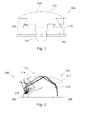
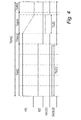
- Figures 1 and 2 show a particular type of optical navigation device module suitable for the application of the present invention.
- This optical navigation device module is described in detail in co-pending application number GB0908899.8 . It should be noted that this optical navigation device is described by way of example only, and any suitable optical navigation device using reflection off a mousing surface can be used.
- the optical navigation device module 100 includes a base plate 102, an optical element 106 which incorporates a clip 104 (the optical element will be described in greater detail below), an illumination source 108, such as an LED, and a sensor 110.
- the overall construction of the optical navigation device module 100 is of a low profile construction making it suitable for mobile devices.
- the actual size of the overall package containing the optical navigation device sits under a cap of about 7mm in diameter and the module itself has a maximum dimension of about 5.8 mm.
- the optical element 106 may be molded from a single piece of plastic and provides a so called mousing surface 112.
- An example of the type of plastic material is a monolithic optical block made of a plastics material such as poly (methyl methacrylate) also known as PMMA; although it will be appreciated other materials (such as Polycarbonate, Cyclcyclophane copolymer) may alternatively be used.
- this particular type of optical navigation device uses the optical layout for a frustrated total internal reflection (F-TIR) device 200, although direct imaging systems and other systems are equally applicable to be used in place of the F-TIR device 200.
- F-TIR frustrated total internal reflection
- the F-TIR device 200 includes an LED 202 which emits a source of radiation directed by optical element 204 to the internal surface 210 of the mousing surface 112. A further optical element 208 then directs any reflected radiation from surface 210 on to sensor 206.
- the LED 202 may be of any appropriate type and may be mounted on a substrate.
- the LED emits in the near infrared range for example between about 700 to 900 nm.
- the optical element 204 directs the LED illumination into the monolithic optical block which forms the optical element 106.
- the optical element 204 may be in any appropriate to form for example a single convex surface; a series of lenslets configured as a "fly eye” structure; or any other suitable structure capable of providing near collimated illumination at the internal surface 210.
- the optical element 204 may be capable of being tilted in order to control the illumination pattern and direction of the beam at the mousing surface.
- the mousing surface 112 includes an internal surface 210 and an external surface 212. At the mousing surface any object with a refractive index which is placed in contact with the external surface 212 will frustrate the total internal reflection of the beams 214 at the internal surface 210.
- a suitable object may include a finger, pointer, hand or other object or feature. A so-called frustrated reflection will thus be generated and the resulting pattern is focused by optical element 208 onto the sensor 206.
- the internal surface 210 is relatively smooth when compared to the features which give rise to the F-TIR. Illumination reflected from the internal surface 210 when there is no object close to the mousing surface is virtually 100% reflected. However, when the reflection is frustrated only about 10% or less of the illumination is reflected, thus resulting in contrast ratio of about 1:10 in the present example. Note that at 850 nm most of returned signal is from scattering at the object in contact with the optical element 106 (e.g. the skin of the user's finger).
- the frustrated reflection directed on to the sensor is detected in order to identify the point or points of contact of the object in contact with the external surface 212. Subsequent measurements of the point or points of contact will provide information corresponding to the movement of object on the external surface 212. The action or movement of the object can then be translated into actions to operate a mobile personal computer.
- the optical navigation device may have a backlight provided by an LED separate to the LED 202, which provides the radiation source for the sensor 206.
- a backlight provided by an LED separate to the LED 202, which provides the radiation source for the sensor 206.
- performance degradation can result. This is because the backlight illuminates the mousing surface and degrades the contrast of a fingerprint, thereby reducing the signal-noise ratio of the acquired image.
- the illumination optics ideally produces a collimated beam of light at an oblique angle (i.e. as close as possible to the plane of the surface) as possible.
- the backlighting optics produces a smooth distribution of light over the surface and is as homogenous as possible. Hence the photons from the backlighting system do not provide good contrast of surface texture.
- the backlight naturally uses wavelengths in the visible band while it is common for the navigation LED to be infra-red (IR).
- IR infra-red
- the longer wavelength IR photons penetrate the silicon deeper before generating electron-hole pairs.
- a significant portion of the photo generated charge from the IR / navigation source will be generated in the bulk of the substrate which is usually highly doped. As a result the electron-hole pairs will recombine quickly and not be collected, and the device will have a reduced quantum efficiency.
- the detector will receive a greater amount of (unwanted) signal from the visible (backlit) LED compared to the signal from the IR (navigation) LED and the image contrast will be further degraded.
- Figure 3 shows a typical timing diagram of prior art sensor operation. It shows a sensor operating in repeated cycles of four phases, during which the levels of the sensor photodiode voltage VPD, the reset line RST, the navigation LED NAVLED and the Backlight LED, BACKLED are shown.
- the four phases are: a reset phase where the sensor's pixels are all reset to a predetermined voltage level, a black calibration phase whereby the sensor is calibrated so as to determine the appropriate output level in the absence of light, an expose phase where the sensor obtains an image and a readout phase, where the obtained image is read out for comparison to previous images to determine motion.
- This basic cycle of phases is well known for any imaging sensor.
- the timing arrangement of Figure 3 attempts to solve the above signal degradation problem by turning the backlighting LED off during part of the frame so it does not interfere with the navigation operation. While it is possible to turn the backlighting LED on during dark calibration, this is disadvantageous as it would produce an offset into the pixel and reduce the dynamic range. Turning the backlight LED on during either exposure (Texpose) or readout (Treadout) will cause the degradation problems described above. Hence only if the backlight is turned on during the reset phase (Treset1) will the backlighting not degrade the imaging / navigation system.
- this reset period (Treset1) is a short period (10 ⁇ s) compared to the total frame period (100 ⁇ s). Consequently, if this period is used to provide backlighting, the resulting duty cycle of the backlight is low (10% typical). This would produce a dim back light unless the peak current through the backlighting LED was increased accordingly. It is common for LEDs to be operated in this mode and their maximum current is typically dependent on the duty cycle of operation (thermal dissipation limits, so 1A at duty cycle of 10% equals 100mA constant).
- a mouse/navigation device sensor operation is different to that of a still camera / video camera / webcam in that the mouse/navigation device sensor can control the lighting.
- a significant further difference is that of frame-rate.
- the mouse sensor operates at 1kHz-10kHz frame rate compared to 10-50Hz of a DSC/webcam.
- Figure 3 shows equal time for the black calibration phase Tblackcal and readout phase Treadout, however black calibration phase Tblackcal is typically shorter than readout phase Treadout, using the technique described in US7502061 (hereby incorporated by reference).
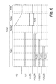
- FIG 4 is a timing diagram illustrating the operation of a navigation device with backlighting system according to an embodiment of the invention.
- the lines shown and phases (other than duration) are the same as that illustrated in Figure 3 .
- the reset phase (Treset2) has now been lengthened and is now the longest phase in the system. It is preferable that the period for which the backlight LED is on, TbLED2 is shorter than the reset phase Treset2, so that (a) the navigation device photo sensor does not detect any photons from the backlighting system, and (b) the backlighting LED is turned off in advance of the reset pulse so that the disturbance on the supply rails caused by turning off the current through the LED has disappeared before the pixel comes out of reset.
- the width of the backlight LED (TbLED2) pulse can be varied to change the average intensity of the backlighting.
- the reset (Treset2) pulse stays the same length and does not vary as the backlight LED (TbLED2) pulse varies. This keeps the frame length (Tframe2) constant which simplifies the calculation of speed of the mouse.
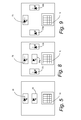
- Figure 5 shows an optical navigation device according to said first embodiment of the invention. It comprises optical sensor 10, a navigation Light Emitting Diode (LED) 20 and a white or tricolour backlighting LED 30.
- LED Navigation Light Emitting Diode
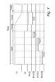
- Figure 6 illustrates such an arrangement where there are 3 separate illumination LED outputs, BACKLEDR, BACKLEDG, and BACKLEDB, each with different pulse widths.
- FIG 7 illustrates an alternative arrangement to that illustrated in Figure 6 .
- the pulses for the backlighting LED channels BACKLEDR, BACKLEDG, BACKLEDB are non-overlapping. They are set such that as one turns off another is turned on. Not only does this reduce the maximum current required for backlighting to 1/3 of the system shown in Figure 6 (assuming same current through each LED colour), but it keeps the current drain roughly constant during the reset period. In both cases this helps to minimise the inrush current into the mouse module.
- Figure 8 shows an optical navigation device according to said first embodiment of the invention. It comprises optical sensor 10, a navigation Light Emitting Diode (LED) 20 and three backlighting LEDs, red 30r, green 30g and blue 30b.
- LED Navigation Light Emitting Diode
- the LEDs are red, green and blue, these being additive primary colours that allow an illumination output in the other visible colours of the spectrum.
- the blue LED signal (BACKLEDB) is on for about the same period as the green LED signal (BACKLEDG) but only half the time of the red LED signal (BACKLEDR), i.e. duration of signal TbbLED4 equals duration of signal TbgLED4 equals 2 x duration of signal TbrLED4.
- the ratio of the periods sets the colour of the backlight.
- the total duration of signals TbbLED4, TbgLED4 and TbrLED4 is less than the duration of Treset4.
- the actual width / duty cycle of the backlighting pulse can be set in variety of manners.
- Figure 9 shows a variation on the optical navigation device according to Figure 8 .
- only two illumination LEDs are provided, a red and green bi-colour LED 30rg and a blue LED 30b.
- the navigation device has, in some embodiments, a memory (e.g. 12C or SPI register) which the host controller of the host device (for example, phone, MP3 player or similar portable media player (PMP), Digital Still camera, satellite navigation system, remote control) can access to program the brightness / colour / width of the backlighting LED pulse.
- a memory e.g. 12C or SPI register
- PMP portable media player
- Digital Still camera satellite navigation system, remote control
- the backlighting can also be controlled by the navigation device itself, as illustrated by the following examples.
- the backlighting can be inhibited to reduce energy consumption (as the user's finger is probably obscuring the surface, it is not sensible to use energy to illuminate the user's finger as the lighting cannot be observed).
- navigation device engine It is common for navigation device engine to detect the presence or absence of features on the surface. This signal can also be used to control (e.g. enable / disable) the backlighting.
- the host would request that the RED LED was turned on (for example to indicate a. low battery warning), but only at the appropriate time, that is in the absence of motion over the surface of the sensor (i.e. finger not moving on the surface).
- This gating can be easily controlled by setting / clearing appropriate control bits via 12C or SPI register command.
- the host could then program in a particular colour, e.g. pink N ⁇ 0xFF # Red value N+1 ⁇ 0xC0 # Green value N+2 ⁇ 0xCB # Blue value
- the device would automatically adjust the periods of TbrLED4 TbgLED4 & TbbLED4 to maintain the correct ratio. Further, if the host wished to dim the backlight and keep the same colour, only a single register write is required.
- the navigation device sensor integrate an ambient light detector (for an example, see applicant's co-pending application- attorney ref P113944.GB.01) not only should the navigation LED be disabled when device is measuring ambient light, but also the background illumination should be disabled when the device is measuring ambient light.
- the sensor for detecting ambient light may, in an embodiment, be the same sensor as the navigation device sensor.
- optical navigation device is not relevant so long as it is of a type that uses a radiation device and sensor to determine movement and at least a further radiation device for illumination.
- the above non-exhaustive list of possible examples are purely illustrative of the utility of the invention disclosed herein.
Landscapes
- Engineering & Computer Science (AREA)
- Physics & Mathematics (AREA)
- General Engineering & Computer Science (AREA)
- Theoretical Computer Science (AREA)
- General Physics & Mathematics (AREA)
- Human Computer Interaction (AREA)
- Electromagnetism (AREA)
- Radar, Positioning & Navigation (AREA)
- Remote Sensing (AREA)
- Position Input By Displaying (AREA)
Applications Claiming Priority (1)
| Application Number | Priority Date | Filing Date | Title |
|---|---|---|---|
| GBGB0921644.1A GB0921644D0 (en) | 2009-12-10 | 2009-12-10 | Improvements in or relating to optical navigation devices |
Publications (1)
| Publication Number | Publication Date |
|---|---|
| EP2336860A1 true EP2336860A1 (de) | 2011-06-22 |
Family
ID=41666907
Family Applications (1)
| Application Number | Title | Priority Date | Filing Date |
|---|---|---|---|
| EP10194281A Withdrawn EP2336860A1 (de) | 2009-12-10 | 2010-12-09 | Verbesserungen an - oder im Zusammenhang mit - optischen Navigationsgeräten |
Country Status (3)
| Country | Link |
|---|---|
| US (1) | US9354747B2 (de) |
| EP (1) | EP2336860A1 (de) |
| GB (1) | GB0921644D0 (de) |
Families Citing this family (4)
| Publication number | Priority date | Publication date | Assignee | Title |
|---|---|---|---|---|
| GB2497572A (en) * | 2011-12-15 | 2013-06-19 | St Microelectronics Ltd | Function performance in response to pattern recognition on an optical navigation device such as a finger mouse |
| US9927915B2 (en) | 2014-09-26 | 2018-03-27 | Cypress Semiconductor Corporation | Optical navigation systems and methods for background light detection and avoiding false detection and auto-movement |
| WO2021147020A1 (zh) * | 2020-01-22 | 2021-07-29 | 深圳市汇顶科技股份有限公司 | 指纹识别装置和电子设备 |
| US20210247516A1 (en) * | 2020-02-11 | 2021-08-12 | Visual Sensing Technology Co., Ltd. | Optical navigation apparatus |
Citations (6)
| Publication number | Priority date | Publication date | Assignee | Title |
|---|---|---|---|---|
| US6969879B2 (en) | 2002-08-22 | 2005-11-29 | Stmicroelectronics Ltd. | Solid state image sensor |
| US20080252618A1 (en) * | 2006-09-26 | 2008-10-16 | In Jae Chung | Display having infrared edge illumination and multi-touch sensing function |
| US20090027358A1 (en) * | 2007-07-26 | 2009-01-29 | Kabushiki Kaisha Toshiba | Input display apparatus and input display panel |
| US7502061B2 (en) | 2003-11-04 | 2009-03-10 | Stmicroelectronics Ltd. | Method for image sensor calibration and associated devices |
| US20090161051A1 (en) * | 2007-12-19 | 2009-06-25 | Sony Corporation | Display device |
| US20090289920A1 (en) * | 2008-05-22 | 2009-11-26 | Au Optronics Corporation | Optical reflected touch panel and pixels and system thereof |
Family Cites Families (19)
| Publication number | Priority date | Publication date | Assignee | Title |
|---|---|---|---|---|
| US4837631A (en) * | 1987-09-14 | 1989-06-06 | Peter D. Sahagen | Electronic still camera tube |
| US6452633B1 (en) * | 1998-02-26 | 2002-09-17 | Foveon, Inc. | Exposure control in electronic cameras by detecting overflow from active pixels |
| US20040252867A1 (en) * | 2000-01-05 | 2004-12-16 | Je-Hsiung Lan | Biometric sensor |
| US7361860B2 (en) | 2001-11-20 | 2008-04-22 | Touchsensor Technologies, Llc | Integrated touch sensor and light apparatus |
| US6906304B2 (en) * | 2002-11-27 | 2005-06-14 | Microsoft Corporation | Photo-sensor array for motion detection |
| US7593593B2 (en) | 2004-06-16 | 2009-09-22 | Microsoft Corporation | Method and system for reducing effects of undesired signals in an infrared imaging system |
| JP2006018566A (ja) | 2004-07-01 | 2006-01-19 | Canon Inc | 光学式座標入力装置 |
| JP4072732B2 (ja) | 2004-10-29 | 2008-04-09 | ソニー株式会社 | 入出力装置および方法、記録媒体、並びにプログラム |
| US7488926B2 (en) * | 2006-01-06 | 2009-02-10 | Microsoft Corporation | Pixel array with shared pixel output lines |
| US20070164999A1 (en) * | 2006-01-19 | 2007-07-19 | Gruhlke Russell W | Optical navigation module and lens having large depth of field therefore |
| US7557338B2 (en) * | 2006-03-14 | 2009-07-07 | Avago Technologies General Ip (Singapore) Pte. Ltd. | Electronic device with integrated optical navigation module and microlens array therefore |
| JP4162023B2 (ja) * | 2006-08-24 | 2008-10-08 | ミツミ電機株式会社 | 指紋検出装置 |
| US7924272B2 (en) * | 2006-11-27 | 2011-04-12 | Microsoft Corporation | Infrared sensor integrated in a touch panel |
| US8674949B2 (en) | 2007-02-20 | 2014-03-18 | Japan Displays Inc. | Liquid crystal display apparatus |
| US7486386B1 (en) * | 2007-09-21 | 2009-02-03 | Silison Laboratories Inc. | Optical reflectance proximity sensor |
| US20090213093A1 (en) | 2008-01-07 | 2009-08-27 | Next Holdings Limited | Optical position sensor using retroreflection |
| JP4915367B2 (ja) | 2008-02-27 | 2012-04-11 | ソニー株式会社 | 表示撮像装置および物体の検出方法 |
| US8736587B2 (en) * | 2008-07-10 | 2014-05-27 | Semiconductor Energy Laboratory Co., Ltd. | Semiconductor device |
| GB2470553A (en) | 2009-05-26 | 2010-12-01 | St Microelectronics Ltd | Optical computer input with single frustrated total internal reflection mousing surface |
-
2009
- 2009-12-10 GB GBGB0921644.1A patent/GB0921644D0/en not_active Ceased
-
2010
- 2010-12-09 EP EP10194281A patent/EP2336860A1/de not_active Withdrawn
- 2010-12-09 US US12/964,146 patent/US9354747B2/en not_active Expired - Fee Related
Patent Citations (6)
| Publication number | Priority date | Publication date | Assignee | Title |
|---|---|---|---|---|
| US6969879B2 (en) | 2002-08-22 | 2005-11-29 | Stmicroelectronics Ltd. | Solid state image sensor |
| US7502061B2 (en) | 2003-11-04 | 2009-03-10 | Stmicroelectronics Ltd. | Method for image sensor calibration and associated devices |
| US20080252618A1 (en) * | 2006-09-26 | 2008-10-16 | In Jae Chung | Display having infrared edge illumination and multi-touch sensing function |
| US20090027358A1 (en) * | 2007-07-26 | 2009-01-29 | Kabushiki Kaisha Toshiba | Input display apparatus and input display panel |
| US20090161051A1 (en) * | 2007-12-19 | 2009-06-25 | Sony Corporation | Display device |
| US20090289920A1 (en) * | 2008-05-22 | 2009-11-26 | Au Optronics Corporation | Optical reflected touch panel and pixels and system thereof |
Non-Patent Citations (1)
| Title |
|---|
| HAN J Y: "Low-cost multi-touch sensing through frustrated total internal reflection", UIST 05. PROCEEDINGS OF THE 18TH. ANNUAL ACM SYMPOSIUM ON USER INTERFACE SOFTWARE AND TECHNOLOGY,, 23 October 2005 (2005-10-23), pages 115 - 118, XP007905448, ISBN: 978-1-59593-023-1, Retrieved from the Internet <URL:http://portal.acm.org/citation.cfm?id=1095054> * |
Also Published As
| Publication number | Publication date |
|---|---|
| GB0921644D0 (en) | 2010-01-27 |
| US20110141487A1 (en) | 2011-06-16 |
| US9354747B2 (en) | 2016-05-31 |
Similar Documents
| Publication | Publication Date | Title |
|---|---|---|
| US11030946B1 (en) | Ambient brightness detection method, electronic device, detection apparatus and storage medium | |
| US8638317B2 (en) | Display apparatus and method for controlling the same | |
| US8681255B2 (en) | Integrated low power depth camera and projection device | |
| US8212794B2 (en) | Optical finger navigation utilizing quantized movement information | |
| US9622326B1 (en) | Method and device for determining emitted light intensity level | |
| JP4884552B2 (ja) | 照度、近接度及び色温度の測定が可能なイメージセンサ | |
| US8304727B2 (en) | Image sensor capable of judging proximity to subject | |
| US20100127159A1 (en) | Photodetecting semiconductor apparatus and mobile device | |
| US20070296688A1 (en) | Liquid crystal display device achieving imaging with high s/n ratio using invisible light | |
| CN113077738A (zh) | 环境光检测方法及装置、存储介质 | |
| CN107426471A (zh) | 相机模组和电子装置 | |
| Ma et al. | Automatic brightness control of the handheld device display with low illumination | |
| EP2336860A1 (de) | Verbesserungen an - oder im Zusammenhang mit - optischen Navigationsgeräten | |
| WO2005072193A2 (en) | Graphical code reader having illumination leds of different wavelengths | |
| WO2017041409A1 (zh) | 一种电子产品及其logo显示方法、系统 | |
| JPH10222285A (ja) | 画像抽出装置 | |
| KR20120095681A (ko) | 이미지 센서 및 이를 포함하는 촬영 장치 | |
| US8358282B2 (en) | Object detection device | |
| CN205793075U (zh) | 显示模块和电子设备 | |
| US20250016465A1 (en) | Monolithic Image Sensor, a Camera Module, an Electronic Device and a Method for Operating a Camera Module | |
| US20110025604A1 (en) | System for adjusting a light output of an optical mouse and a mouse thereof | |
| US8400413B2 (en) | Display apparatus and display method | |
| US20060033015A1 (en) | Optical mouse with reduced power consumption | |
| JP2010256066A (ja) | 光学センサおよびそれを備えた機器 | |
| US20250097588A1 (en) | Brightness detection method and apparatus, control method and apparatus for photographic apparatus, and medium |
Legal Events
| Date | Code | Title | Description |
|---|---|---|---|
| PUAI | Public reference made under article 153(3) epc to a published international application that has entered the european phase |
Free format text: ORIGINAL CODE: 0009012 |
|
| AK | Designated contracting states |
Kind code of ref document: A1 Designated state(s): AL AT BE BG CH CY CZ DE DK EE ES FI FR GB GR HR HU IE IS IT LI LT LU LV MC MK MT NL NO PL PT RO RS SE SI SK SM TR |
|
| AX | Request for extension of the european patent |
Extension state: BA ME |
|
| 17P | Request for examination filed |
Effective date: 20111221 |
|
| STAA | Information on the status of an ep patent application or granted ep patent |
Free format text: STATUS: THE APPLICATION IS DEEMED TO BE WITHDRAWN |
|
| 18D | Application deemed to be withdrawn |
Effective date: 20150701 |