EP2337263B1 - Token mit verbesserter unklonbarer physikalischer Funktion - Google Patents
Token mit verbesserter unklonbarer physikalischer Funktion Download PDFInfo
- Publication number
- EP2337263B1 EP2337263B1 EP09179628.4A EP09179628A EP2337263B1 EP 2337263 B1 EP2337263 B1 EP 2337263B1 EP 09179628 A EP09179628 A EP 09179628A EP 2337263 B1 EP2337263 B1 EP 2337263B1
- Authority
- EP
- European Patent Office
- Prior art keywords
- conducting particles
- dielectric medium
- heating
- structural state
- token
- Prior art date
- Legal status (The legal status is an assumption and is not a legal conclusion. Google has not performed a legal analysis and makes no representation as to the accuracy of the status listed.)
- Active
Links
Images




Classifications
-
- H—ELECTRICITY
- H04—ELECTRIC COMMUNICATION TECHNIQUE
- H04L—TRANSMISSION OF DIGITAL INFORMATION, e.g. TELEGRAPHIC COMMUNICATION
- H04L9/00—Cryptographic mechanisms or cryptographic arrangements for secret or secure communications; Network security protocols
- H04L9/32—Cryptographic mechanisms or cryptographic arrangements for secret or secure communications; Network security protocols including means for verifying the identity or authority of a user of the system or for message authentication, e.g. authorization, entity authentication, data integrity or data verification, non-repudiation, key authentication or verification of credentials
- H04L9/3271—Cryptographic mechanisms or cryptographic arrangements for secret or secure communications; Network security protocols including means for verifying the identity or authority of a user of the system or for message authentication, e.g. authorization, entity authentication, data integrity or data verification, non-repudiation, key authentication or verification of credentials using challenge-response
- H04L9/3278—Cryptographic mechanisms or cryptographic arrangements for secret or secure communications; Network security protocols including means for verifying the identity or authority of a user of the system or for message authentication, e.g. authorization, entity authentication, data integrity or data verification, non-repudiation, key authentication or verification of credentials using challenge-response using physically unclonable functions [PUF]
-
- G—PHYSICS
- G06—COMPUTING OR CALCULATING; COUNTING
- G06F—ELECTRIC DIGITAL DATA PROCESSING
- G06F21/00—Security arrangements for protecting computers, components thereof, programs or data against unauthorised activity
- G06F21/70—Protecting specific internal or peripheral components, in which the protection of a component leads to protection of the entire computer
- G06F21/71—Protecting specific internal or peripheral components, in which the protection of a component leads to protection of the entire computer to assure secure computing or processing of information
- G06F21/73—Protecting specific internal or peripheral components, in which the protection of a component leads to protection of the entire computer to assure secure computing or processing of information by creating or determining hardware identification, e.g. serial numbers
-
- G—PHYSICS
- G09—EDUCATION; CRYPTOGRAPHY; DISPLAY; ADVERTISING; SEALS
- G09C—CIPHERING OR DECIPHERING APPARATUS FOR CRYPTOGRAPHIC OR OTHER PURPOSES INVOLVING THE NEED FOR SECRECY
- G09C1/00—Apparatus or methods whereby a given sequence of signs, e.g. an intelligible text, is transformed into an unintelligible sequence of signs by transposing the signs or groups of signs or by replacing them by others according to a predetermined system
-
- H—ELECTRICITY
- H04—ELECTRIC COMMUNICATION TECHNIQUE
- H04L—TRANSMISSION OF DIGITAL INFORMATION, e.g. TELEGRAPHIC COMMUNICATION
- H04L2209/00—Additional information or applications relating to cryptographic mechanisms or cryptographic arrangements for secret or secure communication H04L9/00
- H04L2209/08—Randomization, e.g. dummy operations or using noise
Definitions
- the invention relates to a token comprising an improved physical unclonable function.
- the invention further relates to an integrated circuit comprising the token, to a method of randomizing the token and a system for randomizing the token.
- the invention further relates to a system for randomizing the token.
- a token is a physical element which has unique properties which enable the token to be used for identification and authentication purposes, and for the generation of encryption / decryption keys.
- Such tokens are known in the art and typically comprise a physical object that comprises the unique physical element which enables a probing device to probe the unique physical element and to obtain a unique response from this unique physical element caused by the probing.
- the unique physical element is also often referred to as the physical unclonable function or physical random function or physical one-way function. This unique response from the physical unclonable function may be used by the probing device to generate a specific bit string which may indicate that the token is authentic. Alternatively, the bit string may be used, for example, to encrypt or decrypt data.
- Many different examples of physical unclonable functions are known in the art, such as three-dimensional optical media comprising scattering elements which are distributed randomly and which generate a unique scattering distribution when illuminated with, for example, a laser beam.
- Physical unclonable functions may also be constituted by a capacitor comprising a dielectric medium arranged between the electrodes of the capacitor, in which the dielectric medium comprises a distribution of conducting particles.
- Such physical unclonable functions are, for example, known from WO 2007/069190 . Because both the distribution of the conducting particles in the dielectric medium and the shape of the individual conducting particles are substantially random, the capacitance measured from the capacitor being the physical unclonable function is also substantially random.
- a benefit when using the physical unclonable function constituted by a capacitor is that it enables the physical unclonable function to be relatively easily embedded in a chip, for example, on a smart card and used, for example, in secure transactions.
- a problem with such known physical unclonable functions constituted by a capacitor is that a bandwidth within which the randomness of the capacitance varies is relatively limited.
- WO 2008/152577 A1 discloses a method and system for providing digital security by means of a reconfigurable physical uncloneable function (RPUF).
- the RPUF comprises a physical system constituted by distributed components arranged to generate a first response when receiving a first challenge at a point of the physical system.
- the physical reconfiguring of the RPUF comprises redistributing the components such that they generate a second response, which differs from said first response, when again applying the first challenge at the point.
- the reconfiguration step is further utilized in providing secure storage for digital items.
- the digital item is data of any kind, including data that needs to be accessed and updated, i.e. which is dynamic in nature.
- the method is exemplified by implementations such as secure storage of a key, a secure counter and a seed generator.
- the invention in a first aspect, relates a token comprising a physical unclonable function and comprising probing means for probing the physical unclonable function to obtain a unique response in response to the probing,
- the physical unclonable function comprising a capacitor comprising a dielectric medium being arranged at least partially between the electrodes of the capacitor and being configured for contributing to a capacitance value of the capacitor, the dielectric medium comprising conducting particles substantially randomly dispersed in the dielectric medium, the conducting particles comprising a phase changeable material being changeable between a first structural state having a first conductivity and a second structural state having a second conductivity different from the first conductivity.
- a token is a physical element which has unique properties which enable the token to be used for identification and authentication purposes, and for the generation of encryption / decryption keys.
- the token also often referred to as security token, hardware token, authentication token, cryptographic token, and software token typically acts as an electronic key and may, for example, be used in addition to or in place of a password to prove that a person is who he claims to be.
- the unique property may, for example, be a randomized capacitance value of a capacitor integrated in the token. By scanning the capacitor via a read-out circuit, the unique property may be captured and used for identification. Examples of tokens are, for example, a banking card, a smart card, or a device comprising a randomized physical parameter which is specific for the device, or specific for the integrated circuit on the device, or specific for the capacitor read-out circuit.
- Phase changeable material is a material which, upon a trigger, may alter its structural state, for example, from a crystalline state into an amorphous state.
- the phase changeable material is configured for altering the structural state while maintaining dispersed in the dielectric medium.
- the phase changeable material may, for example, be heated to above a threshold temperature causing the phase changeable material to melt.
- the rate of cooling after having been molten determines the resulting structural state of the phase changeable material.
- the rate of cooling may strongly vary throughout the dielectric material and typically randomly varies throughout the dielectric material which causes the changing of the phase of the phase changeable material after heating above the threshold temperature to become substantially random within the dielectric medium.
- phase changeable materials for example, comprise chalcogenide material which is also commonly used in re-writable compact discs (CD) and re-writable digital video discs (DVD).
- Chalcogenide materials comprise, for example, Ge 2 Sb 2 Te 5 and many other Ge k In l Sb m Te n combinations, in which k, l, m and n may be in a range between 0 and 100.
- the effect of the token according to the invention is that an additional element of complexity is added to the physical unclonable function constituted by a capacitor. Due to the difference in conductivity and due to the changeability of this difference in conductivity, the randomness of the capacitance of the physical unclonable function is substantially enhanced.
- the subsequent rate of cooling is strongly determined by the surroundings of the conducting particle comprising the phase changeable material.
- the location of a first conducting particle in the dielectric medium comprises a surrounding of a first conducting particle which may, for example, enhance the cooling speed of the first conducting particle resulting in the phase changeable material in this first conducting particle, after having been through the heating and cooling phases, to end up in an amorphous state which result in a relatively low conductivity.
- a second conducting particle has different surroundings such that, for example, the thermal energy may not easily flow away from this second conducting particle which results in a reduced cooling speed and consequently in a crystalline state having relatively high conductivity.
- the surroundings of the individual conducting particles is almost impossible to actively influence, it becomes substantially unpredictable which of the conducting particles comprising phase changeable materials will change from a crystalline state into an amorphous state and vice versa.
- the conductivity of this individual particle changes which alters the overall capacitance of the physical unclonable function.
- the capacitance is based only on the randomness of the distribution of the conducting particles dispersed in the dielectric medium between the electrodes of the capacitor.
- the distribution of the particles in the dielectric medium of the known physical unclonable functions is fixed, and because the distribution of the particles in the dielectric medium relates to the capacitance distribution of other three dimensional capacitors on the chip, a smart hacker may find out the capacitance distribution of the chip and may hack the stored data in it.
- the distribution of the conducting particles is substantially random, comparable with the known physical unclonable functions, but on top of that the conductive properties of the individual conducting particles may be altered and this altering of the conductive properties of the individual conducting particles may be performed substantially randomly.
- the structural state to which the phase changeable material returns is depending strongly on the local surroundings of the individual conducting particles which makes the changing of the phase changeable material substantially unpredictable substantially increasing the randomness of the physical unclonable function and enhancing the security of the physical unclonable function.
- the different phase typically also has different conductive properties, the range over which the capacitance of the capacitor constituting the physical unclonable function varies increases.
- the difference between the first conductivity and the second conductivity is at least one order of magnitude, and/or at least two orders of magnitude, and/or at least three orders of magnitude.
- This change of at least two orders of magnitude enable the dimensions of the capacitor constituting the physical unclonable function to be reduced while still obtaining a significant change in dielectric constant of the capacitor.
- This change of at least three orders of magnitude increase the randomness and bandwidth of the capacitor while enabling the dimensions of the capacitor to remain limited.
- the difference between the first conductivity and second conductivity may result in an overall change of the dielectric constant and as such determines the range within which the capacitance value of the capacitor may vary and consequently determines the range and bandwidth in the randomness which may be expected in the capacitance value of the capacitor.
- a relatively large bandwidth of randomly defined capacitance values of the capacitor generates a larger range in randomness of the capacitance value in the token and consequently a more secure token.
- the phase changeable material in the first structural state comprises a conductive material and in the second structural state comprises a dielectric material.
- Phase changeable materials which change from a conductive material into a dielectric material and vice versa have an even higher difference between the first conductivity and the second conductivity than the previously mentioned three orders of magnitude because the dielectric material substantially behaves as an insulator.
- Such materials are, for example, known as chalcogenide materials used in re-writable compact discs and DVDs. This huge difference in conductivity of the phase changeable material in the first structural state and the second structural state enable a significant increase in randomness and bandwidth of the physical unclonable function, while the capacitor may still be integrated in an integrated circuit.
- a further effect of the embodiment in which the second structural state comprises a dielectric material is that the dielectric permittivity of the capacitor changes. If the phase changeable material transforms into a non-conducting state (such as the dielectric material) the phase changeable material will behave like an isolator strongly influencing the dielectric permittivity of the capacitor.
- the first structural state is a crystalline state of the phase changeable material
- the second structural state is an amorphous state of the phase changeable material.
- phase changeable material may, for example, be chalcogenide material which is also commonly used in re-writable compact discs (CD) and re-writable digital video discs (DVD).
- Chalcogens are the chemical elements in group 16 of the periodic table.
- the term chalcogenide is more commonly reserved for sulfides, selenides, and tellurides, for example, Ge 2 Sb 2 Te 5 and many other Ge k In l Sb m Te n combinations, in which k, l, m and n may be in a range between 0 and 100.
- Phase changeable material may, for example, also and alternatively comprise Se. Also materials like AgInSbTe may be suitable as phase changeable material. Also other less common materials such as InSe, SbSe, SbTe, InSbSe, InSbTe, GeSbSe, GeSbTeSe, and AgInSbSeTe may be used.
- the dielectric medium surrounding the conducting particles is configured for allowing the phase changeable material to also change a shape of the phase changeable material when changing from the first structural state to the second structural state and/or vice versa.
- the dielectric medium may, for example, comprise Al 2 O 3 , TiO 2 , SiO 2 , ZrO 2 , HfO 2 particles which will cause the whole dielectric medium to expand and contract during heating and cooling cycle, depending on thermal expansion coefficient of the different materials present in the dielectric medium. This determines the final state which is "freezed-in" when the dielectric medium is cooled. During the heating and cooling some rearrangement of the particles and/or coalescence could take place changing the overall dielectric properties. Moreover, in the matrix there will be always some space/grain boundaries that allow reshaping/restructuring of the phase change materials.
- the conductivity of the phase changeable material changes but also - if possible - the shape of the particle constituted by the phase changeable material.
- the electric field which propagates between the electrodes of the capacitor depends very much on the shape of the individual conducting particles dispersed in the dielectric medium.
- relatively sharp corners of a conducting particle typically comprise a relatively high flux density.
- the dielectric medium which may comprise a polymer matrix which may be deformable and which may, for example, allow the conducting particles to change their shape or form between the first structural state and the second structural state.
- a protective layer covers the electrodes of the capacitor, the protective layer comprising the dielectric medium.
- a protective layer may, for example, comprise a deformable resist layer having conducting particles dispersed in the resist layer. These conducting particles comprise phase changeable material.
- the protective layer may be spin coated on the surface comprising the electrodes of the capacitor.
- a protective dielectric layer can be applied over the electrodes to avoid large electrical contact between the electrodes if, for example, the metallic /phase change loading is relatively large.
- At least a part of the conducting particles and/or at least a part of the dielectric medium further comprise absorption material configured for absorbing a predefined range of electromagnetic radiation for heating the conducting particles.
- the absorption material may enhance the heating of the conducting particles and/or of the dielectric medium to more easily heat the conducting particles comprising the phase changing material to a temperature above the threshold temperature causing the phase changeable material in the conducting particles to melt and subsequently, while cooling down, resulting in one of the first or second structural state.
- the absorption material may be present, for example, in all conducting particles to enhance the local heating of the conducting particles while ensuring that the dielectric medium is not heated too much.
- the absorption material may only be present in part of the conducting particles which may, for example, be mixed with conducting particles not having the absorption material. This mixture of the two different conducting particles further enhances the randomness in the physical unclonable function of the token. Even further alternatively, the absorption material may be present in the dielectric medium. Furthermore, by adapting and/or controlling the power and/or duration of the irradiation of the capacitor based physical unclonable function with the electromagnetic radiation, a further variation and uncertainty is added to the capacitance of the capacitor based physical unclonable function further improving the randomness of the physical unclonable function and consequently the security of the token.
- At least a part of the conducting particles and/or at least a part of the dielectric medium further comprise heat extraction material configured for enhancing the extraction of heat away from the conducting particles.
- the presence of heat extraction material may locally change the cooling rate of individual conducting particles in the dielectric medium which greatly alters the final state of the phase change material.
- the conducting particles comprise a size distribution for absorbing a predefined range of electromagnetic radiation for heating the conducting particles.
- a particle size distribution of the conducting particles comprising the phase change material causes a variation in the absorption of the electromagnetic radiation.
- the heating and cooling rates will be different under illumination, physical heating and high current conditions.
- small particles tend to coalesce when molten which will increase randomness
- the token comprises altering means for altering the structural state of at least a part of the conducting particles in the dielectric medium for altering the capacitance value of the capacitor.
- altering means may comprise, for example, a heating wire arranged near the dielectric medium for at least heating a part of the dielectric medium, and consequently a part of the conducting particles dispersed in the dielectric medium.
- altering means may also comprise means for forcing a relatively high current through the capacitor which causes an electrical breakdown which may modify the structural state of the phase changeable material which changes the overall capacitance.
- This altering means may be seen as a safety regulation which may, for example, be used as a self-destruct element of the token.
- the token When the token is tampered with, for example, extensively probed to find regularities in the particle distribution in the token, the token may activate the altering means to alter the structural state of part of the phase changeable material in part of the conducting particles which results in a different capacitance value of the physical unclonable function.
- the token when probed with a probing device to verify its authenticity, will sense a different capacitance and as such will no longer accept the token as authentic.
- the physical unclonable function is part of a bank card
- the hacker may try to tamper with the capacitance to unveil its secret and its code to abuse the bank card.
- the capacitance value together with a code may be the unique combination which enables the owner to access his / her bank account.
- a code for example, a bank account number
- the token changes its capacitance which results in a change in the unique combination between the capacitance value and the bank account number, and consequently destroys the authenticity of the token which makes the bank card unusable for the hacker. Consequently, abuse of the bank card is prevented.
- the altering means comprises local heating means for locally increasing the temperature of the at least a part of the conducting particles above a threshold temperature for altering the structural state of the at least a part of the conducting particles.
- These local heating means may, for example, be positioned above or below the capacitor.
- a conductive heating line may be arranged in between the combs of a capacitor or the conductive heating line may be constituted of multiple lines to create a random change in the local heating, for example, via randomly choosing a heating line from the multiple lines.
- the altering means comprises means for applying a relatively high current through the capacitor for at least partially causing an electrical breakdown for modifying at least a part of the structural state of the phase changeable material.
- the altering means comprises local cooling means for locally adapting a cooling rate of the conducting particles for altering the structural state of the at least part of the conducting particles.
- Local cooling means may be constituted by including a Peltier element.
- local cooling means for instance, metallic or dielectric particles may be added to the dielectric medium which may function as local cooling means which actively that conduct heat. The phase changeable material which is close to these particles will experience a larger, locally enhanced cooling rate than phase changeable material which is not close to these heat conducting.
- the invention relates to an integrated circuit comprising the token according to the invention.
- the invention in a third aspect, relates to a method of randomizing a token, the token comprising a physical unclonable function comprising a capacitor comprising a dielectric medium arranged at least partially between the electrodes of the capacitor and being configured for contributing to a capacitance value of the capacitor, the dielectric medium comprising conducting particles substantially randomly dispersed in the dielectric medium, the conducting particles comprising a phase changeable material being changeable between a first structural state having a first conductivity and a second structural state having a second conductivity different from the first conductivity, the method comprising a step of altering the structural state of at least a part of the conducting particles in the dielectric medium for altering the capacitance value of the capacitor.
- the phase changeable material is configured for altering the structural state of the phase changeable material while maintaining dispersed in the dielectric medium.
- the change of the phase of a conducting particle changes the conductivity of that specific conducting particle and may also change the dielectric permittivity. Furthermore, whether a particle changes from, for example, a crystalline phase into an amorphous phase depends on the immediate surroundings of the conducting particle which is substantially random.
- the step of altering the structural state of the at least a part of the conducting particles comprises the steps of
- the step of heating the at least part of the conducting particles comprises applying a condensed beam of electromagnetic radiation to at least a part of the dielectric medium comprising the at least part of the conducting particles.
- sources for emitting the condensed beam of electromagnetic radiation are readily available and allow a relatively cost-effective way of heating the at least part of the dielectric medium.
- using, for example, lasers enable the condensed beam of electromagnetic radiation to be applied locally as the focus of the condensed beam may be made relatively small. As only part of the dielectric medium is illuminated and as it may not be apparent which part is illuminated, the use of the condensed beam of electromagnetic radiation further enhances the randomness of the capacitance value in the capacitor based physical unclonable function.
- the step of heating the at least part of the conducting particles comprises applying a varying condensed beam of electromagnetic radiation to at least a part of the dielectric medium comprising the at least part of the conducting particles. Varying the applied power or varying the time during which the condensed beam of electromagnetic radiation is applied to the dielectric medium may alter the rate of change from the first structural state to the second structural state in the dielectric medium of the capacitor based physical unclonable function, again enhancing the randomness.
- the step of heating the at least part of the conducting particles comprises applying a plurality of condensed beams of electromagnetic radiation, each of the plurality of condensed beams illuminating a corresponding part of the dielectric medium comprising the at least part of the conducting particles, the plurality of condensed beams are applied to the dielectric medium in a randomized pattern of the plurality of condensed beams.
- the plurality of condensed beams may, for example, comprise electromagnetic radiation having different wavelengths.
- part of the conducting particles may comprise absorption material absorbing a first range of electromagnetic radiation and a further part of the conducting particles may comprise a further absorption material absorbing a second range of electromagnetic radiation, different from the first range of electromagnetic radiation.
- the step of heating the at least part of the conducting particles comprises applying a heating current through a heating wire arranged near at least a part of the dielectric medium comprising the at least part of the conducting particles.
- This embodiment has as an advantage that the heating wire may be applied relatively easily.
- one or a selection of these heating wires of the plurality of heating wires may be chosen substantially randomly to enhance the randomness of the physical unclonable function.
- the step of heating the at least part of the conducting particles comprises applying a heating current through a mesh of heating wires.
- the selected heating wires in the mesh of heating wires used for applying the heating current may be selected substantially randomly.
- the step of heating the at least part of the conducting particles comprises applying a relatively high current through the capacitor for at least partially causing an electrical breakdown for modifying at least a part of the structural state of the phase changeable material.
- the applying of the relatively high electrical current changes the state of the phase changeable material which is the basic principle of the phase change memory SET and RESET cycle used in re-writable CD or DVD.
- the electrical current will flow substantially only at locations where the crystalline phase changeable material particles touch and where the remaining dielectric material in between the capacitor electrodes is so small that electrical breakdown occurs.
- the phase changeable material around the current path will get heated and a randomized change in capacitance will occur.
- the step of cooling down the at least part of the conducting particles comprises applying forced cooling means for increasing the cooling speed of the at least part of the dielectric medium comprising the at least part of the conducting particles.
- the forced cooling down may cause the heated conducting particles to be predominantly changed to, for example, the amorphous structural state.
- the direct surroundings of an individual conducting particle determines the cooling speed and consequently the structural state of the individual conducting particle after cooling, it is almost impossible to ensure that all conducting particles in which the temperature exceeded the threshold temperature will end up in the amorphous state further adding to the randomness of the change of capacitance of the capacitor.
- the step of cooling down the at least part of the conducting particles comprises applying forced cooling means in a substantially randomized pattern for enhancing the cooling of the corresponding part of the dielectric medium comprising the at least part of the conducting particles.
- Local forced cooling means may, for example, comprise a Peltier element, for example, arranged in a pattern of Peltier elements which allow local applying of forced cooling of the conducting particles.
- the dielectric medium may be in thermal contact with conducting elements connected to a heat sink for extracting thermal energy from the corresponding parts of the dielectric medium which are in contact with the conducting elements.
- the conducting elements may be arranged in a specific distribution which may be substantially random, also enhancing the randomness via the cooling of the at least part of the conducting particles.
- the invention in a fourth aspect, relates to a system for randomizing a token, the token comprising a physical unclonable function comprising a capacitor comprising a dielectric medium arranged at least partially between the electrodes of the capacitor and being configured for contributing to a capacitance value of the capacitor, the dielectric medium comprising conducting particles substantially randomly dispersed in the dielectric medium, the conducting particles comprising phase changeable material being changeable between a first structural state having a first conductivity and a second structural state having a second conductivity different from the first conductivity, the system comprising randomizing means for altering the structural state of at least a part of the conducting particles in the dielectric medium for altering the capacitance value of the capacitor.
- the randomizing means comprises heating means for heating the at least part of the conducting particles above a threshold temperature, the heating means comprising emitting means for emitting a condensed beam of electromagnetic radiation to at least a part of the dielectric medium comprising the at least part of the conducting particles
- the randomizing means comprises heating means for heating the at least part of the conducting particles above a threshold temperature, the heating means comprising emitting means for emitting a plurality of condensed beams of electromagnetic radiation, each of the plurality of condensed beams illuminating a corresponding part of the dielectric medium comprising the at least part of the conducting particles.
- the plurality of condensed beams may comprise condensed beams emitting electromagnetic radiation having a different wavelength compared to the remaining condensed beams in the plurality of condensed beams.
- the randomizing means comprises heating means for heating the at least part of the conducting particles above a threshold temperature, the heating means comprising emitting means for emitting a plurality of condensed beams of electromagnetic radiation, each of the plurality of condensed beams illuminating a corresponding part of the dielectric medium comprising the at least part of the conducting particles, the emitting means being configured for applying the plurality of condensed beams in a randomized pattern of the plurality of condensed beams.
- the plurality of condensed beams may comprise condensed beams emitting electromagnetic radiation having a different wavelength compared to the remaining condensed beams in the plurality of condensed beams.
- the randomizing means comprises heating means for heating the at least part of the conducting particles above a threshold temperature, the heating means comprising a heating wire arranged near at least a part of the dielectric medium comprising the at least part of the conducting particles.
- the heating wire may be part of the token in which the system may, for example, provide power to the heating wire to ensure that the at least part of the dielectric medium is heated.
- the randomizing means comprises heating means for heating the at least part of the conducting particles above a threshold temperature, the heating means comprising a mesh of heating wires.
- the selected heating wires in the mesh of heating wires used for applying the heating current may be selected substantially randomly.
- the randomizing means further comprises cooling means for cooling the heated part of the conducting particles to below the further threshold temperature, the cooling means comprising a Peltier element for applying forced cooling to increase the cooling speed of the at least part of the dielectric medium comprising the at least part of the conducting particles.
- the cooling may be easily electronically controlled and may even be controlled to vary substantially randomly.
- the randomizing means further comprises cooling means for cooling the heated part of the conducting particles to below the threshold temperature, the cooling means comprising a pattern of selectable Peltier elements for applying forced cooling.
- the pattern of selectable Peltier elements may be chosen substantially randomly to a substantially randomized pattern of corresponding parts of the dielectric medium to increase the cooling speed of the corresponding parts of the dielectric medium comprising the at least part of the conducting particles.
- the randomizing means further comprises cooling means for cooling the heated part of the conducting particles to below the threshold temperature, the cooling means comprising a heat sink for applying forced cooling to increase the cooling speed of the at least part of the dielectric medium comprising the at least part of the cooling particles.
- the cooling means comprising a heat sink for applying forced cooling to increase the cooling speed of the at least part of the dielectric medium comprising the at least part of the cooling particles.
- the randomizing means further comprises cooling means for cooling the heated part of the conducting particles to below the threshold temperature, the cooling means comprising a pattern of conducting elements in thermal contact with corresponding parts of the dielectric medium and with the heat-sink for extracting thermal energy from the corresponding parts of the dielectric medium for influencing the localized forced cooling.
- the invention relates to a computer program product comprising instructions for causing a processor to perform the method in accordance with the invention.
- Figs. 1A to 1D are different embodiments of a physical unclonable function 10, 12, 14, 16 according to the invention.
- the physical unclonable function 10, 12, 14, 16 comprises a capacitor 20 which comprises a dielectric medium 30, 32 which is at least partially arranged between electrodes 20A, 20C of the capacitor 20.
- the dielectric medium 30, 32 contributes to a capacitance value of the capacitor 20.
- the dielectric medium 30, 32 comprises conducting particles 40, 42; 40A, 40B, 40C which are substantially randomly dispersed in the dielectric medium 30, 32.
- the conducting particles 40, 42; 40A, 40B, 40C comprise a phase changeable material which is changeable between a first structural state 40A, 40C having a first conductivity and a second structural state 40B having a second conductivity different from the first conductivity.
- the effect of the physical unclonable function 10, 12, 14, 16 in a token 100 is that an additional element of complexity is added to the physical unclonable function 10, 12, 14, 16 constituted by the capacitor 20 which enhances the randomness of the capacitance of the physical unclonable function 10, 12, 14, 16.
- the subsequent rate of cooling is strongly determined by the surroundings of the conducting particle 40, 42; 40A, 40B, 40C comprising the phase changeable material.
- Fig. 1A a first embodiment of the physical unclonable function 10 is shown in which two conductors 20A, 20C form the electrodes 20A, 20B of a capacitor 20.
- the dielectric medium 30 surrounding the two electrodes 20A, 20B determines the capacitance value of the capacitor 20.
- the capacitor may be constituted by electrodes 20A, 20B having any possible shape, even having a specific three-dimensional shape.
- the dielectric medium 30 contributes to the capacitance value of the capacitor.
- the dielectric medium comprises conducting particles 40 comprising the phase changeable material.
- the phase changeable material comprises, for example, the first structural state which is a crystalline state of the phase changeable material, and the second structural state which is an amorphous state of the phase changeable material.
- phase changeable material may, for example, be chalcogenide material which is also commonly used in re-writable compact discs (CD) and re-writable digital video discs (DVD).
- Chalcogens are the chemical elements in group 16 of the periodic table.
- the term chalcogenide is more commonly reserved for sulfides, selenides, and tellurides, for example, Ge 2 Sb 2 Te 5 and many other Ge k ln l Sb m Te n combinations, in which k, l, m and n may be in a range between 0 and 100.
- Phase changeable material may, for example, also and alternatively comprise Se. Also materials like AgInSbTe may be suitable as phase changeable material.
- Fig. 1A the dashed arrows indicate a possible path between the electrodes 20A, 20B of the capacitor 20.
- the possible path between the electrodes 20A, 20B may be adapted which alters the capacitance value of the capacitor 20. This is illustrated in Fig. 1B in which a part of the phase changeable material in the conducting particles 40 comprises a first structural state 40A and a part of the phase changeable material in the conducting particles comprise a second structural state 40B.
- the first structural state 40A is, for example, a crystalline state 40A of the phase changeable material having a relatively high conductivity.
- the second structural state 40B is, for example, an amorphous state 40B of the phase changeable material having a relatively low conductivity.
- the rate of cooling of the individual conducting particles 40A, 40B determines in which structural state the individual conducting particles 40A, 40B are freezed-in after having been heated above the threshold temperature T th . This rate of cooling is, for example, determined by the immediate surroundings of the individual conducting particles 40A, 40B which is substantially random. As such, the change of the structural state of the individual conducting particles 40A, 40B after having been heated above the threshold temperature T th is also substantially random.
- Fig. 1C is an embodiment of the physical unclonable function 14 in which the dielectric medium 32 surrounding the conducting particles 40B, 40C is configured for allowing the phase changeable material to also change a shape of the phase changeable material when changing from the first structural state to the second structural state and/or vice versa.
- the dielectric medium 32 may, for example, comprise Al 2 O 3 , TiO 2 , SiO 2 , ZrO 2 , HfO 2 particles which will cause the dielectric medium 32 to expand and contract during heating and cooling cycle, depending on thermal expansion coefficient of the different materials present in the dielectric medium 32.
- This heating and cooling cycle not only determines the final structural state of the conducting particles 40B, 40C, but also the specific shape of the phase changeable material and as such the specific shape of the conducting particle 40C which is "freezed-in" when the dielectric medium 32 is cooled. During the heating and cooling some rearrangement of the particles 40B, 40C and/or coalescence could take place changing the overall dielectric properties. Also some of the present space/grain boundaries may allow reshaping and/or restructuring of the phase change material in the conducting particles 40B, 40C. In Fig. 1C the conducting particles 40B indicated with reference number 40B are indicated to have an amorphous structural state, which the conducting particles 40C indicated with reference number 40C are indicated to have a crystalline structural state.
- the changing of the structure and/or shape of the conducting particles 40C in the dielectric medium 32 changes the path between the two electrodes 20A, 20B which subsequently change the capacitance value of the capacitor 20.
- relatively sharp corners of a conducting particle 40C typically comprise a relatively high flux density.
- the dielectric medium may alternatively comprise a polymer matrix 32 which may be deformable and which may, for example, allow the conducting particles 40B, 40C to change their shape or form between the first structural state and the second structural state.
- Fig. 1D is an embodiment of the physical unclonable function 16 in which the dielectric medium 30 comprises absorption material 50 (not shown) and/or in which at least a part of the conducting particles comprise absorption material 50.
- the absorption material 50 may be mixed in the material constituting the conducting particles 42 and/or the absorption material 50 may be applied as a layer at the outer surface of the conducting particles 42.
- the absorption material 50 is configured for absorbing a predefined range of electromagnetic radiation for heating the conducting particles 42.
- the absorption material 50 may be used to locally enhance the heating of the conducting particles 42 and/or of the dielectric medium 30 to more easily heat the conducting particles 42 comprising the phase changing material to a temperature above the threshold temperature T th causing the phase changeable material in the conducting particles 42 to melt and subsequently, while cooling down, resulting in one of the first or second structural state.
- the embodiment of Fig. 1D comprises a first type of conducting particles 40 not comprising the absorption material 50 and comprises a second type of conducting particles 42 which do comprise the absorption material 50. By mixing the first type of conducting particles 40 and second type of conducting particles 42 the mixture of the two different conducting particles further enhances the randomness in the physical unclonable function 16 of the token.
- the dielectric medium 30 may further comprise heat extraction material (not shown) configured for enhancing the extraction of heat away from the conducting particles 40, 42.
- the presence of heat extraction material may locally change the cooling rate of individual conducting particles 40, 42 in the dielectric medium 30 which greatly alters the final state of the phase change material.
- the conducting particles 40, 42 further comprise a size distribution.
- This size distribution of the conducting particles 40, 42 also results in a predefined absorption range of electromagnetic radiation for heating the conducting particles 40, 42.
- a particle size distribution of the conducting particles 40, 42 which comprise the phase change material causes a variation in the absorption of the electromagnetic radiation of the individual conducting particles 40, 42.
- particles having, for example, a maximum dimension may not absorb sufficient heating energy to achieve the threshold temperature T th when a predefined amount of heat is applied to the dielectric medium 30. So for a specific particle size distribution the heating and cooling rates will be different depending on the particle sizes of the individual conducting particles 40, 42 and the particle sizes of the surrounding conducting particles 40, 42.
- a further effect enhancing the randomness of the size distribution is that relatively small conducting particles 40, 42 tend to coalesce when molten which will increase randomness.
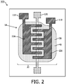
- Fig. 2 is a simplified representation of a token 100 according to the invention.
- the token 100 comprises the physical unclonable function 18 according to the invention comprising the capacitor 22 having two electrodes 22A, 22C which both have a comb-like structure arranged opposite to each other. This comb-like structure enhances the interaction surface between the two electrodes 22A, 22C which enhance the capacitance value of the capacitor 22.
- Dielectric medium 30 may be applied over the two electrodes 22A, 22C which are spaced apart. Part of the dielectric medium 30 will be positioned between the electrodes 22A, 22C to determine the capacitance value of the capacitor 22.
- the token 100 further comprises probing means 110 being contact pads which may be used by a sensing device to sense the capacitance value of the capacitor 22 constituting the physical unclonable function 18.
- the token 100 comprises altering means 120 for altering the structural state of at least a part of the conducting particles 40 in the dielectric medium 40 for altering the capacitance value of the capacitor 22.
- the altering means 120 as shown in Fig. 2 comprises a heating wire 120 arranged near the dielectric medium 30 for at least heating a part of the dielectric medium30. Consequently a part of the conducting particles 40 dispersed in the dielectric medium 30 will be heated to, for example, above the threshold temperature T th which enables the heated conducting particles 40 to alter its structural state, depending on the local cooling rate in the dielectric medium 30.
- a conductive heating line 120 may be arranged in between the combs 22A, 22C of the capacitor 22 or the conductive heating line may be constituted of multiple lines (not shown) to create a random change in the local heating, for example, via randomly choosing a heating line from the multiple lines.
- the altering means 120 may comprise means for forcing a relatively high current through the capacitor 22 (not shown) which may cause a partial electrical breakdown which may modify the structural state of the phase changeable material which changes the overall capacitance value of the capacitor 22.
- the altering means 120 may comprise local cooling means for locally adapting a cooling rate of the conducting particles for altering the structural state of the at least part of the conducting particles.
- the altering means 120 may be used as a safety regulation which may, for example, be used as a self-destruct element of the token 100.
- the token 100 may activate the altering means 120 to alter the structural state of part of the phase changeable material in part of the conducting particles 40 which results in a different capacitance value of the physical unclonable function 18.
- the token 100 when probed with a probing device to verify its authenticity, will sense a different capacitance and as such will no longer accept the token 100 as authentic.
- the physical unclonable function 100 is part of a bank card 300 (see Fig.
- a hacker may try to tamper with the capacitance 22 to unveil its secret and its code to abuse the bank card 300.
- the capacitance value together with a code for example, a bank account number may be the unique combination which enables the owner to access his / her bank account.
- the token 100 activates the altering means 120, the token 100 changes its capacitance value of the physical unclonable function 18 which results in a change in the unique combination between the capacitance value and the bank account number, and consequently destroys the authenticity of the token 100 which makes the bank card 300 unusable for the hacker. Consequently, abuse of the bank card 300 may be prevented.
- Fig. 3 is a plan-view of a smart card 300 or banking card 300 comprising an integrated circuit 200 which comprises the token 100 according to the invention.
- Figs. 4A and 4B are cross-sectional views of different embodiments of a system 500, 502 for randomizing a token 100 according to the invention.
- the system 500, 502 for randomizing the token 100 comprises randomizing means 520, 525, 530, 535, 540 for altering the structural state of at least a part of the conducting particles 40, 42; 40A, 40B, 40C (see Figs. 1A to 1D ) in the dielectric medium 30, 32 for altering the capacitance value of the capacitor 20, 22.
- the randomizing means 520, 525, 530, 535, 540 may comprise heating means 520, 525, 540 for (possibly selectively via absorption material 50 - see Fig.
- the system 500, 502 may further comprise a controller 550 for controlling the randomization of the token 100.
- the controller 550 may drive the heating means 520, 523, 540 and/or the cooling means 530, 535.
- the heating means 540 comprises means 540 for emitting a condensed beam 510, 511, 512 of electromagnetic radiation to at least a part of the dielectric medium 30, 32 comprising the at least part of the conducting particles 40, 42; 40A, 40B, 40C.
- the heating means 540 may comprise a Laser or a laser-diode or may comprise another light source which generates a condensed beam of electromagnetic radiation. In the embodiment of Fig.
- the Laser 540 emits a plurality of condensed beams 510, 511, 512 of electromagnetic radiation, each of the plurality of condensed beams 510, 511, 512 illuminating a different part of the dielectric medium 30, 32 comprising the at least part of the conducting particles 40, 42; 40A, 40B, 40C.
- the plurality of condensed beams 510, 511, 512 may comprise condensed beams emitting electromagnetic radiation having a different wavelength compared to the remaining condensed beams 510, 511, 512 in the plurality of condensed beams.
- the plurality of condensed beams 510, 511, 512 may be applied in a randomized pattern of the plurality of condensed beams 510, 511, 512 further enhancing the randomness of the physical unclonable function 10, 12, 14, 16, 18 in the token 100.
- the cooling means 530 as shown in Fig. 4A comprise a heat sink 530 for applying forced cooling to increase the cooling speed of the at least part of the dielectric medium 30, 32 comprising the at least part of the conducting particles 40, 42; 40A, 40B, 40C.
- An additional flow of cooling fluid (not shown) may be applied to further enhance the forced cooling of the heat sink 530.
- This additional flow of cooling fluid may be generated via a fan (not shown) which is controlled by the controller 550.
- a distribution of heat conducting particles in the dielectric medium 30, 32 the forced cooling of the at least part of the conducting particles 40, 42; 40A, 40B, 40C may be further enhance. Applying such heat conducting particles in a substantially random distribution further enhances the randomness of the token 100.
- the heat sink 530 may further comprise a pattern of conducting elements (not shown) which form a thermal conductive path between corresponding parts of the dielectric medium 30, 32 and the heat-sink 530 for extracting thermal energy mainly from the corresponding parts of the dielectric medium 30, 32 for influencing the localized forced cooling.
- the heating means comprising a heating wire 520 arranged near at least a part of the dielectric medium 30, 32 comprising the at least part of the conducting particles 40, 42; 40A, 40B, 40C.
- the heating wire 120, 520 may be part of the token 100 (as shown in Fig. 2 ) in which the system 500 may, for example, be configured for contacting the heating wire 120, 520 via the contact pads 110 (see Fig. 2 ) to provide power to the heating wire 120, 520 to ensure that the at least part of the dielectric medium 30, 32 is heated.
- the randomizing means 540 may comprise heating means 520, 525 by providing a mesh 525 of heating wires 520. In such an embodiment, the selected heating wires 520 in the mesh 525 of heating wires 520 used for applying the heating current may be selected substantially randomly.
- the cooling means 535 as shown in Fig. 4B further comprises cooling means comprising a Peltier element 535 for applying forced cooling to increase the cooling speed of the at least part of the dielectric medium 30, 32 comprising the at least part of the conducting particles 40, 42; 40A, 40B, 40C.
- the benefit when using a Peltier element is that the cooling may be easily electronically controlled by a controller 550 and may even be controlled to vary substantially randomly.
- the cooling means 535 may comprise a pattern of selectable Peltier elements (not individually shown) for applying forced cooling.
- the pattern of selectable Peltier elements 535 may be chosen substantially randomly to a substantially randomized pattern of corresponding parts of the dielectric medium 30, 32 to increase the cooling speed of the corresponding parts of the dielectric medium 30, 32 comprising the at least part of the conducting particles 40, 42; 40A, 40B, 40C.
- the invention may be implemented by means of hardware comprising several distinct elements, and by means of a suitably programmed computer.
- the device claim enumerating several means several of these means may be embodied by one and the same item of hardware.
- the mere fact that certain measures are recited in mutually different dependent claims does not indicate that a combination of these measures cannot be used to advantage.
- similar or corresponding features are indicated by same reference numerals or labels.
Landscapes
- Engineering & Computer Science (AREA)
- Physics & Mathematics (AREA)
- Theoretical Computer Science (AREA)
- Computer Security & Cryptography (AREA)
- General Physics & Mathematics (AREA)
- Computer Hardware Design (AREA)
- Computer Networks & Wireless Communication (AREA)
- Signal Processing (AREA)
- Mathematical Physics (AREA)
- Software Systems (AREA)
- General Engineering & Computer Science (AREA)
- Fixed Capacitors And Capacitor Manufacturing Machines (AREA)
Claims (15)
- Ein Token (100) aufweisend eine physikalische unklonbare Funktion (10, 12, 14, 16, 18) und aufweisend ein Sondierungsmittel (110) zum Sondieren der physikalischen unklonbaren Funktion (10, 12, 14, 16, 18) zum Erhalten einer einmaligen Reaktion als Reaktion auf das Sondieren,wobei die physikalische unklonbare Funktion (10, 12, 14, 16, 18) einen Kondensator (20, 22) aufweist, welcher ein dielektrisches Medium (30, 32) aufweist, welches zumindest teilweise zwischen Elektroden (20A, 20C, 22A, 22C) des Kondensators (20, 22) angeordnet ist und welches konfiguriert ist, zu einem Kapazitätswert des Kondensators (20, 22) beizutragen,wobei das dielektrische Medium (30, 32) leitfähige Partikel (40, 42; 40A, 40B, 40C) aufweist, welche im Wesentlichen zufällig in dem dielektrischen Medium (30, 32) verteilt sind, wobei die leitfähigen Partikel (40, 42; 40A, 40B, 40C) ein Phasenwechselmaterial aufweisen, welches veränderlich ist zwischen einem ersten strukturellen Zustand (40A, 40C), welcher eine erste Leitfähigkeit hat, und einem zweiten strukturellen Zustand (40B), welcher eine zweite Leitfähigkeit hat, welche verschieden zu der ersten Leitfähigkeit ist, wobei der Kapazitätswert des Kondensators (20, 22) veränderlich ist als ein Ergebnis des Wechsels zwischen dem ersten strukturellen Zustand (40A, 40C) und dem zweiten strukturellen Zustand (40B) von zumindest einem Teil der leitfähigen Partikel (40, 42; 40A, 40B, 40C),dadurch gekennzeichnet, dasszumindest ein Teil der leitfähigen Partikel (40, 42; 40A, 40B, 40C) und/oder zumindest ein Teil des leitfähigen Mediums (30, 32) ferner ein Absorptionsmaterial (50) aufweist, welches konfiguriert ist zum Absorbieren eines vordefinierten Bereichs von elektromagnetischer Strahlung zum Erwärmen der leitfähigen Partikel (40, 42; 40A, 40B, 40C), und/oderzumindest ein Teil der leitfähigen Partikel (40, 42; 40A, 40B, 40C) und/oder zumindest ein Teil des dielektrischen Mediums (30, 32) ferner ein Wärmeauskopplungsmaterial (50) aufweist, welches konfiguriert ist zum Steigern des Auskoppelns von Wärme weg von den leitfähigen Partikeln (40, 42; 40A, 40B, 40C).
- Das Token (100) gemäß Anspruch 1, wobei die Differenz zwischen der ersten Leitfähigkeit und der zweiten Leitfähigkeit zumindest eine Zehnerpotenz, und/oder zumindest zwei Zehnerpotenzen, und/oder zumindest drei Zehnerpotenzen ist, und/oder wobei das Phasenwechselmaterial in dem ersten strukturellen Zustand (40A, 40C) ein leitfähiges Material aufweist und in dem zweiten leitfähigen Zustand (40B) ein dielektrisches Material aufweist.
- Das Token (100) gemäß Anspruch 1 oder Anspruch 2, wobei der erste strukturelle Zustand (40A, 40C) ein kristalliner Zustand (40A, 40C) des Phasenwechselmaterials (40, 42; 40A, 40B, 40C) ist und wobei der zweite strukturelle Zustand (40B) ein amorpher Zustand (40B) des Phasenwechselmaterials (40, 42; 40A, 40B, 40C) ist.
- Das Token (100) gemäß Anspruch 1, 2 oder 3, wobei das dielektrische Medium (30, 32), welches die leitfähigen Partikel (40, 42; 40A, 40B, 40C) umgibt, konfiguriert ist, zu ermöglichen, dass das Phasenwechselmaterial (40, 42) eine Form des Phasenwechselmaterials (40C) ändert, wenn es sich von dem ersten strukturellen Zustand (40C) zu dem zweiten strukturellen Zustand (40B) und/oder vice versa ändert.
- Das Token (100) gemäß Anspruch 1, 2, 3 oder 4, wobei die leitfähigen Partikel (40, 42; 40A, 40B, 40C) eine Größenverteilung zum Absorbieren eines vordefinierten Bereichs von elektromagnetischer Strahlung aufweisen zum Erwärmen der leitfähigen Partikel (40, 42; 40A, 40B, 40C).
- Das Token (100) gemäß irgendeinem der vorangehenden Ansprüche, wobei das Token (100) ein Veränderungsmittel (120) aufweist zum Verändern des strukturellen Zustands von zumindest einem Teil der leitfähigen Partikel (40, 42) in dem dielektrischen Medium (30, 32) zum Verändern des Kapazitätswerts des Kondensators (20, 22).
- Das Token (100) gemäß Anspruch 6, wobei das Veränderungsmittel (120) aufweist• ein lokales Erwärmungsmittel (120) zum lokalen Erhöhen der Temperatur von zumindest einem Teil der leitfähigen Partikel (40, 42; 40A, 40B, 40C) über eine Schwellentemperatur (Tth) zum Verändern des strukturellen Zustands von dem zumindest einen Teil der leitfähigen Partikel (40, 42; 40A, 40B, 40C), und/oder• ein Mittel zum Anlegen eines relativ hohen Stroms durch den Kondensator (20, 22) zum zumindest teilweisen Veranlassen eines elektrischen Durchschlags zum Modifizieren von zumindest einem Teil des strukturellen Zustands des Phasenwechselmaterials, und/oder• ein lokales Kühlmittel zum lokalen Anpassen einer Kühlrate der leitfähigen Partikel (40, 42; 40A, 40B, 40C) zum Verändern des strukturellen Zustands von zumindest einem Teil der leitfähigen Partikel (40, 42; 40A, 40B, 40C).
- Ein integrierter Schaltkreis (200) aufweisend das Token (100) gemäß irgendeinem der Ansprüche 1 bis 7.
- Ein Verfahren zum Randomisieren eines Tokens (100), wobei das Token (100) eine physikalische unklonbare Funktion (10, 12, 14, 16, 18) aufweist, welche Sondierungsmittel aufweist zum Sondieren der physikalischen unklonbaren Funktion zum Erhalten einer einmaligen Reaktion als Reaktion auf das Sondieren;wobei die physikalische unklonbare Funktion ferner einen Kondensator (20, 22) aufweist, welcher ein dielektrisches Medium (30, 32) aufweist, welches zumindest teilweise zwischen Elektroden (20A, 20C; 22A, 22C) des Kondensators (20, 22) angeordnet ist und welches konfiguriert ist, zu einem Kapazitätswert des Kondensators (20, 22) beizutragen,wobei das dielektrische Medium (30, 32) leitfähige Partikel (40, 42; 40A, 40B, 40C) aufweist, welche im Wesentlichen zufällig in dem dielektrischen Medium (30, 32) verteilt sind, wobei die leitfähigen Partikel (40, 42; 40A, 40B, 40C) Phasenwechselmaterialien (40, 42; 40A, 40B, 40C) aufweisen, welche veränderlich sind zwischen einem ersten strukturellen Zustand (40A, 40C), welcher eine erste Leitfähigkeit hat, und einem zweiten strukturellen Zustand (40B), welcher eine zweite Leitfähigkeit hat, welche verschieden zu der ersten Leitfähigkeit ist,wobei das Verfahren einen Schritt aufweist zumVerändern des strukturellen Zustands von zumindest einem Teil der leitfähigen Partikel (40, 42; 40A, 40B, 40C) in dem dielektrischen Medium (30, 32) zum Verändern des Kapazitätswerts des Kondensators (20, 22),dadurch gekennzeichnet, dasszumindest ein Teil der leitfähigen Partikel (40, 42; 40A, 40B, 40C) und/oder zumindest ein Teil des dielektrischen Mediums (30, 32) ferner ein Absorptionsmaterial (50) aufweist, welches konfiguriert ist zum Absorbieren eines vordefinierten Bereichs von elektromagnetischer Strahlung zum Erwärmen der leitfähigen Partikel (40, 42; 40A, 40B, 40C), und/oderzumindest ein Teil der leitfähigen Partikel (40, 42; 40A, 40B, 40C) und/oder zumindest ein Teil des dielektrischen Mediums (30, 32) ferner ein Wärmeauskopplungsmaterial (50) aufweist, welches konfiguriert ist zum Steigern des Auskoppelns von Wärme weg von den leitfähigen Partikeln (40, 42; 40A, 40B, 40C).
- Das Verfahren zum Randomisieren gemäß Anspruch 9, wobei der Schritt des Veränderns des strukturellen Zustands des zumindest einen Teils der leitfähigen Partikel (40, 42; 40A, 40B, 40C) die Schritte aufweist:• Erwärmen des zumindest einen Teils der leitfähigen Partikel (40, 42; 40A, 40B, 40C) über eine Schwellentemperatur (Tth), und• Herunterkühlen des zumindest einen Teils der leitfähigen Partikel (40, 42; 40A, 40B, 40C) bis unter eine weitere Schwellentemperatur (Tfth) zum Erzeugen des ersten strukturellen Zustands (40A, 40C) und/oder des zweiten strukturellen Zustands (40B).
- Das Verfahren zum Randomisieren gemäß Anspruch 10, wobei der Schritt des Erwärmens des zumindest einen Teils der leitfähigen Partikel (40, 42; 40A, 40B, 40C) aufweist:• Anwenden eines verdichteten Strahls (510) aus elektromagnetischer Strahlung auf zumindest einen Teil des dielektrischen Mediums (30, 32), welches den zumindest einen Teil der leitfähigen Partikel (40, 42; 40A, 40B, 40C) aufweist, und/oder• Anwenden eines variierenden verdichteten Strahls (510) aus elektromagnetischer Strahlung auf zumindest einen Teil des dielektrischen Mediums (30, 32), welches den zumindest einen Teil der dielektrischen Partikel (40, 42; 40A, 40B, 40C) aufweist, und/oder• Anwenden einer Mehrzahl von verdichteten Strahlen (510, 511, 512) aus elektromagnetischer Strahlung, wobei jeder von der Mehrzahl der verdichteten Strahlen (510, 511, 512) einen korrespondierenden Teil des dielektrischen Mediums (30, 32) illuminiert, welches den zumindest einen Teil der leitfähigen Partikel (40, 42; 40A, 40B, 40C) aufweist, und/oder• Anwenden einer Mehrzahl von verdichteten Strahlen (510, 511, 512) aus elektromagnetischer Strahlung, wobei jeder von der Mehrzahl der verdichteten Strahlen (510, 511, 512) einen korrespondierenden Teil des dielektrischen Mediums (30, 32) illuminiert, welches den zumindest einen Teil der leitfähigen Partikel (40, 42; 40A, 40B, 40C) aufweist, wobei die Mehrzahl von verdichteten Strahlen (510, 511, 512) auf das dielektrische Medium (30, 32) in einem randomisierten Muster aus der Mehrzahl von verdichteten Strahlen (510, 511, 512) angewendet wird, und/oder• Anwenden eines Heizstroms (Ih) durch einen Heizdraht (520), welcher in der Nähe von zumindest einem Teil des dielektrischen Mediums (30, 32) angeordnet ist, welches den zumindest einen Teil der leitfähigen Partikel (40, 42; 40A, 40B, 40C) aufweist, und/oder• Anwenden eines Heizstroms (Ih) durch ein Netz (525) aus Heizdrähten (520),• Anwenden eines Heizstroms (Ih) durch ein Netz (525) aus Heizdrähten (520), wobei die ausgewählten Heizdrähte (520) in dem Netz (525) aus Heizdrähten (520), welche für das Anwenden des Heizstroms verwendet werden, im Wesentlichen zufällig ausgewählt werden, und/oder• Anwenden eines relativ hohen Stroms durch den Kondensator (20, 22) zum zumindest teilweisen Veranlassen eines elektrischen Durchschlags zum Modifizieren von zumindest einem Teil des strukturellen Zustands des Phasenwechselmaterials.
- Das Verfahren zum Randomisieren gemäß Anspruch 10 oder 11, wobei der Schritt des Herunterkühlens des zumindest einen Teils der leitfähigen Partikel (40, 42; 40A, 40B, 40C) aufweist:• Anwenden eines forcierten Kühlmittels (530, 535) zum Erhöhen der Kühlgeschwindigkeit des zumindest einen Teils des dielektrischen Mediums (30, 32), welches den zumindest einen Teil der leitfähigen Partikel (40, 42; 40A, 40B, 40C) aufweist, und/oder• Anwenden eines forcierten Kühlmittels (530, 535) in einem im Wesentlichen zufälligen Muster zum Steigern des Kühlens des korrespondierenden Teils des dielektrischen Mediums (30, 32), welches den zumindest einen Teil der leitfähigen Partikel (40, 42; 40A, 40B, 40C) aufweist.
- Ein System (500, 502) zum Randomisieren eines Tokens (100), wobei das Token (100) eine physikalische unklonbare Funktion (10, 12, 14, 16, 18) aufweist, welche ein Sondierungsmittel aufweist zum Sondieren der physikalischen unklonbaren Funktion, um eine einmalige Reaktion zu erhalten als Reaktion auf das Sondieren;wobei die physikalische unklonbare Funktion ferner einen Kondensator (20, 22) aufweist, welcher ein dielektrisches Medium (30, 32) aufweist, welches zumindest teilweise zwischen Elektroden (20A, 20C; 22A, 22C) des Kondensators (20, 22) angeordnet ist und welches konfiguriert ist, zu einem Kapazitätswert des Kondensators (20, 22) beizutragen, wobei das dielektrische Medium (30, 32) leitfähige Partikel (40, 42; 40A, 40B, 40C) aufweist, welche im Wesentlichen zufällig in dem dielektrischen Medium (30, 32) verteilt sind, wobei die leitfähigen Partikel (40, 42; 40A, 40B, 40C) ein Phasenwechselmaterial (40, 42; 40A, 40B, 40C) aufweisen, welches veränderlich ist zwischen einem ersten strukturellen Zustand (40A, 40C), welcher eine erste Leitfähigkeit hat, und einem zweiten strukturellen Zustand (40B), welcher eine zweite Leitfähigkeit hat, welche verschieden zu der ersten Leitfähigkeit ist,wobei das System (500, 502) ein Randomisierungsmittel (520, 525, 530, 535, 540) aufweist zum Verändern des strukturellen Zustands des zumindest einen Teils der leitfähigen Partikel (40, 42; 40A, 40B, 40C) in dem dielektrischen Medium (30, 32) zum Verändern des Kapazitätswerts des Kondensators (20, 22),dadurch gekennzeichnet, dasszumindest ein Teil der leitfähigen Partikel (40, 42; 40A, 40B, 40C) und/oder zumindest ein Teil des dielektrischen Mediums (30, 32) ferner ein Absorptionsmaterial (50) aufweist, welches konfiguriert ist zum Absorbieren eines vordefinierten Bereichs von elektromagnetischer Strahlung zum Erwärmen der leitfähigen Partikel (40, 42; 40A, 40B, 40C), und/oderzumindest ein Teil der leitfähigen Partikel (40, 42; 40A, 40B, 40C) und/oder zumindest ein Teil des dielektrischen Mediums (30, 32) ferner ein Wärmeauskopplungsmaterial (50) aufweist, welches konfiguriert ist zum Steigern des Auskoppelns von Wärme weg von den leitfähigen Partikeln (40, 42; 40A, 40B, 40C).
- Das System (500, 502) zum Randomisieren gemäß Anspruch 13, wobei das Randomisierungsmittel (520, 525, 530, 535, 540) ein Heizmittel (520, 525, 540) aufweist zum Erwärmen des zumindest einen Teils der leitfähigen Partikel (40, 42; 40A, 40B, 40C) über eine Schwellentemperatur (Tth), wobei das Heizmittel (520, 525, 540) aufweist:• ein Emittiermittel (540) zum Emittieren eines verdichteten Strahls (510) aus elektromagnetischer Strahlung zu zumindest einem Teil des dielektrischen Mediums (30, 32), welches den zumindest einen Teil der leitfähigen Partikel (40, 42; 40A, 40B, 40C) aufweist, und/oder• ein Emittiermittel (540) zum Emittieren einer Mehrzahl von verdichteten Strahlen (510, 511, 512) aus elektromagnetischer Strahlung, wobei jeder von der Mehrzahl von verdichteten Strahlen (510, 511, 512) einen korrespondierenden Teil des dielektrischen Mediums (30, 32) illuminiert, welches den zumindest einen Teil der leitfähigen Partikel (40, 42; 40A, 40B, 40C) aufweist, und/oder• ein Emittiermittel (540) zum Emittieren einer Mehrzahl von verdichteten Strahlen (510, 511, 512) aus elektromagnetischer Strahlung, wobei jeder von der Mehrzahl von verdichteten Strahlen (510, 511, 512) einen korrespondierenden Teil des dielektrischen Mediums (30, 32) illuminiert, welches den zumindest einen Teil der leitfähigen Partikel (40, 42; 40A, 40B, 40C) aufweist, wobei das Emittiermittel (540) konfiguriert ist zum Anwenden der Mehrzahl von verdichteten Strahlen (510, 511, 512) in einem randomisierten Muster aus der Mehrzahl von verdichteten Strahlen (510, 511, 512), und/oder• einen Heizdraht (520), welcher in der Nähe des zumindest einen Teils des dielektrischen Mediums (30, 32) angeordnet ist, welches den zumindest einen Teil der leitfähigen Partikel (40, 42; 40A, 40B, 40C) aufweist, und/oder• ein Netz (525) aus Heizdrähten (520), und/oder• ein Netz (525) aus Heizdrähten (520), wobei die ausgewählten Heizdrähte (520) in dem Netz (525) aus Heizdrähten, welche zum Anwenden des Heizstroms (Im) verwendet werden, im Wesentlichen zufällig ausgewählt sind.
- Das System (500, 502) zum Randomisieren gemäß Anspruch 14, wobei das Randomisierungsmittel (520, 525, 530, 535, 540) ferner ein Kühlmittel (530, 535) aufweist zum Kühlen des erwärmten Teils der leitfähigen Partikel (40, 42; 40A, 40B, 40C) bis unter die weitere Schwellentemperatur (Tfth), wobei das Kühlmittel (530, 535) aufweist:• ein Peltier-Element (535) zum Anwenden eines forcierten Kühlens zum Erhöhen der Kühlgeschwindigkeit des zumindest einen Teils des dielektrischen Mediums (30, 32), welches den zumindest einen Teil der leitfähigen Partikel (40, 42; 40A, 40B, 40C) aufweist, und/oder• ein Muster von auswählbaren Peltier-Elementen (535) zum Anwenden des forcierten Kühlens und/oder ein Muster von auswählbaren Peltier-Elementen (535), welche im Wesentlichen zufällig auswählbar sind, zum Anwenden des forcierten Kühlens auf ein im Wesentlichen randomisiertes Muster aus korrespondierenden Teilen des dielektrischen Mediums (30, 32) zum Erhöhen der Kühlgeschwindigkeit der korrespondierenden Teile des dielektrischen Mediums (30, 32), welches den zumindest einen Teil der leitfähigen Partikel (40, 42; 40A, 40B, 40C) aufweist, und/oder• eine Wärmesenke (530) zum Anwenden des forcierten Kühlens zum Erhöhen der Kühlgeschwindigkeit des zumindest einen Teils des dielektrischen Mediums (30, 32), welches den zumindest einen Teil der Kühlpartikel (40, 42; 40A, 40B, 40C) aufweist, und/oder• ein Muster von leitfähigen Elementen in thermischem Kontakt mit korrespondierenden Teilen des dielektrischen Mediums (30, 32) und mit der Wärmesenke (530) zum Auskoppeln von thermischer Energie aus den korrespondierenden Teilen des dielektrischen Mediums (30, 32) zum Beeinflussen des lokalisierten forcierten Kühlens.
Priority Applications (3)
| Application Number | Priority Date | Filing Date | Title |
|---|---|---|---|
| EP09179628.4A EP2337263B1 (de) | 2009-12-17 | 2009-12-17 | Token mit verbesserter unklonbarer physikalischer Funktion |
| CN201010597819.2A CN102104480B (zh) | 2009-12-17 | 2010-12-16 | 包括改进的物理不可克隆功能块的令牌 |
| US12/971,492 US8622310B2 (en) | 2009-12-17 | 2010-12-17 | Token comprising improved physical unclonable function |
Applications Claiming Priority (1)
| Application Number | Priority Date | Filing Date | Title |
|---|---|---|---|
| EP09179628.4A EP2337263B1 (de) | 2009-12-17 | 2009-12-17 | Token mit verbesserter unklonbarer physikalischer Funktion |
Publications (2)
| Publication Number | Publication Date |
|---|---|
| EP2337263A1 EP2337263A1 (de) | 2011-06-22 |
| EP2337263B1 true EP2337263B1 (de) | 2020-02-12 |
Family
ID=43827118
Family Applications (1)
| Application Number | Title | Priority Date | Filing Date |
|---|---|---|---|
| EP09179628.4A Active EP2337263B1 (de) | 2009-12-17 | 2009-12-17 | Token mit verbesserter unklonbarer physikalischer Funktion |
Country Status (3)
| Country | Link |
|---|---|
| US (1) | US8622310B2 (de) |
| EP (1) | EP2337263B1 (de) |
| CN (1) | CN102104480B (de) |
Families Citing this family (34)
| Publication number | Priority date | Publication date | Assignee | Title |
|---|---|---|---|---|
| DE102011081421A1 (de) * | 2011-08-23 | 2013-02-28 | Siemens Ag | System zur sicheren Übertragung von Daten und Verfahren |
| EP2626816A1 (de) * | 2012-02-08 | 2013-08-14 | Gemalto SA | Verfahren zur Authentifizierung einer Vorrichtung |
| US9054871B2 (en) * | 2012-02-21 | 2015-06-09 | California Institute Of Technology | Physical key-protected one time pad |
| US9331012B2 (en) | 2012-03-08 | 2016-05-03 | International Business Machines Corporation | Method for fabricating a physical unclonable interconnect function array |
| EP2722191B1 (de) | 2012-10-18 | 2015-05-06 | Bundesdruckerei GmbH | Identitätskarte mit physikalisch nicht klonbarer Funktion |
| US9253822B2 (en) | 2013-06-25 | 2016-02-02 | International Business Machines Corporation | Phase change material variable capacitor |
| EP2819049B1 (de) * | 2013-06-27 | 2015-11-18 | Nxp B.V. | Vorrichtung mit kapazitivem Sicherheitsschild |
| US9117824B2 (en) | 2013-09-20 | 2015-08-25 | International Business Machines Corporation | Embedded on-chip security |
| US9189654B2 (en) | 2013-12-04 | 2015-11-17 | International Business Machines Corporation | On-chip structure for security application |
| US9166588B2 (en) | 2014-01-20 | 2015-10-20 | Globalfoundires Inc. | Semiconductor device including enhanced variability |
| US9190360B2 (en) | 2014-02-17 | 2015-11-17 | Globalfoundries Inc. | Photoresist collapse method for forming a physical unclonable function |
| DE102014208212A1 (de) * | 2014-04-30 | 2015-11-05 | Siemens Aktiengesellschaft | Ableiten eines gerätespezifischen Wertes |
| CN104052604B (zh) * | 2014-05-23 | 2017-04-19 | 戴葵 | 一种防破解puf结构 |
| US9575727B2 (en) * | 2014-09-26 | 2017-02-21 | Intel Corporation | Methods for generating random data using phase change materials and related devices and systems |
| CN204348702U (zh) * | 2014-10-14 | 2015-05-20 | 昆腾微电子股份有限公司 | 一种芯片 |
| EP3227772B1 (de) * | 2014-12-03 | 2021-04-07 | 3M Innovative Properties Company | Systeme und verfahren zur erzeugung von zufallszahlen mit physischen variationen in materialproben |
| US9391030B1 (en) | 2015-02-19 | 2016-07-12 | International Business Machines Corporation | On-chip semiconductor device having enhanced variability |
| US9502356B1 (en) * | 2015-03-12 | 2016-11-22 | Maxim Integrated Products, Inc. | Device and method with physical unclonable function |
| US9576914B2 (en) | 2015-05-08 | 2017-02-21 | Globalfoundries Inc. | Inducing device variation for security applications |
| EP3093156B1 (de) * | 2015-05-12 | 2017-08-30 | U-NICA Technology AG | Datenträger mit personalisierbarem magnetischen echtheitsmerkmal und verfahren zum beschreiben eines solchen datenträgers |
| WO2017078427A1 (ko) * | 2015-11-03 | 2017-05-11 | (주) 아이씨티케이 | 보안 장치 및 그 동작 방법 |
| EP3193281B1 (de) * | 2016-01-15 | 2019-11-13 | Nxp B.V. | Elektronische vorrichtung |
| GB2543125B (en) * | 2016-07-27 | 2017-10-18 | Quantum Base Ltd | Generating a unique response to a challenge |
| US9666582B1 (en) | 2016-08-08 | 2017-05-30 | Globalfoundries Inc. | On-chip finFET structures to implement physical unclonable function for security application |
| CN108109968B (zh) * | 2016-11-24 | 2020-10-30 | 中芯国际集成电路制造(上海)有限公司 | 一种半导体器件及半导体器件的制造方法 |
| DE102016122926A1 (de) | 2016-11-28 | 2018-05-30 | Cyril Baby Karuthedath | Sensor zum Bereitstellen einer physikalisch unklonbaren Funktion, Herstellungsverfahren, Identifizierungsvorrichtung sowie Auslesesystem |
| CN108229224B (zh) * | 2016-12-22 | 2020-03-10 | 中芯国际集成电路制造(上海)有限公司 | 一种物理不可克隆芯片及其制造方法 |
| US10297546B2 (en) | 2017-07-18 | 2019-05-21 | Globalfoundries Inc. | Interconnect structures for a security application |
| CN111436210B (zh) * | 2018-11-15 | 2023-09-22 | 深圳市汇顶科技股份有限公司 | 一种基于芯片的puf结构与方法 |
| GB201908679D0 (en) * | 2019-06-18 | 2019-07-31 | Ttp Plc | Environmentally dependent physically unclonable function device |
| GB201919297D0 (en) | 2019-12-24 | 2020-02-05 | Aronson Bill | Temperature sensing physical unclonable function (puf) authenication system |
| US11516028B2 (en) | 2019-12-24 | 2022-11-29 | CERA Licensing Limited | Temperature sensing physical unclonable function (PUF) authentication system |
| US11081172B1 (en) | 2020-04-02 | 2021-08-03 | International Business Machines Corporation | On-chip security key with phase change memory |
| US12099616B2 (en) * | 2021-11-15 | 2024-09-24 | International Business Machines Corporation | Physically unclonable function based on a phase change material array |
Family Cites Families (8)
| Publication number | Priority date | Publication date | Assignee | Title |
|---|---|---|---|---|
| US7242569B2 (en) * | 2002-10-18 | 2007-07-10 | Ngimat, Co. | Tunable capacitors using fluid dielectrics |
| US8176106B2 (en) * | 2005-12-14 | 2012-05-08 | Nxp B.V. | On-chip estimation of key-extraction parameters for physical tokens |
| US8224018B2 (en) * | 2006-01-23 | 2012-07-17 | Digimarc Corporation | Sensing data from physical objects |
| WO2007116368A1 (en) * | 2006-04-11 | 2007-10-18 | Koninklijke Philips Electronics N.V. | Noisy low-power puf authentication without database |
| WO2007116355A2 (en) * | 2006-04-11 | 2007-10-18 | Koninklijke Philips Electronics N.V. | Challenge-response authentication of token by means physical uncloneable function |
| US8129706B2 (en) | 2006-05-05 | 2012-03-06 | Macronix International Co., Ltd. | Structures and methods of a bistable resistive random access memory |
| WO2008152577A1 (en) | 2007-06-14 | 2008-12-18 | Intrinsic Id Bv | Method and device for providing digital security |
| US8300450B2 (en) * | 2010-11-03 | 2012-10-30 | International Business Machines Corporation | Implementing physically unclonable function (PUF) utilizing EDRAM memory cell capacitance variation |
-
2009
- 2009-12-17 EP EP09179628.4A patent/EP2337263B1/de active Active
-
2010
- 2010-12-16 CN CN201010597819.2A patent/CN102104480B/zh not_active Expired - Fee Related
- 2010-12-17 US US12/971,492 patent/US8622310B2/en not_active Expired - Fee Related
Non-Patent Citations (1)
| Title |
|---|
| None * |
Also Published As
| Publication number | Publication date |
|---|---|
| CN102104480A (zh) | 2011-06-22 |
| EP2337263A1 (de) | 2011-06-22 |
| US8622310B2 (en) | 2014-01-07 |
| US20110163088A1 (en) | 2011-07-07 |
| CN102104480B (zh) | 2014-11-12 |
Similar Documents
| Publication | Publication Date | Title |
|---|---|---|
| EP2337263B1 (de) | Token mit verbesserter unklonbarer physikalischer Funktion | |
| Pang et al. | Memristors for hardware security applications | |
| Woo et al. | A true random number generator using threshold‐switching‐based memristors in an efficient circuit design | |
| Rajendran et al. | Nano meets security: Exploring nanoelectronic devices for security applications | |
| US9892783B2 (en) | Non-volatile memory device including memory cells having variable resistance values | |
| Lugli et al. | Physical unclonable functions based on crossbar arrays for cryptographic applications | |
| Rosenblatt et al. | A self-authenticating chip architecture using an intrinsic fingerprint of embedded DRAM | |
| Lekshmi Jagath et al. | Insight into physics‐based RRAM models–review | |
| US8680906B1 (en) | Hardware based random number generator | |
| WO2022183951A1 (en) | Memory erasure using proximity heaters | |
| EP2156437A1 (de) | Sichere speicherung | |
| Yang et al. | Cryptographic key generation and in situ encryption in one‐transistor‐one‐resistor memristors for hardware security | |
| Piccinini et al. | Self-heating phase-change memory-array demonstrator for true random number generation | |
| Chen | Reconfigurable physical unclonable function based on probabilistic switching of RRAM | |
| US20200301671A1 (en) | Apparatus and method for generating digital value | |
| Schön et al. | Spatio‐Temporal Correlations in Memristive Crossbar Arrays due to Thermal Effects | |
| Go et al. | Ultrafast near‐ideal phase‐change memristive physical unclonable functions driven by amorphous state variations | |
| Schultz et al. | Vulnerabilities and reliability of ReRAM based PUFs and memory logic | |
| Zahoor et al. | A Comprehensive Review on Physical Unclonable Functions Based on Resistive Random Access Memory | |
| CN107077324B (zh) | 用于使用相变材料来生成随机数据的方法以及相关的设备和系统 | |
| Karam et al. | Security primitive design with nanoscale devices: A case study with resistive RAM | |
| Yang et al. | Optical True Random Number Generator Based on Reconfigurable Ge2Sb2Te5 PUFs | |
| Carboni et al. | Applications of resistive switching memory as hardware security primitive | |
| Mentens | Hardware security in the era of emerging device and system technologies | |
| Beak et al. | Stochastic resistive switching in memristors as physically unclonable functions |
Legal Events
| Date | Code | Title | Description |
|---|---|---|---|
| PUAI | Public reference made under article 153(3) epc to a published international application that has entered the european phase |
Free format text: ORIGINAL CODE: 0009012 |
|
| AK | Designated contracting states |
Kind code of ref document: A1 Designated state(s): AT BE BG CH CY CZ DE DK EE ES FI FR GB GR HR HU IE IS IT LI LT LU LV MC MK MT NL NO PL PT RO SE SI SK SM TR |
|
| AX | Request for extension of the european patent |
Extension state: AL BA RS |
|
| 17P | Request for examination filed |
Effective date: 20111222 |
|
| 17Q | First examination report despatched |
Effective date: 20140207 |
|
| STAA | Information on the status of an ep patent application or granted ep patent |
Free format text: STATUS: EXAMINATION IS IN PROGRESS |
|
| RIC1 | Information provided on ipc code assigned before grant |
Ipc: H04L 9/32 20060101AFI20190715BHEP Ipc: G06F 21/73 20130101ALI20190715BHEP Ipc: G09C 1/00 20060101ALI20190715BHEP |
|
| GRAP | Despatch of communication of intention to grant a patent |
Free format text: ORIGINAL CODE: EPIDOSNIGR1 |
|
| STAA | Information on the status of an ep patent application or granted ep patent |
Free format text: STATUS: GRANT OF PATENT IS INTENDED |
|
| INTG | Intention to grant announced |
Effective date: 20190826 |
|
| GRAJ | Information related to disapproval of communication of intention to grant by the applicant or resumption of examination proceedings by the epo deleted |
Free format text: ORIGINAL CODE: EPIDOSDIGR1 |
|
| STAA | Information on the status of an ep patent application or granted ep patent |
Free format text: STATUS: EXAMINATION IS IN PROGRESS |
|
| GRAP | Despatch of communication of intention to grant a patent |
Free format text: ORIGINAL CODE: EPIDOSNIGR1 |
|
| STAA | Information on the status of an ep patent application or granted ep patent |
Free format text: STATUS: GRANT OF PATENT IS INTENDED |
|
| GRAS | Grant fee paid |
Free format text: ORIGINAL CODE: EPIDOSNIGR3 |
|
| INTG | Intention to grant announced |
Effective date: 20191128 |
|
| GRAA | (expected) grant |
Free format text: ORIGINAL CODE: 0009210 |
|
| STAA | Information on the status of an ep patent application or granted ep patent |
Free format text: STATUS: THE PATENT HAS BEEN GRANTED |
|
| AK | Designated contracting states |
Kind code of ref document: B1 Designated state(s): AT BE BG CH CY CZ DE DK EE ES FI FR GB GR HR HU IE IS IT LI LT LU LV MC MK MT NL NO PL PT RO SE SI SK SM TR |
|
| REG | Reference to a national code |
Ref country code: GB Ref legal event code: FG4D |
|
| REG | Reference to a national code |
Ref country code: CH Ref legal event code: EP |
|
| REG | Reference to a national code |
Ref country code: AT Ref legal event code: REF Ref document number: 1233533 Country of ref document: AT Kind code of ref document: T Effective date: 20200215 |
|
| REG | Reference to a national code |
Ref country code: IE Ref legal event code: FG4D |
|
| REG | Reference to a national code |
Ref country code: DE Ref legal event code: R096 Ref document number: 602009061136 Country of ref document: DE |
|
| PG25 | Lapsed in a contracting state [announced via postgrant information from national office to epo] |
Ref country code: FI Free format text: LAPSE BECAUSE OF FAILURE TO SUBMIT A TRANSLATION OF THE DESCRIPTION OR TO PAY THE FEE WITHIN THE PRESCRIBED TIME-LIMIT Effective date: 20200212 Ref country code: NO Free format text: LAPSE BECAUSE OF FAILURE TO SUBMIT A TRANSLATION OF THE DESCRIPTION OR TO PAY THE FEE WITHIN THE PRESCRIBED TIME-LIMIT Effective date: 20200512 |
|
| REG | Reference to a national code |
Ref country code: LT Ref legal event code: MG4D |
|
| REG | Reference to a national code |
Ref country code: NL Ref legal event code: MP Effective date: 20200212 |
|
| PG25 | Lapsed in a contracting state [announced via postgrant information from national office to epo] |
Ref country code: HR Free format text: LAPSE BECAUSE OF FAILURE TO SUBMIT A TRANSLATION OF THE DESCRIPTION OR TO PAY THE FEE WITHIN THE PRESCRIBED TIME-LIMIT Effective date: 20200212 Ref country code: GR Free format text: LAPSE BECAUSE OF FAILURE TO SUBMIT A TRANSLATION OF THE DESCRIPTION OR TO PAY THE FEE WITHIN THE PRESCRIBED TIME-LIMIT Effective date: 20200513 Ref country code: LV Free format text: LAPSE BECAUSE OF FAILURE TO SUBMIT A TRANSLATION OF THE DESCRIPTION OR TO PAY THE FEE WITHIN THE PRESCRIBED TIME-LIMIT Effective date: 20200212 Ref country code: SE Free format text: LAPSE BECAUSE OF FAILURE TO SUBMIT A TRANSLATION OF THE DESCRIPTION OR TO PAY THE FEE WITHIN THE PRESCRIBED TIME-LIMIT Effective date: 20200212 Ref country code: IS Free format text: LAPSE BECAUSE OF FAILURE TO SUBMIT A TRANSLATION OF THE DESCRIPTION OR TO PAY THE FEE WITHIN THE PRESCRIBED TIME-LIMIT Effective date: 20200612 Ref country code: BG Free format text: LAPSE BECAUSE OF FAILURE TO SUBMIT A TRANSLATION OF THE DESCRIPTION OR TO PAY THE FEE WITHIN THE PRESCRIBED TIME-LIMIT Effective date: 20200512 |
|
| PG25 | Lapsed in a contracting state [announced via postgrant information from national office to epo] |
Ref country code: NL Free format text: LAPSE BECAUSE OF FAILURE TO SUBMIT A TRANSLATION OF THE DESCRIPTION OR TO PAY THE FEE WITHIN THE PRESCRIBED TIME-LIMIT Effective date: 20200212 |
|
| PG25 | Lapsed in a contracting state [announced via postgrant information from national office to epo] |
Ref country code: CZ Free format text: LAPSE BECAUSE OF FAILURE TO SUBMIT A TRANSLATION OF THE DESCRIPTION OR TO PAY THE FEE WITHIN THE PRESCRIBED TIME-LIMIT Effective date: 20200212 Ref country code: PT Free format text: LAPSE BECAUSE OF FAILURE TO SUBMIT A TRANSLATION OF THE DESCRIPTION OR TO PAY THE FEE WITHIN THE PRESCRIBED TIME-LIMIT Effective date: 20200705 Ref country code: RO Free format text: LAPSE BECAUSE OF FAILURE TO SUBMIT A TRANSLATION OF THE DESCRIPTION OR TO PAY THE FEE WITHIN THE PRESCRIBED TIME-LIMIT Effective date: 20200212 Ref country code: ES Free format text: LAPSE BECAUSE OF FAILURE TO SUBMIT A TRANSLATION OF THE DESCRIPTION OR TO PAY THE FEE WITHIN THE PRESCRIBED TIME-LIMIT Effective date: 20200212 Ref country code: EE Free format text: LAPSE BECAUSE OF FAILURE TO SUBMIT A TRANSLATION OF THE DESCRIPTION OR TO PAY THE FEE WITHIN THE PRESCRIBED TIME-LIMIT Effective date: 20200212 Ref country code: SM Free format text: LAPSE BECAUSE OF FAILURE TO SUBMIT A TRANSLATION OF THE DESCRIPTION OR TO PAY THE FEE WITHIN THE PRESCRIBED TIME-LIMIT Effective date: 20200212 Ref country code: DK Free format text: LAPSE BECAUSE OF FAILURE TO SUBMIT A TRANSLATION OF THE DESCRIPTION OR TO PAY THE FEE WITHIN THE PRESCRIBED TIME-LIMIT Effective date: 20200212 Ref country code: LT Free format text: LAPSE BECAUSE OF FAILURE TO SUBMIT A TRANSLATION OF THE DESCRIPTION OR TO PAY THE FEE WITHIN THE PRESCRIBED TIME-LIMIT Effective date: 20200212 Ref country code: SK Free format text: LAPSE BECAUSE OF FAILURE TO SUBMIT A TRANSLATION OF THE DESCRIPTION OR TO PAY THE FEE WITHIN THE PRESCRIBED TIME-LIMIT Effective date: 20200212 |
|
| REG | Reference to a national code |
Ref country code: DE Ref legal event code: R097 Ref document number: 602009061136 Country of ref document: DE |
|
| REG | Reference to a national code |
Ref country code: AT Ref legal event code: MK05 Ref document number: 1233533 Country of ref document: AT Kind code of ref document: T Effective date: 20200212 |
|
| PLBE | No opposition filed within time limit |
Free format text: ORIGINAL CODE: 0009261 |
|
| STAA | Information on the status of an ep patent application or granted ep patent |
Free format text: STATUS: NO OPPOSITION FILED WITHIN TIME LIMIT |
|
| 26N | No opposition filed |
Effective date: 20201113 |
|
| PG25 | Lapsed in a contracting state [announced via postgrant information from national office to epo] |
Ref country code: IT Free format text: LAPSE BECAUSE OF FAILURE TO SUBMIT A TRANSLATION OF THE DESCRIPTION OR TO PAY THE FEE WITHIN THE PRESCRIBED TIME-LIMIT Effective date: 20200212 Ref country code: AT Free format text: LAPSE BECAUSE OF FAILURE TO SUBMIT A TRANSLATION OF THE DESCRIPTION OR TO PAY THE FEE WITHIN THE PRESCRIBED TIME-LIMIT Effective date: 20200212 |
|
| PGFP | Annual fee paid to national office [announced via postgrant information from national office to epo] |
Ref country code: FR Payment date: 20201120 Year of fee payment: 12 Ref country code: DE Payment date: 20201119 Year of fee payment: 12 |
|
| PG25 | Lapsed in a contracting state [announced via postgrant information from national office to epo] |
Ref country code: SI Free format text: LAPSE BECAUSE OF FAILURE TO SUBMIT A TRANSLATION OF THE DESCRIPTION OR TO PAY THE FEE WITHIN THE PRESCRIBED TIME-LIMIT Effective date: 20200212 Ref country code: PL Free format text: LAPSE BECAUSE OF FAILURE TO SUBMIT A TRANSLATION OF THE DESCRIPTION OR TO PAY THE FEE WITHIN THE PRESCRIBED TIME-LIMIT Effective date: 20200212 |
|
| REG | Reference to a national code |
Ref country code: CH Ref legal event code: PL |
|
| GBPC | Gb: european patent ceased through non-payment of renewal fee |
Effective date: 20201217 |
|
| PG25 | Lapsed in a contracting state [announced via postgrant information from national office to epo] |
Ref country code: MC Free format text: LAPSE BECAUSE OF FAILURE TO SUBMIT A TRANSLATION OF THE DESCRIPTION OR TO PAY THE FEE WITHIN THE PRESCRIBED TIME-LIMIT Effective date: 20200212 |
|
| REG | Reference to a national code |
Ref country code: BE Ref legal event code: MM Effective date: 20201231 |
|
| PG25 | Lapsed in a contracting state [announced via postgrant information from national office to epo] |
Ref country code: LU Free format text: LAPSE BECAUSE OF NON-PAYMENT OF DUE FEES Effective date: 20201217 Ref country code: IE Free format text: LAPSE BECAUSE OF NON-PAYMENT OF DUE FEES Effective date: 20201217 |
|
| PG25 | Lapsed in a contracting state [announced via postgrant information from national office to epo] |
Ref country code: LI Free format text: LAPSE BECAUSE OF NON-PAYMENT OF DUE FEES Effective date: 20201231 Ref country code: CH Free format text: LAPSE BECAUSE OF NON-PAYMENT OF DUE FEES Effective date: 20201231 Ref country code: GB Free format text: LAPSE BECAUSE OF NON-PAYMENT OF DUE FEES Effective date: 20201217 |
|
| PG25 | Lapsed in a contracting state [announced via postgrant information from national office to epo] |
Ref country code: TR Free format text: LAPSE BECAUSE OF FAILURE TO SUBMIT A TRANSLATION OF THE DESCRIPTION OR TO PAY THE FEE WITHIN THE PRESCRIBED TIME-LIMIT Effective date: 20200212 Ref country code: MT Free format text: LAPSE BECAUSE OF FAILURE TO SUBMIT A TRANSLATION OF THE DESCRIPTION OR TO PAY THE FEE WITHIN THE PRESCRIBED TIME-LIMIT Effective date: 20200212 Ref country code: CY Free format text: LAPSE BECAUSE OF FAILURE TO SUBMIT A TRANSLATION OF THE DESCRIPTION OR TO PAY THE FEE WITHIN THE PRESCRIBED TIME-LIMIT Effective date: 20200212 |
|
| PG25 | Lapsed in a contracting state [announced via postgrant information from national office to epo] |
Ref country code: MK Free format text: LAPSE BECAUSE OF FAILURE TO SUBMIT A TRANSLATION OF THE DESCRIPTION OR TO PAY THE FEE WITHIN THE PRESCRIBED TIME-LIMIT Effective date: 20200212 |
|
| REG | Reference to a national code |
Ref country code: DE Ref legal event code: R119 Ref document number: 602009061136 Country of ref document: DE |
|
| PG25 | Lapsed in a contracting state [announced via postgrant information from national office to epo] |
Ref country code: BE Free format text: LAPSE BECAUSE OF NON-PAYMENT OF DUE FEES Effective date: 20201231 |
|
| PG25 | Lapsed in a contracting state [announced via postgrant information from national office to epo] |
Ref country code: DE Free format text: LAPSE BECAUSE OF NON-PAYMENT OF DUE FEES Effective date: 20220701 |
|
| PG25 | Lapsed in a contracting state [announced via postgrant information from national office to epo] |
Ref country code: FR Free format text: LAPSE BECAUSE OF NON-PAYMENT OF DUE FEES Effective date: 20211231 |