EP2339331A1 - Systèmes et procédés de positionnement et d'inspection - Google Patents
Systèmes et procédés de positionnement et d'inspection Download PDFInfo
- Publication number
- EP2339331A1 EP2339331A1 EP09015996A EP09015996A EP2339331A1 EP 2339331 A1 EP2339331 A1 EP 2339331A1 EP 09015996 A EP09015996 A EP 09015996A EP 09015996 A EP09015996 A EP 09015996A EP 2339331 A1 EP2339331 A1 EP 2339331A1
- Authority
- EP
- European Patent Office
- Prior art keywords
- light
- beam path
- camera
- wafer
- surface portion
- Prior art date
- Legal status (The legal status is an assumption and is not a legal conclusion. Google has not performed a legal analysis and makes no representation as to the accuracy of the status listed.)
- Withdrawn
Links
Images




Classifications
-
- G—PHYSICS
- G01—MEASURING; TESTING
- G01N—INVESTIGATING OR ANALYSING MATERIALS BY DETERMINING THEIR CHEMICAL OR PHYSICAL PROPERTIES
- G01N21/00—Investigating or analysing materials by the use of optical means, i.e. using sub-millimetre waves, infrared, visible or ultraviolet light
- G01N21/84—Systems specially adapted for particular applications
- G01N21/88—Investigating the presence of flaws or contamination
- G01N21/95—Investigating the presence of flaws or contamination characterised by the material or shape of the object to be examined
- G01N21/9501—Semiconductor wafers
-
- H—ELECTRICITY
- H10—SEMICONDUCTOR DEVICES; ELECTRIC SOLID-STATE DEVICES NOT OTHERWISE PROVIDED FOR
- H10P—GENERIC PROCESSES OR APPARATUS FOR THE MANUFACTURE OR TREATMENT OF DEVICES COVERED BY CLASS H10
- H10P72/00—Handling or holding of wafers, substrates or devices during manufacture or treatment thereof
- H10P72/50—Handling or holding of wafers, substrates or devices during manufacture or treatment thereof for positioning, orientation or alignment
- H10P72/53—Handling or holding of wafers, substrates or devices during manufacture or treatment thereof for positioning, orientation or alignment using optical controlling means
-
- G—PHYSICS
- G01—MEASURING; TESTING
- G01N—INVESTIGATING OR ANALYSING MATERIALS BY DETERMINING THEIR CHEMICAL OR PHYSICAL PROPERTIES
- G01N21/00—Investigating or analysing materials by the use of optical means, i.e. using sub-millimetre waves, infrared, visible or ultraviolet light
- G01N21/84—Systems specially adapted for particular applications
- G01N21/88—Investigating the presence of flaws or contamination
- G01N21/95—Investigating the presence of flaws or contamination characterised by the material or shape of the object to be examined
- G01N21/9501—Semiconductor wafers
- G01N21/9503—Wafer edge inspection
-
- H—ELECTRICITY
- H10—SEMICONDUCTOR DEVICES; ELECTRIC SOLID-STATE DEVICES NOT OTHERWISE PROVIDED FOR
- H10W—GENERIC PACKAGES, INTERCONNECTIONS, CONNECTORS OR OTHER CONSTRUCTIONAL DETAILS OF DEVICES COVERED BY CLASS H10
- H10W46/00—Marks applied to devices, e.g. for alignment or identification
-
- H—ELECTRICITY
- H10—SEMICONDUCTOR DEVICES; ELECTRIC SOLID-STATE DEVICES NOT OTHERWISE PROVIDED FOR
- H10W—GENERIC PACKAGES, INTERCONNECTIONS, CONNECTORS OR OTHER CONSTRUCTIONAL DETAILS OF DEVICES COVERED BY CLASS H10
- H10W46/00—Marks applied to devices, e.g. for alignment or identification
- H10W46/201—Marks applied to devices, e.g. for alignment or identification located on the periphery of wafers, e.g. orientation notches or lot numbers
Definitions
- the present invention relates to positioning systems in which an object has to be precisely positioned relative to a reference and, in particular, to inspection systems in which an object to be inspected has to be precisely positioned relative to a field of view of a camera.
- the invention also relates to corresponding methods of positioning an object and of inspection of an object.
- the invention relates to systems and methods of inspecting semiconductor wafers.
- Semiconductor circuits are manufactured by forming micro-patterned structures on a flat semiconductor wafer substrate using lithographic methods.
- a wafer substrate may have a diameter of about 300 mm, wherein several hundred circuits are arranged in individual dies typically having diameters in the order of some millimetres to some 10 mm, wherein the structures of the semiconductor circuits may have dimensions below 0.1 ⁇ m. It is desirable to detect defects in the manufactured patterns and deficiencies of a manufacturing process at early stages of the semiconductor manufacture.
- the coordinate system of the wafer may be defined such that it has its origin in a center of the wafer, wherein an orientation of the coordinate system is defined relative to a wafer notch.
- the present invention has been accomplished taking the above problems into consideration.
- Embodiments of the present invention provide detection systems and methods allowing to determine a position of an object relative to a reference.
- Particular embodiments of the present invention provide inspection systems and methods allowing to accurately position objects relative to a reference, such as a coordinate system of an inspection tool.
- Further particular embodiments of the invention provide systems and methods for inspecting objects, such as semiconductor wafers, and to map detected defects and deficiencies to a coordinate system of the object.
- a detection system comprises a camera, an object mount configured to hold an object at a distance from the camera, and at least one surface portion carrying a multitude of retroreflectors, wherein the surface portion is disposed farther away from the camera such that the object overlaps, when seen from the camera, with the surface portion carrying the multitude of retroreflectors.
- an edge or outline of the object can be detected with a high accuracy based on an image recorded by the camera, if a retroreflecting surface or retroreflecting surface portion are positioned behind the edge or outline of the object.
- the retroreflecting surface allows a determination of the edge or outline of the object from the recorded image with a higher accuracy.
- the retroreflecting surface which has a multitude of retroreflectors on it has an optical property such that, when a collimated beam of light is incident on the surface portion under an incidence angle of 2° relative to a surface normal, an angular intensity distribution of light reflected from the surface is formed such that a maximum intensity of reflected light is directed away from a location of incidence of the collimated beam on the surface under an angle of more than 1° relative to the surface normal.
- the direction of the maximum intensity of light reflected from the surface has an angle relative to the surface normal which is close to or the same as the angle of incidence of the incident light relative to the surface normal. This may also hold if the angle of incidence is 5°, 10° or greater.
- the angle between the surface normal and the direction of the maximum intensity of the reflected light is greater than one half of the angle of incidence of the incident light relative to the surface normal. Further, the following property can be fulfilled: an angle between a direction of incidence of a light beam and a direction of the maximum intensity of the reflected light is smaller than an angle between the direction of incidence of the light beam and a surface normal of the surface portion.
- a detection system comprises a camera having a field of view, an object mount configured to position at least a surface portion of an object at an object plane relative to the camera and within the field of view of the camera, and at least one surface portion carrying a multitude of retroreflectors disposed at a greater distance from the camera than the object plane and within the field of view of the camera.
- a difference in distance from the camera between the at least one surface portion carrying the multitude of retroreflectors and the object plane is greater than 0,3 mm, greater than 2,0 mm, greater than 7,0 mm, or greater than 20 mm.
- a detection system comprises optics configured to provide an imaging beam path from an object plane onto a light sensitive substrate of a camera.
- the optics provides a numerical aperture at an object side of the imaging beam path, NA, and is designed to use light within a certain wavelength range for the imaging.
- NA numerical aperture
- ⁇ is one exemplary wavelength out of the wavelength range
- ⁇ d is a distance difference between a distance of the object plane from the camera and a distance of the at least one surface portion from the camera, wherein the surface portion carries a multitude of retroreflectors.
- one or more of the following relations can be fulfilled:
- an inspection system comprises optics configured to provide both a bright field illumination beam path from a light source to an object plane and an imaging beam path from the object plane to a camera, wherein an angle at the object plane between a main axis of the imaging beam path and a main axis of the bright field illumination beam path is smaller than 5°, smaller than 2° or even smaller than 1°.
- at least one surface portion carrying a multitude of retroreflectors is disposed at a greater distance from the camera than the object plane, wherein the distances are measured along the main axis of the imaging beam path.
- an inspection system comprises optics configured to provide both an imaging beam path from an object plane to a light sensitive substrate of a camera and a dark field illumination beam path from a light source to the object plane, wherein an angle at the object plane between a main axis of the imaging beam path and a main axis of the dark field illumination beam path is greater than 5°, greater than 10° or even greater than 20°.
- at least one surface portion carrying a multitude of retroreflectors is disposed at a greater distance from the camera than the object plane, wherein the distance is measured along the main axis of the imaging beam path.
- a positioning system comprises a detection system as illustrated with respect to one of the embodiments outlined above, an object mount configured to hold an object, and an actuator configured to displace the object mount in a direction transverse to a beam path from the object to a camera and/or to rotate the object about an axis oriented transverse to a plane which is oriented orthogonal to the beam path from the object to the camera.
- the actuator is controlled by a controller which receives images from the camera and which controls a displacement or rotation of the object, via the actuator, based on an analysis of one or more images recorded by the camera and received by the controller.
- the object which is detected, positioned or inspected according to embodiments of the systems and methods outlined above is a semiconductor wafer, wherein an outline of the wafer including a wafer edge and/or a wafer notch is detected.
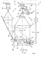
- Fig. 1 is a schematic illustration of a system 1 which is configured to detect, position and inspect an object 3.
- the object 3 is a semi-conductor wafer having a wafer surface 5 provided on a substrate 7.
- the wafer surface may carry structures manufactured by lithographic processes, and the wafer surface 5 may be covered by layers such as resist layers or protective layers applied to the surface during manufacturing steps of the semi-conductor structures.
- the system 1 includes optics providing an imaging beam path, a bright field illumination beam path and a dark field illumination beam path.
- the illustration of these beam paths in Fig. 1 and in the following description is simplified and sufficiently detailed as necessary for illustrating the present exemplary embodiment.
- a more detailed description of suitable optics which can be used in the illustrated example is disclosed in WO 2009/121628 A2 , the disclosure of which is incorporated herein by reference.
- the optics 11 of the system 1 provides an imaging beam path 13 used for imaging an object plane 15 in which the surface 5 of the wafer 3 can be positioned onto a light sensitive substrate 17 of a detector 19.
- the imaging beam path 11 is provided by an objective lens 21 which may be composed of one or more lens elements, a lens 23 which can be composed of one or more lens elements, and a lens 25 which can be composed of one or more lens elements.
- the imaging beam path 11 has a main axis 27 which is, in the present example, oriented orthogonal to the object plane 15.
- the optics 11 further provides a bright field illumination beam path 31 from a light source 33 to the object plane 15.
- the bright field illumination beam path 31 is provided by a lens 35 which can be composed of one or more lens elements, a semi-transparent mirror 37 which is traversed by the imaging beam path 13 and which folds the bright field illumination beam path 31, and the lenses 23 and 21 which are also traversed by the imaging beam path 13.
- a semitransparent mirror can be traversed by the bright field illumination beam path while the imaging beam path is folded by the semitransparent mirror.
- the bright field illumination light is incident on the object 3, which is a semiconductor wafer in the present example, and retroreflecting surface portions 41.
- the retroreflecting surface portions 41 are configured and positioned such that they are located farther away from the light sensitive substrate 17 of the camera 19 and the light source 13 than the object plane 15, wherein distances between the object plane 15 and the surface portions 41 is measured along the imaging beam path 13 and/or the bright field illumination beam path 31, respectively, i.e. along the direction of the main axis 27 of the imaging beam path or a main axis 28 of the bright field illumination beam path.
- the retroreflecting surface portions 41 are fixedly attached to the base 59 of the stage 49.
- the main axis 28 of the bright field illumination beam path 31 is oriented orthogonal to the object plane 15 in the illustrated example, and it also substantially coincides with the main axis 27 of the imaging beam path 13. According to other examples, a small angle of less than 5°, less than 2°, or less than 1° can be included between the main axes 27, 28 of the imaging beam path 13 and the bright field illumination beam path 31, respectively.
- the wafer 3 is supported by a wafer mount 45.
- the wafer mount 45 may carry the wafer 3 by supporting its back surface, wherein the wafer 3 rests on the wafer mount 45 and is attached thereto due to its own gravity and friction.
- the wafer mount 45 may include fingers which are attached to an edge 8 of the wafer 3.
- An example of another wafer mount which could be used in the present example is shown in US 2003/0085368 A1 .
- the wafer mount 45 is supported by a component 47 of a stage 49, wherein the wafer mount 45 is rotable relative to the component 47 about an axis 51 as indicated by an arrow 52.
- An actuator 53 such as a motor or a piezoelectric actuator, is provided for controlling a rotary motion of the wafer mount 45 relative to component 47 of the stage 49.
- the actuator 53 is controlled by a controller 55 via a control line 57.
- the component 47 of the stage 49 is supported by a base 59 of the stage 49 wherein the component 47 can be displaced relative to the base 59 in a direction transverse to the main axes 27, 28, of the imaging beam path 13 and bright field illumination beam path 31, respectively.
- An actuator 61 such as a motor or piezoelectric actuator, is provided to displace the component 47 relative to the base 59 as indicated by an arrow 63.
- the actuator 61 is controlled by the controller 55 via a control line 64.
- the system 1 may comprise a further intermediary component, which is not shown in Fig. 1 , between component 47 and base 59 to displace the wafer mount 45 in a further direction transverse to the direction 63 and axis 51 such that the wafer can be displaced in two non-collinear directions transverse to the main axis 27 and 28 and rotated about axis 51 which is transverse to the two directions of displacement.
- a further intermediary component which is not shown in Fig. 1
- the system 1 may comprise a further intermediary component, which is not shown in Fig. 1 , between component 47 and base 59 to displace the wafer mount 45 in a further direction transverse to the direction 63 and axis 51 such that the wafer can be displaced in two non-collinear directions transverse to the main axis 27 and 28 and rotated about axis 51 which is transverse to the two directions of displacement.
- the controller 55 generates control signals for the actuators 53, 61 based on images recorded by the camera 19 and transmitted to the controller via a control line 67.
- the controller 55 analyses the recorded image to detect the wafer edge 8 and/or a wafer notch as illustrated in more detail below. Based on the detected wafer edge and/or wafer notch it is possible to determine, for example, a center of the wafer and an orientation of the wafer relative to a coordinate system of the system 1. It is then possible to determine, for example, a mapping between a coordinate system of the wafer which may be defined relative to its center and notch and the coordinate system of the system 1.
- the controller may analyse the image recorded by the camera 19 for defects and deteriorations on the wafer surface 5 and map coordinates of the defects and deteriorations as detected in the coordinate system of the system 1 to the coordinate system of the wafer. The controller may then output coordinates of the defects defected in the coordinate system of the wafer.
- the optics 11 further provides a dark field illumination beam path 71 from a dark field illumination light source 73 to the object plane 15, wherein the dark field illumination beam path is provided by a collimating lens 75 which can be composed of one or more lens elements and an objective lens 77 which can be composed of one or more lens elements and a mirror 79.
- a main axis 81 of the dark field illumination beam path 71 is oriented at the object plane 15 under an angle ⁇ relative to the main axis 27 of the imaging beam path 13.
- the angle ⁇ can be greater than 5° or greater than 10° and is about 45° in the illustrated embodiment. Other embodiments may use even larger angles ⁇ , such as 60°.
- Images of the wafer surface can be recorded by the camera 19 either under bright field illumination if the bright field light source 33 supplies light to the wafer surface, or under dark field illumination if the dark field light source 73 supplies light to the wafer surface. Images recorded under bright field illumination and under dark field illumination provide complementary sources of information about defects and deteriorations located on the wafer and which can be analysed and located by the controller 55 and mapped to the coordinate system of the wafer.
- Fig. 2 illustrates a retroreflecting property of the surface portions 41.
- Reference numeral 81 in Fig. 2 designates a collimated beam of light incident on a location 83 on the surface of the surface portion 41.
- the beam of light 81 is incident on the surface portion 41 under an angle ⁇ relative to a direction 85 oriented orthogonal to the surface 41.
- Arrows 87 in Fig. 2 represent intensities of light reflected from the surface 41 at location 83.
- the light is reflected into different directions with different intensities.
- An envelope line 89 represents a distribution of the reflected light in dependence of the angle relative to the surface normal 85.
- a direction of maximum intensity of the reflected light is represented in Fig. 2 by an arrow 87'.
- the arrow 87' is oriented relative to the surface normal 85 under an angle ⁇ which is smaller than the angler ⁇ but greater than 0.
- an angle between the direction of incidence and the orientation of the maximum intensity is smaller than 0,9 ⁇ .
- the angular distribution 89 of the reflected light intensities is different from an angular distribution of reflected intensities provided by a mirror or provided by a surface following Lambert's law.
- the angle ⁇ is substantially smaller than the angle ⁇ for illustrative purposes.
- the angle ⁇ is equal to or only slightly smaller than the angle ⁇ for values of ⁇ of 5°, 10° or even greater values of ⁇ .
- the arrow 87' is located in the same quadrant or on the same side with respect to the surface normal 85 as the direction of the incident light.
- between the direction of incidence of the light beam 81 and the direction of the maximum intensity 87' of the reflected light is smaller than the angle ⁇ between the direction of incidence of the light beam 81 and the surface normal 85 of the surface portion 41.
- the retroreflective surface portions 41 used in the present example can be provided by various retroreflective materials.
- retroreflective materials can be used which are supplied by the 3MTM company under the tradename ScotchLightTM.
- Fig. 3 illustrates a detail of the system shown in Fig. 1 .
- Cones 91 in Fig. 3 represent illumination light beam bundles and imaging beam bundles focused on the object plane 15 at and originating from the object plane at exemplary locations 98, wherein an opening angle 2 ⁇ of the cones 91 correspond to two times a numerical aperture NA of the bright field illumination beam path 31 and the imaging beam path 13 on the side of the object plane 15.
- the light of the beam bundles 91 of the illumination beam path converges above the object plane 15 and diverges below the object plane 15.
- the retroreflecting surface portion 41 is located at a distance ⁇ d from the object plane 15 such that bright field illumination light is incident on a portion 93 of the surface portion 41 and such that the wafer 3 shadows a portion 94 of the retroreflecting surface portion 41 such that bright field illumination light is not incident on the portion 94.
- Reference numeral 95 indicates individual retroreflectors provided on the surface portion 41.
- the individual retroreflectors can be formed by beads or prisms of a material having a high refractive index embedded in a reflecting material or by other configurations.
- Fig. 3 shows a low number of exemplary retroreflectors 95 for illustrative purposes.
- the number of retroreflectors per unit area can be high. For example, more than 10, more than 100, more than 1.000 or mare than 10.000 retroreflectors can be provided per cm 2 of the retroreflecting surface 41.
- the wafer 3 Due to the fact that the wafer 3 has a certain thickness and possibly due to other limitations of the wafer mount 45, it is not possible to position the retroreflecting surface portion 41 in the object plane 15 or immediately below the object plane, and the distance ⁇ d has to be provided between the surface portion 41 and the object plane 15 to allow for the overlap between the wafer 3 and the retroreflecting surface portion 41 such that the wafer shadows the portion 94 of the retroreflecting surface portion 41 when seen from the camera 19.
- the shadow of the wafer 3 defined by the wafer edge 8 formed on the retroreflecting surface portion 41 is not sharply defined since the light cones 91 diverge below the object plane 15.
- the controller 55 is configured such that it detects the wafer edge and/or wafer notch based on an image analysis of the light reflected back from the surface 41. If the surface 41 was formed by a mirror material or a material which is described by Lambert's law, the detected light intensity would gradually rise from 0 to the maximum reflected intensity with increasing distance from the wafer edge. It is possible to determine a location of a wafer edge or notch based on such gradually increasing light intensity. However, such determination of the location would be inaccurate and significantly depend on the distance ⁇ d and the model chosen to simulate the gradually increasing light intensity.
- retroreflective material is provided at the distance ⁇ d from the object plane 15, and arrows 97 represent retroreflected light rays originating from two light cones 91 focused at two exemplary locations 98. It is apparent that the light is reflected back in itself such that the light reflected back and received and accepted by the objective lens 21 appears to substantially originate from the locations 98 on the object plane 15 even though the light originating from a location 98 was reflected back at the retroreflective surface 41 from plural retroreflectors extending over a distance u.
- ⁇ d can be greater than 2 mm, greater than 10 mm or even greater.
- the retroreflecting surface 41 can be located outside of a depth of field of an imaging optics used for the imaging.
- Fig. 4 is an illustration of an elevational view of the wafer 3 and retroreflective surface portions 41 within a field of view 100 as seen from the camera 19.
- a position of the wafer edge 8 can be precisely determined in a coordinate system 101 of the system 1 by an analysis of images recorded by the camera 19. Based on the wafer edge, it is possible to determine a center 103 of the wafer which does not necessarily coincide with a center 105 of the coordinate system 101 and is spaced apart from the center 105 by a distance ⁇ x in the horizontal direction and a distance ⁇ y in the vertical direction.
- one of the retroreflecting surface portions 41 is located on the stage 49 such that it coincides with an expected location of the wafer notch 109 when the wafer is positioned as expected on the wafer mount 45.
- the notch portion of the wafer shadows a portion of the retroreflective portion 41 and that a position of the wafer notch 49 can be precisely determined from an analysis of an image recorded by the camera 19.
- the position of the wafer notch determines an orientation ⁇ of the wafer relative to the coordinate system 101 which may deviate from a desired orientation ⁇ ' by a difference angle ⁇ .
- the controller 55 may drive the actuators 53 and 61 such that the center of the wafer coincides with the center of the coordinate system 101 and such that ⁇ vanishes.
- the wafer is optimally oriented relative to the system 1 and the imaging beam path such that the camera 19 may record an image of the waver surface which allows a precised determination of coordinate of defects and deteriorations on the wafer in the coordinate system of the wafer itself.
- FIG. 1 A further embodiment of an object mount and stage which can be used in the system illustrated with reference to Figs. 1 to 4 above will be illustrated with reference to Figs. 5 to 9 below.
- Fig. 5 is an elevational view of a 300 m wafer 3a mounted on a wafer mount 45a wherein a portion of the wafer 3a is broken away to show details of the wafer mount 45a.
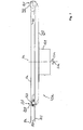
- Fig. 7 is a side view of the wafer mount 45a, and Figs. 8 and 9 show details VIII and IX of Figs. 5 and 7 , respectively.
- the wafer 3a is attached to the wafer mount 45a by three attachment structures 121.
- the attachment structures 121 each comprise a nose portion 123 abutting on a back surface 4a of the wafer, and a lateral grip portion 125 abutting on the wafer edge 8a.
- the nose portion 123 and the grip portion 125 have a fixed relation to each other and can be integrally formed of one piece.
- One attachment structure 121 which is shown in Fig. 9 in detail has the attachment structure 121 configured such that the nose portion 123 is fixed relative to a support 127 carrying the three attachment structures 121 while the grip portion 125 can be displaced relative to the support 127 in a lateral direction as indicated by an arrow 129 shown in Fig. 9 .
- the displacement of the grip portion 125 relative to the support 127 is controlled by an actuator (not shown in Fig. 9 ) which can be operated to release the wafer and to grip the wafer 3a by applying a force to the wafer edge 8a.
- the support 127 is carried by a bearing 129 received by a component 47a of a wafer stage 49a.
- the component 47a and bearing 129 include a motor, such as a piezoelectric motor, to rotate the support 127 and wafer 3a about an axis 51a relative to the component 47a, as indicated by an arrow 52a in Figs. 5 and 7 .
- the component 47a is mounted on a carriage 131 allowing displacement of the component 47 relative to a base 59a of the stage 49a in an inclined direction as illustrated by an arrow 133 in Fig. 6 .
- the displacement in direction 133 is controlled by a motor, such as a piezoelectric motor.
- the carriage 131 is mounted on a component 135 which can be displaced relative to the base 59a in a horizontal direction as indicated by an arrow 137 in Fig. 5 .
- the displacement in the direction 137 is controlled by a motor, such as a piezoelectric motor.
- a movement of the component 47a relative to the carriage in the direction 133 does also result in a horizontal displacement of the wafer 3a relative to the base 59a.
- By controlling the respective motors for displacement in the directions 133 and 137 it is possible to achieve a controlled displacement of the wafer 3a relative to the base in two orthogonal horizontal directions, and the wafer 3a can also be rotated relative to the base 59 about the axis 51a.
- the support 127 carries a ring 141 having a top surface 143 on which a retroreflective material is applied to provide a ring shaped retroreflective surface portion 41a.
- the retroreflective surface portion 41a is configured such that, when seen from above in the elevational view of Fig. 5 , it extends beyond the wafer edge 8a.
- a camera onto which the wafer surface 5a and retroreflective surface portion 41a are imaged will then be able to precisely detect the wafer edge 8a relative to the detected image.
- a notch 109a of the wafer 3a can be detected by the camera if the notch is positioned above the ring shaped surface portion 41a carried by the ring 141. Therefore, it is possible to determine an orientation of the wafer 3a relative to the camera by analysing the detected image as illustrated above.
- the retroreflective surface portion 41a attached to the ring 141 does not extend completely around the periphery of the wafer 3a due to the presence of the three attachment structures 121. This has a consequence that the wafer notch 109a can not be detected based on light retroreflected from the retroreflective surface portions 41a carried by the ring 141, if the wafer notch happens to be positioned such that it is close to one of the attachment structures 121.
- a surface portion 147 close to the nose portion 123 of each attachment structure 121 carries retroreflective material to provide a retroreflective surface 41a'.
- Fig. 8 illustrates a situation where the wafer 3a is oriented such that the wafer notch 109a coincides with one of the attachment structures 121.
- Light reflected back from the retroreflective surface portion 41a' and recorded by the camera allows determination of a position of the notch 109a within the detected image.
- the orientation of the wafer 3a within the image can be determined also in situations whether wafer notch 100a coincides with the wafer attachment structures 121, accordingly.
- Fig. 10 is a schematic illustration similar to Fig. 2 , wherein a surface normal 85b of a retroreflective surface portion 41b is oriented under an angle ⁇ relative to a direction 27b of an imaging beam path. Due to the retroreflective property of the surface portion 41b, a significant portion of incident dark field illumination light 81b is retroreflected back along its direction of incidence. It is, however, possible that a portion of the incident light experiences diffuse scattering at the surface portion 41b. Arrow 151 in Fig. 10 illustrates an exemplary ray of light which is diffusely scattered at the surface portion 41b. This ray of light is incident on a back surface 4b of a wafer 3b and is absorbed at the back surface 4a.
- FIG. 1 A further example of a possibility to reduce an amount of stray light received by a camera in a dark field illumination mode is illustrated with reference to Fig. 1 below. Due to the retroreflective property of the retroreflective surface portion 41, a predominant amount of dark field illumination light incident on the surface portion 41 is retroreflected back towards the dark field illumination light source 73 as indicated by an arrow 159 in Fig. 1 . A portion of the incident dark field illumination light can be still diffusely scattered at the surface portion 41. This portion of stray light could finally reach the camera 19, possibly after one or more reflections at other structures of the system 1.
- the retroreflective material 41 it is possible to configure the retroreflective material 41 such that it reflects back only light from within a narrow wavelength range, such as a wavelength range from 400 nm to 450 nm. Incident light of wavelengths outside of the narrow wavelength range is substantially absorbed by the retroreflective surface portion 49.
- a blocking filter 157 is disposed in the imaging beam path 13 upstream of the camera 19.
- the blocking filter 157 is configured such that it blocks light from within the narrow wavelength range and allows light outside the wavelength range to traverse the filter 157.
- the camera 19 will not receive stray light generated by dark field illumination light incident on the retroreflective surface portions 41, accordingly.
- the system 1 comprises an actuator 161 configured to displace the filter 157 from a position within the imaging beam path 13 to a position outside of the imaging beam path as indicated by an arrow 163 in Fig. 1 .
- the filter 157 is moved to its position outside of the beam path, if the position of the wafer 3 is to be determined from an image recorded by the camera 19 under bright field illumination.
- the light retroreflected back from the retroreflective surface portions 41 within the narrow wavelength range can be received by the camera since the filter 157 is no longer disposed in the beam path upstream of the camera 19.
- Fig. 11 is a flow-chart illustrating a wafer inspection method.
- a wafer is placed on a wafer mount by a suitable wafer handler in a step 201.
- Light is directed towards the wafer and retroreflectors in a step 203.
- Light received from the wafer and the retroreflectors is recorded as an image in a step 205.
- the recorded image is analysed to detect a wafer edge and a wafer notch in a step 207.
- a center of the wafer and an orientation of the wafer is determined in a step 209.
- the determined wafer edge and orientation of the notch is compared with a requirement in a step 211.
- step 211 If the comparison reveals that the position of the wafer center and the orientation of the wafer do not fulfil the requirement, the position and orientation of the wafer is corrected via actuators in a step 213 and a processing according to steps 203, 205, 207, 209 and 211 is repeated. If the determination in step 211 reveals that the wafer center and orientation fulfil the requirement, an image of the wafer is recorded in the step 215. The image is analysed in a step 217 to determine locations of defects of the wafer in a coordinate system of the wafer.
Landscapes
- Physics & Mathematics (AREA)
- Health & Medical Sciences (AREA)
- Life Sciences & Earth Sciences (AREA)
- Chemical & Material Sciences (AREA)
- Analytical Chemistry (AREA)
- Biochemistry (AREA)
- General Health & Medical Sciences (AREA)
- General Physics & Mathematics (AREA)
- Immunology (AREA)
- Pathology (AREA)
- Investigating Materials By The Use Of Optical Means Adapted For Particular Applications (AREA)
- Testing Or Measuring Of Semiconductors Or The Like (AREA)
- Container, Conveyance, Adherence, Positioning, Of Wafer (AREA)
Priority Applications (3)
| Application Number | Priority Date | Filing Date | Title |
|---|---|---|---|
| EP09015996A EP2339331A1 (fr) | 2009-12-23 | 2009-12-23 | Systèmes et procédés de positionnement et d'inspection |
| PCT/EP2010/007925 WO2011076429A1 (fr) | 2009-12-23 | 2010-12-23 | Système et procédé d'inspection de tranche semiconductrice |
| US13/518,349 US9182357B2 (en) | 2009-12-23 | 2010-12-23 | Semiconductor wafer inspection system and method |
Applications Claiming Priority (1)
| Application Number | Priority Date | Filing Date | Title |
|---|---|---|---|
| EP09015996A EP2339331A1 (fr) | 2009-12-23 | 2009-12-23 | Systèmes et procédés de positionnement et d'inspection |
Publications (1)
| Publication Number | Publication Date |
|---|---|
| EP2339331A1 true EP2339331A1 (fr) | 2011-06-29 |
Family
ID=42167703
Family Applications (1)
| Application Number | Title | Priority Date | Filing Date |
|---|---|---|---|
| EP09015996A Withdrawn EP2339331A1 (fr) | 2009-12-23 | 2009-12-23 | Systèmes et procédés de positionnement et d'inspection |
Country Status (3)
| Country | Link |
|---|---|
| US (1) | US9182357B2 (fr) |
| EP (1) | EP2339331A1 (fr) |
| WO (1) | WO2011076429A1 (fr) |
Cited By (2)
| Publication number | Priority date | Publication date | Assignee | Title |
|---|---|---|---|---|
| WO2017215924A1 (fr) * | 2016-06-13 | 2017-12-21 | Asml Netherlands B.V. | Procédés et appareil permettant de déterminer la position d'une structure cible sur un substrat, procédés et appareil permettant de déterminer la position d'un substrat |
| WO2023030814A1 (fr) * | 2021-09-03 | 2023-03-09 | Asml Netherlands B.V. | Procédé et système de détection d'arête d'échantillon et positionnement d'image pour appareil d'inspection d'image |
Families Citing this family (15)
| Publication number | Priority date | Publication date | Assignee | Title |
|---|---|---|---|---|
| US20130120557A1 (en) * | 2011-11-14 | 2013-05-16 | Microscan Systems, Inc. | Part inspection system |
| US9796045B2 (en) * | 2013-12-19 | 2017-10-24 | Sunpower Corporation | Wafer alignment with restricted visual access |
| KR101882823B1 (ko) * | 2013-12-31 | 2018-07-27 | 상하이 마이크로 일렉트로닉스 이큅먼트(그룹) 컴퍼니 리미티드 | 실리콘 웨이퍼 프리 얼라인 장치 및 그 방법 |
| WO2015135782A1 (fr) * | 2014-03-12 | 2015-09-17 | Asml Netherlands B.V. | Système de capteur, système de manipulation de substrat et appareil lithographique |
| SE537979C2 (sv) * | 2014-04-07 | 2016-01-05 | Optonova Sweden Ab | Förfarande för produktkontroll med kamera och belysningsanordning |
| US9506873B2 (en) * | 2014-04-15 | 2016-11-29 | Kla-Tencor Corp. | Pattern suppression in logic for wafer inspection |
| JP7034797B2 (ja) * | 2018-03-28 | 2022-03-14 | 株式会社東京精密 | 貼り合せ基板の測定方法および加工方法並びにそれらに用いる装置 |
| US10978331B2 (en) * | 2018-03-30 | 2021-04-13 | Taiwan Semiconductor Manufacturing Co., Ltd. | Systems and methods for orientator based wafer defect sensing |
| US12211723B2 (en) * | 2018-04-24 | 2025-01-28 | Disco Hi-Tec Europe Gmbh | Alignment device and alignment method |
| US11295975B2 (en) * | 2019-09-13 | 2022-04-05 | Brooks Automation Us, Llc | Method and apparatus for substrate alignment |
| CN114509446B (zh) * | 2020-10-23 | 2025-07-25 | 联华电子股份有限公司 | 晶片缺角自动检测方法与晶片缺角自动检测系统 |
| US12051604B2 (en) * | 2021-01-06 | 2024-07-30 | Samsung Electronics Co., Ltd. | Apparatus for manufacturing semiconductor device and method of manufacturing semiconductor device |
| CN114951037A (zh) * | 2022-04-13 | 2022-08-30 | 泉州师范学院 | 半导体晶粒四面同时等光程成像检测装置与方法 |
| CN115561261B (zh) * | 2022-11-14 | 2023-02-03 | 昂坤视觉(北京)科技有限公司 | 侧边检测设备及其光学检测方法 |
| CN115714103B (zh) * | 2022-11-25 | 2023-11-24 | 拓荆键科(海宁)半导体设备有限公司 | 用于晶圆键合对准及检测的装置和方法 |
Citations (5)
| Publication number | Priority date | Publication date | Assignee | Title |
|---|---|---|---|---|
| DE1083065B (de) * | 1955-01-14 | 1960-06-09 | Zeiss Carl Fa | Einrichtung zur wahlweisen Erzielung einer Durch- und Auflichtbelichtung eines Objektes |
| US20030133133A1 (en) * | 2002-01-09 | 2003-07-17 | Dainippon Screen Mfg. Co., Ltd. | Measuring apparatus |
| DE10254542A1 (de) * | 2002-07-01 | 2004-01-22 | Hottinger Maschinenbau Gmbh | Vorrichtung und Verfahren zur Detektion der Kontur beliebiger Teile, insbesondere von Gussteilen |
| WO2006048857A1 (fr) * | 2004-11-01 | 2006-05-11 | Cognitens Ltd. | Procede et systeme de mesure de contour optique |
| US20070058168A1 (en) * | 2005-09-14 | 2007-03-15 | Cognex Technology And Investment Corporation | Method and Apparatus for Backlighting a Wafer during Alignment |
Family Cites Families (5)
| Publication number | Priority date | Publication date | Assignee | Title |
|---|---|---|---|---|
| JP4514942B2 (ja) * | 2000-12-07 | 2010-07-28 | 株式会社アルバック | 成膜装置 |
| US6900451B2 (en) | 2001-11-08 | 2005-05-31 | Multimextrixs, Llc | Mapping sensor system for detecting positions of flat objects |
| US20080021665A1 (en) * | 2006-07-20 | 2008-01-24 | David Vaughnn | Focusing method and apparatus |
| DE102006059190B4 (de) | 2006-12-15 | 2009-09-10 | Vistec Semiconductor Systems Gmbh | Vorrichtung zur Wafer-Inspektion |
| CN102016554B (zh) | 2008-04-04 | 2013-01-30 | 南达技术公司 | 光学检验系统及方法 |
-
2009
- 2009-12-23 EP EP09015996A patent/EP2339331A1/fr not_active Withdrawn
-
2010
- 2010-12-23 US US13/518,349 patent/US9182357B2/en active Active
- 2010-12-23 WO PCT/EP2010/007925 patent/WO2011076429A1/fr not_active Ceased
Patent Citations (5)
| Publication number | Priority date | Publication date | Assignee | Title |
|---|---|---|---|---|
| DE1083065B (de) * | 1955-01-14 | 1960-06-09 | Zeiss Carl Fa | Einrichtung zur wahlweisen Erzielung einer Durch- und Auflichtbelichtung eines Objektes |
| US20030133133A1 (en) * | 2002-01-09 | 2003-07-17 | Dainippon Screen Mfg. Co., Ltd. | Measuring apparatus |
| DE10254542A1 (de) * | 2002-07-01 | 2004-01-22 | Hottinger Maschinenbau Gmbh | Vorrichtung und Verfahren zur Detektion der Kontur beliebiger Teile, insbesondere von Gussteilen |
| WO2006048857A1 (fr) * | 2004-11-01 | 2006-05-11 | Cognitens Ltd. | Procede et systeme de mesure de contour optique |
| US20070058168A1 (en) * | 2005-09-14 | 2007-03-15 | Cognex Technology And Investment Corporation | Method and Apparatus for Backlighting a Wafer during Alignment |
Cited By (6)
| Publication number | Priority date | Publication date | Assignee | Title |
|---|---|---|---|---|
| WO2017215924A1 (fr) * | 2016-06-13 | 2017-12-21 | Asml Netherlands B.V. | Procédés et appareil permettant de déterminer la position d'une structure cible sur un substrat, procédés et appareil permettant de déterminer la position d'un substrat |
| US10444647B2 (en) | 2016-06-13 | 2019-10-15 | Asml Netherlands B.V. | Methods and apparatus for determining the position of a target structure on a substrate, methods and apparatus for determining the position of a substrate |
| WO2023030814A1 (fr) * | 2021-09-03 | 2023-03-09 | Asml Netherlands B.V. | Procédé et système de détection d'arête d'échantillon et positionnement d'image pour appareil d'inspection d'image |
| TWI838822B (zh) * | 2021-09-03 | 2024-04-11 | 荷蘭商Asml荷蘭公司 | 用於樣本邊緣偵測之方法和系統及用於影像檢測設備之樣本定位 |
| US20240402093A1 (en) * | 2021-09-03 | 2024-12-05 | Asml Netherlands B.V. | Method and system of sample edge detection and sample positioning for image inspection apparatus |
| US12560556B2 (en) * | 2021-09-03 | 2026-02-24 | Asml Netherlands B.V. | Method and system of sample edge detection and sample positioning for image inspection apparatus |
Also Published As
| Publication number | Publication date |
|---|---|
| US20120268585A1 (en) | 2012-10-25 |
| US9182357B2 (en) | 2015-11-10 |
| WO2011076429A1 (fr) | 2011-06-30 |
Similar Documents
| Publication | Publication Date | Title |
|---|---|---|
| EP2339331A1 (fr) | Systèmes et procédés de positionnement et d'inspection | |
| TWI589861B (zh) | 偵測晶圓中裂痕的系統與方法 | |
| KR102235580B1 (ko) | 반도체 웨이퍼 검사를 위한 결함 마킹 | |
| JP5860044B2 (ja) | 視覚画像化および赤外画像化を行なう荷電粒子ビーム処理システム | |
| EP1156321B1 (fr) | Procede de controle d'une surface a analyser et analyseur de surface a balayage | |
| US20250309000A1 (en) | Laser processing method, semiconductor device manufacturing method, and examination device | |
| TWI673487B (zh) | 度量系統、度量設備及度量方法 | |
| CN110073203B (zh) | 检查透明基材上的缺陷的方法和设备 | |
| JP3709431B2 (ja) | 微細構造化表面での角度依存回折効果の高速測定装置 | |
| TW202246733A (zh) | 用於量測平面粗度及/或瑕疵的量測裝置及方法 | |
| KR102542405B1 (ko) | 재귀반사 표면을 이용한 가공물의 위치, 배향, 및 스케일의 검출 | |
| US20130330848A1 (en) | Observation device, inspection device, method for manufacturing semiconductor device, and substrate support member | |
| WO2009112704A1 (fr) | Dispositif d'inspection de plaquettes semi-conductrices | |
| US9355919B2 (en) | Methods and systems for inspecting bonded wafers | |
| EP3201611A1 (fr) | Inspection de bord de tranche avec profil de bord suivant une trajectoire | |
| CN104423147B (zh) | 检查装置及检查方法 | |
| JP7183156B2 (ja) | 透明基板上の欠陥部の検査方法および装置並びに入射光の出射方法 | |
| TW202438874A (zh) | 半導體邊緣及斜角檢驗工具系統 | |
| TW200949236A (en) | Foreign particle inspection apparatus, exposure apparatus, and method of manufacturing semiconductor device | |
| US11450576B2 (en) | Laser processing method, method for manufacturing semiconductor device, and inspecting device | |
| KR102637333B1 (ko) | 웨이퍼 검사 광학계 | |
| TWI515422B (zh) | 半導體晶圓檢驗系統和方法 | |
| JP4974267B2 (ja) | ウェーハ外周検査方法 | |
| CN108109934B (zh) | 检测金属层表面的颗粒的方法 | |
| WO2021220456A1 (fr) | Système de traitement |
Legal Events
| Date | Code | Title | Description |
|---|---|---|---|
| PUAI | Public reference made under article 153(3) epc to a published international application that has entered the european phase |
Free format text: ORIGINAL CODE: 0009012 |
|
| AK | Designated contracting states |
Kind code of ref document: A1 Designated state(s): AT BE BG CH CY CZ DE DK EE ES FI FR GB GR HR HU IE IS IT LI LT LU LV MC MK MT NL NO PL PT RO SE SI SK SM TR |
|
| AX | Request for extension of the european patent |
Extension state: AL BA RS |
|
| 17P | Request for examination filed |
Effective date: 20111229 |
|
| 17Q | First examination report despatched |
Effective date: 20181012 |
|
| STAA | Information on the status of an ep patent application or granted ep patent |
Free format text: STATUS: THE APPLICATION IS DEEMED TO BE WITHDRAWN |
|
| 18D | Application deemed to be withdrawn |
Effective date: 20190223 |