EP2339641A2 - Cellule solaire à film mince à semiconducteur composé, procédé de fabrication d'une cellule solaire et panneau solaire à film mince à semiconducteur composé - Google Patents
Cellule solaire à film mince à semiconducteur composé, procédé de fabrication d'une cellule solaire et panneau solaire à film mince à semiconducteur composé Download PDFInfo
- Publication number
- EP2339641A2 EP2339641A2 EP10172010A EP10172010A EP2339641A2 EP 2339641 A2 EP2339641 A2 EP 2339641A2 EP 10172010 A EP10172010 A EP 10172010A EP 10172010 A EP10172010 A EP 10172010A EP 2339641 A2 EP2339641 A2 EP 2339641A2
- Authority
- EP
- European Patent Office
- Prior art keywords
- thin film
- compound thin
- solar cell
- buffer layer
- film solar
- Prior art date
- Legal status (The legal status is an assumption and is not a legal conclusion. Google has not performed a legal analysis and makes no representation as to the accuracy of the status listed.)
- Withdrawn
Links
- 150000001875 compounds Chemical class 0.000 title claims description 70
- 239000010409 thin film Substances 0.000 title claims description 70
- 239000004065 semiconductor Substances 0.000 title claims description 31
- 238000004519 manufacturing process Methods 0.000 title claims description 14
- GWEVSGVZZGPLCZ-UHFFFAOYSA-N Titan oxide Chemical compound O=[Ti]=O GWEVSGVZZGPLCZ-UHFFFAOYSA-N 0.000 claims abstract description 83
- 229910052758 niobium Inorganic materials 0.000 claims abstract description 31
- 229910052715 tantalum Inorganic materials 0.000 claims abstract description 31
- MCMNRKCIXSYSNV-UHFFFAOYSA-N Zirconium dioxide Chemical compound O=[Zr]=O MCMNRKCIXSYSNV-UHFFFAOYSA-N 0.000 claims abstract description 30
- YBMRDBCBODYGJE-UHFFFAOYSA-N germanium dioxide Chemical compound O=[Ge]=O YBMRDBCBODYGJE-UHFFFAOYSA-N 0.000 claims abstract description 20
- 229910002113 barium titanate Inorganic materials 0.000 claims abstract description 18
- 229910017676 MgTiO3 Inorganic materials 0.000 claims abstract description 14
- 229910002370 SrTiO3 Inorganic materials 0.000 claims abstract description 12
- 229910002971 CaTiO3 Inorganic materials 0.000 claims abstract description 11
- CJNBYAVZURUTKZ-UHFFFAOYSA-N hafnium(IV) oxide Inorganic materials O=[Hf]=O CJNBYAVZURUTKZ-UHFFFAOYSA-N 0.000 claims abstract description 10
- 239000000758 substrate Substances 0.000 claims description 30
- 238000000137 annealing Methods 0.000 claims description 21
- 239000010408 film Substances 0.000 claims description 20
- 239000002243 precursor Substances 0.000 claims description 10
- 239000006059 cover glass Substances 0.000 claims description 7
- 238000007789 sealing Methods 0.000 claims description 6
- 229920005989 resin Polymers 0.000 claims description 5
- 239000011347 resin Substances 0.000 claims description 5
- -1 CaTiO2 Inorganic materials 0.000 claims description 2
- 239000007787 solid Substances 0.000 claims description 2
- 239000000463 material Substances 0.000 abstract description 54
- 238000010521 absorption reaction Methods 0.000 description 42
- 229910052733 gallium Inorganic materials 0.000 description 32
- 229910052738 indium Inorganic materials 0.000 description 27
- 238000000034 method Methods 0.000 description 25
- 238000004544 sputter deposition Methods 0.000 description 15
- 238000000151 deposition Methods 0.000 description 14
- 239000011521 glass Substances 0.000 description 14
- 239000013078 crystal Substances 0.000 description 13
- 239000007790 solid phase Substances 0.000 description 11
- 238000000224 chemical solution deposition Methods 0.000 description 10
- 239000000654 additive Substances 0.000 description 9
- 230000000996 additive effect Effects 0.000 description 9
- 239000007789 gas Substances 0.000 description 9
- 230000008021 deposition Effects 0.000 description 8
- 238000006243 chemical reaction Methods 0.000 description 7
- 230000000694 effects Effects 0.000 description 7
- 239000012071 phase Substances 0.000 description 7
- 229910052984 zinc sulfide Inorganic materials 0.000 description 7
- 229910052751 metal Inorganic materials 0.000 description 6
- 239000002184 metal Substances 0.000 description 6
- 238000002834 transmittance Methods 0.000 description 6
- 229910052782 aluminium Inorganic materials 0.000 description 5
- 238000002425 crystallisation Methods 0.000 description 5
- 230000008025 crystallization Effects 0.000 description 5
- 238000009792 diffusion process Methods 0.000 description 5
- 238000001004 secondary ion mass spectrometry Methods 0.000 description 5
- 229910052725 zinc Inorganic materials 0.000 description 5
- QVGXLLKOCUKJST-UHFFFAOYSA-N atomic oxygen Chemical compound [O] QVGXLLKOCUKJST-UHFFFAOYSA-N 0.000 description 4
- 238000009413 insulation Methods 0.000 description 4
- 150000002500 ions Chemical class 0.000 description 4
- 229910052760 oxygen Inorganic materials 0.000 description 4
- 239000001301 oxygen Substances 0.000 description 4
- 239000000243 solution Substances 0.000 description 4
- 238000001228 spectrum Methods 0.000 description 4
- XOLBLPGZBRYERU-UHFFFAOYSA-N tin dioxide Chemical compound O=[Sn]=O XOLBLPGZBRYERU-UHFFFAOYSA-N 0.000 description 4
- 238000002441 X-ray diffraction Methods 0.000 description 3
- DQXBYHZEEUGOBF-UHFFFAOYSA-N but-3-enoic acid;ethene Chemical compound C=C.OC(=O)CC=C DQXBYHZEEUGOBF-UHFFFAOYSA-N 0.000 description 3
- 229910052793 cadmium Inorganic materials 0.000 description 3
- 239000005038 ethylene vinyl acetate Substances 0.000 description 3
- 231100000956 nontoxicity Toxicity 0.000 description 3
- 229920001200 poly(ethylene-vinyl acetate) Polymers 0.000 description 3
- 238000010248 power generation Methods 0.000 description 3
- 238000000926 separation method Methods 0.000 description 3
- 229910004613 CdTe Inorganic materials 0.000 description 2
- 229910000807 Ga alloy Inorganic materials 0.000 description 2
- FAPWRFPIFSIZLT-UHFFFAOYSA-M Sodium chloride Chemical compound [Na+].[Cl-] FAPWRFPIFSIZLT-UHFFFAOYSA-M 0.000 description 2
- 238000004833 X-ray photoelectron spectroscopy Methods 0.000 description 2
- 229910021417 amorphous silicon Inorganic materials 0.000 description 2
- 230000004888 barrier function Effects 0.000 description 2
- DVRDHUBQLOKMHZ-UHFFFAOYSA-N chalcopyrite Chemical compound [S-2].[S-2].[Fe+2].[Cu+2] DVRDHUBQLOKMHZ-UHFFFAOYSA-N 0.000 description 2
- 229910052951 chalcopyrite Inorganic materials 0.000 description 2
- 239000000470 constituent Substances 0.000 description 2
- 230000003247 decreasing effect Effects 0.000 description 2
- 230000007850 degeneration Effects 0.000 description 2
- 239000002019 doping agent Substances 0.000 description 2
- 238000001035 drying Methods 0.000 description 2
- 239000004615 ingredient Substances 0.000 description 2
- 230000031700 light absorption Effects 0.000 description 2
- 235000002639 sodium chloride Nutrition 0.000 description 2
- 239000011780 sodium chloride Substances 0.000 description 2
- 239000006104 solid solution Substances 0.000 description 2
- 238000001179 sorption measurement Methods 0.000 description 2
- 238000006467 substitution reaction Methods 0.000 description 2
- 231100000331 toxic Toxicity 0.000 description 2
- 230000002588 toxic effect Effects 0.000 description 2
- 229910002475 Cu2ZnSnS4 Inorganic materials 0.000 description 1
- 206010021143 Hypoxia Diseases 0.000 description 1
- 229910003363 ZnMgO Inorganic materials 0.000 description 1
- 229910052784 alkaline earth metal Inorganic materials 0.000 description 1
- 150000001342 alkaline earth metals Chemical class 0.000 description 1
- 238000004458 analytical method Methods 0.000 description 1
- 229910052796 boron Inorganic materials 0.000 description 1
- WUKWITHWXAAZEY-UHFFFAOYSA-L calcium difluoride Chemical compound [F-].[F-].[Ca+2] WUKWITHWXAAZEY-UHFFFAOYSA-L 0.000 description 1
- 239000000969 carrier Substances 0.000 description 1
- 230000007812 deficiency Effects 0.000 description 1
- 238000005137 deposition process Methods 0.000 description 1
- 230000005684 electric field Effects 0.000 description 1
- 230000002708 enhancing effect Effects 0.000 description 1
- 238000001704 evaporation Methods 0.000 description 1
- 230000002349 favourable effect Effects 0.000 description 1
- 239000010436 fluorite Substances 0.000 description 1
- 238000010438 heat treatment Methods 0.000 description 1
- 231100000086 high toxicity Toxicity 0.000 description 1
- 239000011261 inert gas Substances 0.000 description 1
- 239000012212 insulator Substances 0.000 description 1
- 239000005340 laminated glass Substances 0.000 description 1
- 239000000203 mixture Substances 0.000 description 1
- 230000001473 noxious effect Effects 0.000 description 1
- 230000001376 precipitating effect Effects 0.000 description 1
- 229910052711 selenium Inorganic materials 0.000 description 1
- 230000035945 sensitivity Effects 0.000 description 1
- 229910052709 silver Inorganic materials 0.000 description 1
- 239000005361 soda-lime glass Substances 0.000 description 1
- HUAUNKAZQWMVFY-UHFFFAOYSA-M sodium;oxocalcium;hydroxide Chemical compound [OH-].[Na+].[Ca]=O HUAUNKAZQWMVFY-UHFFFAOYSA-M 0.000 description 1
- 230000003595 spectral effect Effects 0.000 description 1
- 229910052717 sulfur Inorganic materials 0.000 description 1
- GUVRBAGPIYLISA-UHFFFAOYSA-N tantalum atom Chemical compound [Ta] GUVRBAGPIYLISA-UHFFFAOYSA-N 0.000 description 1
- 229910052714 tellurium Inorganic materials 0.000 description 1
- 239000005341 toughened glass Substances 0.000 description 1
- 229910052720 vanadium Inorganic materials 0.000 description 1
- LEONUFNNVUYDNQ-UHFFFAOYSA-N vanadium atom Chemical compound [V] LEONUFNNVUYDNQ-UHFFFAOYSA-N 0.000 description 1
- 238000007740 vapor deposition Methods 0.000 description 1
Images





Classifications
-
- H—ELECTRICITY
- H10—SEMICONDUCTOR DEVICES; ELECTRIC SOLID-STATE DEVICES NOT OTHERWISE PROVIDED FOR
- H10F—INORGANIC SEMICONDUCTOR DEVICES SENSITIVE TO INFRARED RADIATION, LIGHT, ELECTROMAGNETIC RADIATION OF SHORTER WAVELENGTH OR CORPUSCULAR RADIATION
- H10F77/00—Constructional details of devices covered by this subclass
- H10F77/10—Semiconductor bodies
- H10F77/12—Active materials
- H10F77/126—Active materials comprising only Group I-III-VI chalcopyrite materials, e.g. CuInSe2, CuGaSe2 or CuInGaSe2 [CIGS]
-
- H—ELECTRICITY
- H10—SEMICONDUCTOR DEVICES; ELECTRIC SOLID-STATE DEVICES NOT OTHERWISE PROVIDED FOR
- H10F—INORGANIC SEMICONDUCTOR DEVICES SENSITIVE TO INFRARED RADIATION, LIGHT, ELECTROMAGNETIC RADIATION OF SHORTER WAVELENGTH OR CORPUSCULAR RADIATION
- H10F71/00—Manufacture or treatment of devices covered by this subclass
- H10F71/125—The active layers comprising only Group II-VI materials, e.g. CdS, ZnS or CdTe
- H10F71/1257—The active layers comprising only Group II-VI materials, e.g. CdS, ZnS or CdTe comprising growth substrates not made of Group II-VI materials
-
- H—ELECTRICITY
- H10—SEMICONDUCTOR DEVICES; ELECTRIC SOLID-STATE DEVICES NOT OTHERWISE PROVIDED FOR
- H10F—INORGANIC SEMICONDUCTOR DEVICES SENSITIVE TO INFRARED RADIATION, LIGHT, ELECTROMAGNETIC RADIATION OF SHORTER WAVELENGTH OR CORPUSCULAR RADIATION
- H10F71/00—Manufacture or treatment of devices covered by this subclass
- H10F71/127—The active layers comprising only Group III-V materials, e.g. GaAs or InP
- H10F71/1276—The active layers comprising only Group III-V materials, e.g. GaAs or InP comprising growth substrates not made of Group III-V materials
-
- H—ELECTRICITY
- H10—SEMICONDUCTOR DEVICES; ELECTRIC SOLID-STATE DEVICES NOT OTHERWISE PROVIDED FOR
- H10F—INORGANIC SEMICONDUCTOR DEVICES SENSITIVE TO INFRARED RADIATION, LIGHT, ELECTROMAGNETIC RADIATION OF SHORTER WAVELENGTH OR CORPUSCULAR RADIATION
- H10F71/00—Manufacture or treatment of devices covered by this subclass
- H10F71/138—Manufacture of transparent electrodes, e.g. transparent conductive oxides [TCO] or indium tin oxide [ITO] electrodes
-
- H—ELECTRICITY
- H10—SEMICONDUCTOR DEVICES; ELECTRIC SOLID-STATE DEVICES NOT OTHERWISE PROVIDED FOR
- H10F—INORGANIC SEMICONDUCTOR DEVICES SENSITIVE TO INFRARED RADIATION, LIGHT, ELECTROMAGNETIC RADIATION OF SHORTER WAVELENGTH OR CORPUSCULAR RADIATION
- H10F77/00—Constructional details of devices covered by this subclass
- H10F77/10—Semiconductor bodies
- H10F77/12—Active materials
- H10F77/123—Active materials comprising only Group II-VI materials, e.g. CdS, ZnS or HgCdTe
-
- H—ELECTRICITY
- H10—SEMICONDUCTOR DEVICES; ELECTRIC SOLID-STATE DEVICES NOT OTHERWISE PROVIDED FOR
- H10F—INORGANIC SEMICONDUCTOR DEVICES SENSITIVE TO INFRARED RADIATION, LIGHT, ELECTROMAGNETIC RADIATION OF SHORTER WAVELENGTH OR CORPUSCULAR RADIATION
- H10F77/00—Constructional details of devices covered by this subclass
- H10F77/20—Electrodes
- H10F77/244—Electrodes made of transparent conductive layers, e.g. transparent conductive oxide [TCO] layers
-
- Y—GENERAL TAGGING OF NEW TECHNOLOGICAL DEVELOPMENTS; GENERAL TAGGING OF CROSS-SECTIONAL TECHNOLOGIES SPANNING OVER SEVERAL SECTIONS OF THE IPC; TECHNICAL SUBJECTS COVERED BY FORMER USPC CROSS-REFERENCE ART COLLECTIONS [XRACs] AND DIGESTS
- Y02—TECHNOLOGIES OR APPLICATIONS FOR MITIGATION OR ADAPTATION AGAINST CLIMATE CHANGE
- Y02E—REDUCTION OF GREENHOUSE GAS [GHG] EMISSIONS, RELATED TO ENERGY GENERATION, TRANSMISSION OR DISTRIBUTION
- Y02E10/00—Energy generation through renewable energy sources
- Y02E10/50—Photovoltaic [PV] energy
- Y02E10/541—CuInSe2 material PV cells
-
- Y—GENERAL TAGGING OF NEW TECHNOLOGICAL DEVELOPMENTS; GENERAL TAGGING OF CROSS-SECTIONAL TECHNOLOGIES SPANNING OVER SEVERAL SECTIONS OF THE IPC; TECHNICAL SUBJECTS COVERED BY FORMER USPC CROSS-REFERENCE ART COLLECTIONS [XRACs] AND DIGESTS
- Y02—TECHNOLOGIES OR APPLICATIONS FOR MITIGATION OR ADAPTATION AGAINST CLIMATE CHANGE
- Y02E—REDUCTION OF GREENHOUSE GAS [GHG] EMISSIONS, RELATED TO ENERGY GENERATION, TRANSMISSION OR DISTRIBUTION
- Y02E10/00—Energy generation through renewable energy sources
- Y02E10/50—Photovoltaic [PV] energy
- Y02E10/544—Solar cells from Group III-V materials
-
- Y—GENERAL TAGGING OF NEW TECHNOLOGICAL DEVELOPMENTS; GENERAL TAGGING OF CROSS-SECTIONAL TECHNOLOGIES SPANNING OVER SEVERAL SECTIONS OF THE IPC; TECHNICAL SUBJECTS COVERED BY FORMER USPC CROSS-REFERENCE ART COLLECTIONS [XRACs] AND DIGESTS
- Y02—TECHNOLOGIES OR APPLICATIONS FOR MITIGATION OR ADAPTATION AGAINST CLIMATE CHANGE
- Y02P—CLIMATE CHANGE MITIGATION TECHNOLOGIES IN THE PRODUCTION OR PROCESSING OF GOODS
- Y02P70/00—Climate change mitigation technologies in the production process for final industrial or consumer products
- Y02P70/50—Manufacturing or production processes characterised by the final manufactured product
Definitions
- the present invention concerns a technique which is effective for improving the performance of a compound thin film solar cell.
- Compound thin film solar cells include those using, for example, a CuInSe 2 type compound belonging to the I-III-VI 2 group, a CdTe type compound belonging to the II-VI group, and a Cu 2 ZnSnS 4 type compound belonging to the I 2 -II-IV-VI 4 group.
- the cell using the CuInSe 2 type compound belonging to the I-III-VI 2 group is a compound thin film solar cell capable of obtaining the highest energy conversion efficiency at present and attains a high energy conversion efficiency of about 20% in a small area.
- Fig. 1 shows a basic structure of a compound thin film solar cell using the CuInSe 2 type compound belonging to the I-III-VI 2 group.
- a soda lime substrate is usually used for a substrate 1. This is because Na precipitating from the substrate 1 has an effect of improving the crystallinity, etc. of an absorption layer 3 and improving the energy conversion efficiency (Na effect).
- Mo is generally used for a back electrode 2.
- a compound semiconductor having a chalcopyrite type crystal structure typically represented by CuInSe 2 is used for the absorption layer 3.
- the semiconductor compound may be replaced or partially substituted for the ingredient Cu by Ag, in In by Ga or Al, and Se by S or Te, thereby capable of controlling the lattice constant and the band gap.
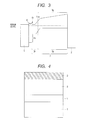
- the band gap is widened by partially substituting In by Ga or Al or partially substituting Se by S. It has been known that diffusion of excited electrons to the back electrode 2 can be suppressed to improve the energy conversion efficiency by modifying the absorption layer 3 to Cu(In, Ga)Se 2 of higher Ga compositional ratio to the back electrode 2 thereby forming a graded structure having a band gap which is widened toward the back electrode 2 by utilizing the band gap controlling function as shown in the band structural view of Fig. 3 .
- band gap of the absorption layer 3 capable of absorbing a solar cell energy and performing photoelectronic conversion most efficiently is 1.4 eV in a case of a unijunction solar cell and 1.75 eV in a case of a top cell of a double junction solar cell, and studies has the now been proceeded for widening the gap of the absorption layer for improving the efficiency.
- a gas phase selenization method of forming a metal thin film by deposition as a precursor by sputtering or vapor deposition, and converting the precursor film into an Se compound by annealing in a hydrogenated Se atmosphere at a high temperature of 500°C or higher is generally used.
- an n-type buffer layer 4 and a transparent electrode 5 are formed.
- an n-type semiconductor thin film comprising CdS (refer to USP No. 4611091 ), ZnS (refer to JP-A-Hei 8(1996)-330614 , ZnO (refer to JP-A-2006-147759 ), etc, formed by a CBD (Chemical Bath Deposition) method, that is, a deposition method in a solution is used.
- a CBD Chemical Bath Deposition
- ITO or ZnO with addition of Al, Ga, or B is used
- the n-type buffer layer 4 at first has a function of forming a pn heterojunction with the absorption layer 3 such as CuInSe 2 as a p-type semiconductor, or diffusing bivalent element ions such as of Cd or Zn as a constituent ingredient into the absorption layer 3 comprising CuInSe 2 , etc. and substituting Cu sites of monovalent element ions to transform the surface of the absorption layer 3 comprising CuInSe 2 , etc.
- the buffer layer 4 has a second function of insulation of preventing direct contact between the absorption layer 3 and the transparent electrode 5 thereby decreasing a component of shunting leak.
- the band offset of the conduction band (energy level difference) 6c is as small as about 0 to +0.4 eV, whereas the band offset of the valence band (energy level difference) 6v is as great as several eV between the n-type buffer layer 4 and the absorption layer 3.
- the buffer layer 4 has a third function as a window layer of in-taking light into the absorption layer 3. It is described that the band offset of the conduction band (energy level difference) 6c is preferably as small as about 0 to +0.4 eV in " Recent development of thin film compound semiconductor photovoltaic cells ", p81 (Published from CMC, on June 30, 2007 ).
- CdS CdS, ZnS, ZnO, etc. formed by a CBD (Chemical Bath Deposition) method as a deposition method in a solution
- CBD Chemical Bath Deposition
- CdS is a material that has been used most frequently so far and has a feature capable of attaining high energy conversion efficiency because diffusion of bivalent Cd is effective as a dopant upon forming a pn homojunction, matching between the CdS conduction band position and the CuInSe 2 conduction band position is favorable, and the conduction band offset 6c is small.
- ZnS or ZnO is a material which has been started to be used generally instead of CdS since noxious Cd is not used.
- the conduction band position is lower than the conduction band position of CuInSe 2 and the band offset of the conduction band 6c is negative tending to lower the open circuit voltage, the output voltage tends to be lowered and the efficiency is somewhat lowered compared with the case of using CdS.
- the conduction band offset can be matched to CuIn 0 . 8 Ga 0 . 2 Se 2 having the band gap of 1.2 eV used mainly at present, they are difficult to cope with the wide gap absorption layer having a band gap of 1.4 to 1.75 eV which have now been under development. Further, as a problem in common with CdS, ZnS, and ZnO, heat resistance is low.
- a CBD (Chemical Bath Deposition) method of deposition in a solution at a temperature of about room temperature to 80°C is used as the production method.
- the current CuInSe 2 type solar cell has a substrate structure as shown Fig.
- the solar cell module of the substrate structure requires a cover glass 8 for protection on the side of the transparent electrode 5
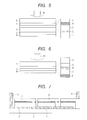
- it has a laminated glass structure of using two sheets of glass including the glass substrate 1 by way of a sealing resin 7 and involves a problem of using more number of sheets of glass and in decreasing the cost compared with the superstrate structure in which the glass substrate 1 also serves as the cover glass 8 adopted in an amorphous Si thin film solar cell as shown in Fig. 6 .
- CBD Cerical Bath Deposition
- the CBD (Chemical Bath Deposition) method which is an existent production method for CdS, ZnS, or ZnO of the buffer layer 4 is a solution process and, since the constitution of apparatus is greatly different from that of the dry process such as sputtering as another method of forming the back electrode 2, the absorption layer 3, and the transparent electrode 5, this results in a problem that the entire process lacks in consistently, throughput during mass production is difficult to be improved to increase the cost.
- the present invention intends to overcome the problems of the buffer 4 layer described above and provide a novel material for the buffer layer 4 with no toxicity, providing good matching for energy level between the conduction band offset 6c relative to the absorption layer 3, having good insulation property, a wide band gap, high transmittance for solar spectrum, and high heat resistance, as well as a highly efficient and inexpensive compound thin film solar cell and module using the material.
- a solar cell and a solar cell module of a CuInSe 2 type as preferred embodiments of the invention can be attained by using TiO 2 as a base material with addition of ZrO 2 , HfO 2 , or GeO 2 for band gap control, BaTiO 3 as a base material with addition of SrTiO 3 , CaTiO 3 or MgTiO 3 for band gap control, K(Ta, Nb)O 3 as a base material with addition of Na(Ta, Nb)O 3 for band gap control or TiO 2 described above as a base material in combination with one or plurality of BaTiO 3 type and K(Ta, Nb)O 3 type as an additive material for the n-type buffer layer.
- a solar cell module in another embodiment of the invention can be attained by using a superstrate type CuInSe 2 type solar cell module that uses the buffer layer material in the embodiment described above and a glass substrate
- the invention can provide a material for the buffer layer 4 with no toxicity, providing good matching of the conduction band offset 6c relative to the absorption layer 3, and having good insulation property, a wide band gap, and high transmittance of the solar spectrum.
- the dry type deposition process can be used throughout the steps of forming a compound thin film solar cell, and an inexpensive CuInSe 2 type compound thin film solar cell module of the superstrate structure in which the glass substrate also serves as the cover glass can be provided.
- a first embodiment of the present invention is to be described specifically with reference to the drawings.
- the first embodiment shows an example of forming compound thin film solar cell and module of a substrate structure.
- Fig. 7 shows a schematic view of a compound thin film solar cell of a substrate structure
- Figs. 8A and 8B show process flow charts.
- Mo back electrode 2 is deposited by a sputtering method above a soda lime glass type glass substrate 1.
- the thickness of the Mo film is about 300 nm.
- the Mo film is fabricated into a rectangular shape by using laser scribing.
- the fabrication pitch is about 3 to 10 mm, the number of rectangles is designed in accordance with the design for the size of the glass substrate 1, the output voltage, and the electrode resistance, and the fabrication width is decided.
- a film as a precursor of an absorption layer 3 is formed by a sputtering method.
- the film thickness is 1 to 3 ⁇ m.
- a Cu(In, Ga)Se 2 type absorption layer 3 is formed by gas phase selenization, a multilayered film of a Cu-Ga alloy and In is deposited and then annealing at a temperature of about 500 to 550°C in a hydrogenated Se gas atmosphere to form the absorption layer 3 as shown in the flow of Fig. 8A .
- Fig. 8B it is also possible to use solid phase selenization of depositing also Se together with a metal film by sputtering and then perform annealing subsequently.
- Se of high vapor pressure tends to evaporate during annealing, it is necessary to prevent evaporating of Se by capping with a buffer layer 4 or a transparent electrode 5.
- an n-type buffer layer 4 is formed by a sputtering method.
- the film thickness is about 60 nm.
- TiO 2 as a base material with addition of ZrO 2 , HfO 2 , or GeO 2 for band gap control
- BaTiO 3 as a base material with addition of SrTiO 3 , CaTiO 3 , or MgTiO 3 for band gap control
- K(Ta, Nb)O 3 as a base material with addition of Na(Ta, Nb)O 3 for band gap control
- a combination of the BiTiO 3 type and K(Ta, Nb)O 3 type materials described above is used.
- TiO 2 as a base material and BaTiO 3 , SrTiO 3 , CaTiO 3 , MgTiO 3 , K(Ta, Nb)O 3 , or Na(Ta, Nb)O 3 as an additive for band gap control within a range of solid solution although the range for control is narrow since crystal structures are different.
- Fig. 9 shows band structures of the materials in comparison with existent CdS and ZnO.
- Any of the base materials has a wider band gap of 3.2 eV to 3.6 eV compared with CdS and can obtain a transmittance to the solar light equal with or higher than that of ZnO.
- the band end position Ec of the conduction band is equal with or higher than that of ZnO and the materials have a structure nearer to that of CdS.
- the band gap changes discontinuously (3.9 eV ⁇ 4.5 eV) as the concentration of MgO increases to result in a problem that the control range is narrow.
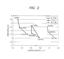
- the band gap can be widened continuously to allow matching of the band offset with the conduction band of Cu(In, Ga)Se 2 in a wide range by the addition of GeO 2 at a band gap of 6 eV and having an identical rutile type crystal structure or ZrO 2 at a band gap of 5 eV or HfO 2 at a band gap 5.5 eV and having a similar fluorite type crystal structure.
- Fig. 10 plots relations between the concentration of the additive materials and the band gap of the buffer layer.
- BaTiO 3 , SrTiO 3 , CaTiO 3 , MgTiO 3 , K(Ta, Nb)O 3 , and Na(Ta, Nb)O 3 are also materials of a perovskite structure having a band gap of 3.2 to 4.4 eV and can control the composition without changing the crystal structure and can control the band gap continuously.
- TiO 2 as the base material and add a BaTiO 3 type or K(Ta, Nb)O 3 type material so long as the range of the concentration for the additive is within a range of solid solution.
- Ti or Ta as main constituent of the base material as the buffer layer material is a higher heat resistant and less diffusing compared with Cd or Zn, and can be used for solid phase selenization of performing annealing after forming the buffer layer.
- Fig. 11 shows the change of the band gap as measured from spectral transmittance upon addition of ZrO 2 to TiO 2 .
- the band gap can be controlled in a range more than 3.6 eV and lower than 3.96 eV and it can be seen that the plotting in Fig. 10 is substantially reproduced.
- Fig. 12 shows a schematic view of a band structure between a TiO 2 type buffer layer and a Cu(In, Ga)Se 2 type absorption layer.
- the band offset ⁇ Ec of the conduction band between the buffer layer and the Cu(In, Ga)Se 2 can be determined by subtracting the sum for the band offset ⁇ Ev of the valence band determined by X-ray photoelectron spectrometry (XPS) and the band gap Eg of the Cu(In, Ga)Se 2 type absorption layer (CIGS) determined by the concentration of additive such as Ga from the band gap Eg (buffer) of the buffer layer determined by a spectrophotometer, etc. shown in Fig. 11 .
- the band gap Eg of the CuInSe 2 absorption layer (CIGS) with no addition of Ga is about 1 eV
- ⁇ Ec can be reduced substantially to 0 eV to allow matching.
- the band gap of Cu(In 0 . 8 , Ga 0 . 2 )Se 2 at 1.2 eV can be reduced to about 0 eV to allow matching by controlling the addition amount of ZrO 2 to 30 at%.
- ⁇ Ec can be matched to 0 eV or more and 0.4 eV or less by controlling the addition amount of ZrO 2 to 40 at% or higher and 85 at% or less.
- ⁇ Ec can be matched to 0 eV or more and 0.4 eV or less to the band gap of the adsorption layer of 1.0 eV or more and 1.75 eV or less by defining the addition amount to 10 at% or more and 65 at% or less in a case of HfO 2 and 10 at% or more and 50 at% or less in a case of GeO 2 .
- the annealing process for crystallization can be carried out by previously depositing them as a cap on Cu(In, Ga)Se 2 precursor film upon solid phase selenization while capping Cu(In, Ga)Se 2 as described above.
- the annealing temperature is restricted to about 400°C for preventing excess diffusion of Zn, crystallization of Cu(In, Ga)Se 2 tends to be insufficient, whereas annealing at 500 to 550°C is possible to crystallize Cu(In, Ga)S e 2 sufficiently in a case of using the embodiment of the invention.
- Fig. 13 shows a result of measuring, by SIMS, (secondary ion mass spectroscopy) the concentration of Zn, Ti, and Mg in Cu(In, Ga)Se 2 prepared by solid phase selenization by using the ZnO type base material (with addition of MgO) and TiO 2 type base material (with addition of MgTiO 3 ) as the buffer layer 4 as the cap. While Zn diffuses at a high concentration of 5 ⁇ 10 19 to 1 ⁇ 10 20 atoms/cm 3 in Cu(In, Ga) Se 2 by annealing at 400°C or higher, Ti and Mg are scarcely diffused and remain below the sensitivity limit of SIMS (10 15 atoms/cm 3 ).
- Cu(In, Ga)Se 2 is doped excessively to the n-type and it is difficult to form a good pn junction.
- a good pn heterojunction or a shallow pn homojunction where Mg is slightly diffused into Cu(In, Ga)Se 2 can be formed for a material using TiO 2 as the base material and using MgTiO 3 as the additive even when high temperature annealing is carried out in solid phase selenization.
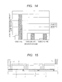
- Fig. 14 shows X-ray diffraction peak intensities of Cu(In, Ga) Se 2 crystals annealed at 400°C and 550°C. It can be seen that Cu(In, Ga) Se 2 crystals annealed at 550°C show strong X-ray diffraction peak intensity and high crystallinity.
- bivalent alkaline earth metals are substitution elements for Cu in Cu(In, Ga)Se 2 and can form a pn homojunction in Cu(In, Ga)Se 2 .
- MnTiO 3 are an optimal substitution material and can form a good homojunction.
- Na in Na (Ta, Nb)O 3 has an effect of enhancing the crystallinity of Cu(In, Ga)Se 2 by diffusion (Na effect).
- the buffer layer 4 and the absorption layer 3 are fabricated each into a rectangular shape on the Mo back electrode 2 by mechanical scribing. Since the absorption layer 3 comprises a material softer than MO, the absorption layer 3 and the buffer layer 4 can be fabricated without damaging the underlying Mo back electrode 2 by properly keeping the fabrication pressure upon mechanical scribing.
- a transparent electrode 5 is formed by a sputtering method.
- the transparent electrode 5 AZO, GZO, and BZO each comprising ZnO and with addition of Al, Ga, and B, respectively can be used for instance.
- the transparent electrode 5, the buffer layer 4, and the absorption layer 3 are fabricated by mechanical scribing. By the step, compound thin film solar cells in serial connection can be formed.
- a substrate type compound thin film solar cell module can be formed by sealing with a cover glass 8 and a back sheet 9 by way of a sealing resin 7 such as EVA (Ethylene Vinyl Acetate) as shown in Fig. 5 .
- EVA Ethylene Vinyl Acetate
- the embodiment of the invention it is possible to provide a material for the buffer layer with no toxicity, having a large wide band gap of 3 eV or more, capable of controlling the band gap width and matching for the band offset of the conduction band with the absorption layer 3, and having good insulation property and high transmittance to the solar spectrum.
- the buffer layer has to be deposited by using the CBD method at low temperature after annealing in hydrogenated Se of high toxicity (gas phase selenization), and this results in a problem in view of the cost for ensuring the safety of the annealing apparatus for gas phase selenization and lowering of the throughput upon mass production due to the combined use of the dry process such as sputtering deposition and the wet process of the CBD method.
- deposition is always carried out by sputtering, and it is possible to use the process of solid phase selenization that does not require annealing in highly toxic hydrogenated Se, thereby enabling to simplify the process and reduce the cost.
- a method of preparing a superstrate type compound thin film solar cell module as a second embodiment of the invention is to be described specifically with reference to the structural view of Fig. 15 and the process flow charts of Figs. 16A and 16B .
- white semi-tempered glass usually used for cover glass is used as a glass substrate 1.
- a transparent electrode film 5 is formed by a sputtering method.
- the transparent electrode 5 for example, AZO, GZO, or BZO each comprising ZnO and with addition of Al, Ga, or B respectively, ITO, IZO, or FTO or ATO each comprising SnO 2 with addition of F or Sb, respectively, can be used.
- the film of the transparent electrode 5 is fabricated into a rectangular shape by using laser scribing or the like.
- the fabrication pitch is about 3 to 10 mm, the number of rectangles is designed in accordance with the design for the size of the glass substrate 1, the output voltage, and the electrode resistance, and the fabrication width is decided.
- the n-type buffer layer 4 uses a material, for example, comprising TiO 2 as a base material with addition of ZrO 2 , HfO 2 , GeO 2 , etc. for band gap control, BaTiO 3 as a base material with addition of SrTiO 3 , CaTiO 3 , or MgTiO 3 for band gap control, K(Ta, Nb)O 3 as a base material with addition of Na(Ta, Nb)O 3 for band gap control, or TiO 2 as a base material in combination with one or plurality of BaTiO 3 type, K(Ti, Nb)O 3 type materials as the additive.
- TiO 2 as a base material with addition of ZrO 2 , HfO 2 , GeO 2 , etc.
- BaTiO 3 as a base material with addition of SrTiO 3 , CaTiO 3 , or MgTiO 3 for band gap control
- K(Ta, Nb)O 3 as a
- the precursor film for the absorption layer 3 is also formed by the sputtering method.
- the film thickness is from 1 to 3 ⁇ m.
- the Cu(In, Ga)Se 2 type absorption layer 3 is formed by gas phase selenization, a multilayer film of a Cu-Ga alloy and In is deposited and, subsequently, annealed in a hydrogenated Se gas atmosphere at a temperature of about 500 to 550°C as shown in Fig. 16A , to form an adsorption layer.
- solid phase selenization can also be used by also depositing Se together with a metal film by sputtering and then annealing them.
- the precursor film of the absorption layer 3 and the buffer layer 4 are fabricated by mechanical scribing, etc., then Mo is deposited as the back electrode 2 and annealing is carried out for crystallization in an inert gas while capping by Mo. Since each of the materials of the buffer layer 4 of the invention has higher heat resistance compared with CdS or ZnO, and does not diffuse excessively during the annealing process for crystallization as described above, it is possible to make the annealing temperature sufficiently high and the crystallinity of Cu(In, Ga)Se 2 can be enhanced. Further, it is also possible to protect the transparent electrode 5 and prevent increase of the resistivity of the transparent electrode.
- the cell structure is a superstrate structure in which the glass substrate 1 is on the light incident side, modulation is attained by merely bonding the glass substrate 1 and the back sheet 9 by way of the EVA sheet 7 to each other as shown in Fig. 6 without requiring the cover glass 8. Accordingly, it is possible to save the number of parts and reduce the cost compared with the existent Cu (In, Ga)Se 2 compound thin film solar cell module.
- n-type TiO 2 Control of the band gap by adding other oxides to the base material of n-type TiO 2 has been disclosed above.
- the n-type oxide semiconductor such as TiO 2 shows an n-type semiconductor property due to slight deficiency of oxygen in the crystals.
- n-type TiO 2 can be deposited by sputtering deposition in an Ar atmosphere. In the first embodiment or the second embodiment, sputtering deposition has been performed in a pure Ar atmosphere with no addition of oxygen.
- Fig. 17 shows a current-voltage curve 12 in a buffer layer using TiO 2 prepared under such a condition.
- the present inventor has experimentally found that a further larger photogenerated current can be obtained not relying on oxygen deficiency but providing TiO 2 with electroconductivity by substituting 4-valent Ti with 5-valent element.
- the current-voltage curve 13 in Fig. 17 in a case of doping Nb by 10% to a buffer layer using TiO 2 shows a power generation property when Nb is doped by 10% to TiO 2 thereby obtaining n-conduction type.
- the conduction band offset ⁇ Ec is lowered by addition of Nb and the photogenerated current can take a further larger value to improve the power generation property.
- the band gap of the CIGS semiconductor in this case is 1.06 eV.
- the addition amount of Nb is to be referred to.
- Nb is doped at a high concentration to TiO 2 to form a degenerate semiconductor in a metal state, this transfers from a semiconductor hetero-junction to a metal-semiconductor junction.
- the conduction band offset is estimated as -0.25 eV. That is, the conduction band offset shows +0.6 eV when TiO 2 is in the state of an insulator and shows -0.25 eV when it is a degenerate semiconductor in the state of metal.
- ⁇ Ec takes a value of -0.25 eV or more and +0.6 eV or less.
- the upper limit of the carrier concentration is preferably in a range not causing degeneration.
- the carrier concentration is preferably 10 18 cm -3 or less.
- the thickness of the buffer layer may be controlled generally in accordance with the carrier concentration, that is, the thickness may be larger when the carrier concentration is higher and smaller when the concentration is lower. Specifically, the thickness may be controlled such that the conversion efficiency is at the maximum level within a range of 10 nm or more and 300 nm or less.
- Nb has been used as the dopant to TiO 2 in this case, the same effect can be expected also by using other element belonging to the group VA of the periodical table such as vanadium V or tantalum Ta.
- the carrier concentration is preferably 10 15 cm -3 or more and 10 19 cm -3 or less in the same manner.
- Nb having an ionic radius close to that of Ti is most preferred since the electric activity is high.
- the invention is effective when applied to the Cu(In, Ga)Se 2 type compound thin film solar cell and module and can be utilized generally in the industrial field of power generation solar cell for the use of residential houses and mega-solar facilities.
Landscapes
- Photovoltaic Devices (AREA)
Applications Claiming Priority (2)
| Application Number | Priority Date | Filing Date | Title |
|---|---|---|---|
| JP2009296692 | 2009-12-28 | ||
| JP2010135673A JP2011155237A (ja) | 2009-12-28 | 2010-06-15 | 化合物薄膜太陽電池、化合物薄膜太陽電池の製造方法、および化合物薄膜太陽電池モジュール |
Publications (1)
| Publication Number | Publication Date |
|---|---|
| EP2339641A2 true EP2339641A2 (fr) | 2011-06-29 |
Family
ID=43982288
Family Applications (1)
| Application Number | Title | Priority Date | Filing Date |
|---|---|---|---|
| EP10172010A Withdrawn EP2339641A2 (fr) | 2009-12-28 | 2010-08-05 | Cellule solaire à film mince à semiconducteur composé, procédé de fabrication d'une cellule solaire et panneau solaire à film mince à semiconducteur composé |
Country Status (4)
| Country | Link |
|---|---|
| US (1) | US20110155226A1 (fr) |
| EP (1) | EP2339641A2 (fr) |
| JP (1) | JP2011155237A (fr) |
| CN (1) | CN102110722A (fr) |
Cited By (10)
| Publication number | Priority date | Publication date | Assignee | Title |
|---|---|---|---|---|
| WO2014188386A1 (fr) | 2013-05-24 | 2014-11-27 | Commissariat A L'energie Atomique Et Aux Energies Alternatives | PROCEDE DE REALISATION DE LA JONCTION p-n D'UNE CELLULE PHOTOVOLTAIQUE EN COUCHES MINCES ET PROCEDE D'OBTENTION CORRESPONDANT D'UNE CELLULE PHOTOVOLTAÏQUE. |
| EP3007236A4 (fr) * | 2013-06-05 | 2017-01-18 | Jun, Young-kwon | Cellule solaire et procédé de fabrication de ladite cellule |
| US9786807B2 (en) | 2011-04-19 | 2017-10-10 | Empa | Thin-film photovoltaic device and fabrication method |
| US9837565B2 (en) | 2012-12-21 | 2017-12-05 | Flison Ag | Fabricating thin-film optoelectronic devices with added potassium |
| WO2018191358A1 (fr) * | 2017-04-14 | 2018-10-18 | Hee Solar, L.L.C. | Encapsulation de dispositif photovoltaïque |
| US10109761B2 (en) | 2014-05-23 | 2018-10-23 | Flisom Ag | Fabricating thin-film optoelectronic devices with modified surface |
| US10396218B2 (en) | 2014-09-18 | 2019-08-27 | Flisom Ag | Self-assembly pattering for fabricating thin-film devices |
| US10651324B2 (en) | 2016-02-11 | 2020-05-12 | Flisom Ag | Self-assembly patterning for fabricating thin-film devices |
| US10658532B2 (en) | 2016-02-11 | 2020-05-19 | Flisom Ag | Fabricating thin-film optoelectronic devices with added rubidium and/or cesium |
| CN113178506A (zh) * | 2021-04-22 | 2021-07-27 | 中国海洋大学 | 基于过渡金属硫化物/三元硫化物量子点复合空穴传输层的钙钛矿太阳能电池及制备方法 |
Families Citing this family (21)
| Publication number | Priority date | Publication date | Assignee | Title |
|---|---|---|---|---|
| US8617915B2 (en) * | 2010-09-20 | 2013-12-31 | International Business Machines Corporation | Annealing thin films |
| US8530263B2 (en) * | 2011-08-10 | 2013-09-10 | Taiwan Semiconductor Manufacturing Co., Ltd. | Superstrate solar cell |
| KR101283078B1 (ko) * | 2011-11-07 | 2013-07-05 | 엘지이노텍 주식회사 | 태양광 발전장치 및 이의 제조방법 |
| JP2013125832A (ja) * | 2011-12-14 | 2013-06-24 | Toyota Motor Corp | ZnO系膜及びその製造方法 |
| CN104364910B (zh) * | 2012-01-31 | 2016-12-21 | 陶氏环球技术有限责任公司 | 制造磷属元素化物吸收体膜和发射体膜之间导带偏移降低的光伏器件的方法 |
| US9390917B2 (en) | 2012-02-21 | 2016-07-12 | Zetta Research and Development LLC—AQT Series | Closed-space sublimation process for production of CZTS thin-films |
| KR101849267B1 (ko) | 2012-07-06 | 2018-04-17 | 한국전자통신연구원 | 박막 태양전지 및 그의 제조 방법 |
| JP5783984B2 (ja) * | 2012-09-26 | 2015-09-24 | 株式会社東芝 | 光電変換素子と太陽電池及びこれらの製造方法 |
| CN103050554B (zh) * | 2012-12-07 | 2015-04-01 | 上海交通大学 | 太阳能集热发电一体化薄膜及其构成的发电集热热水器 |
| KR20140146998A (ko) * | 2013-06-17 | 2014-12-29 | 전영권 | 태양전지 및 그 제조방법 |
| JP5667714B1 (ja) * | 2014-06-16 | 2015-02-12 | 積水化学工業株式会社 | 薄膜太陽電池及び薄膜太陽電池の製造方法 |
| JP5667715B1 (ja) * | 2014-06-16 | 2015-02-12 | 積水化学工業株式会社 | 薄膜太陽電池及び薄膜太陽電池の製造方法 |
| US9466755B2 (en) | 2014-10-30 | 2016-10-11 | International Business Machines Corporation | MIS-IL silicon solar cell with passivation layer to induce surface inversion |
| US10121920B2 (en) * | 2015-06-30 | 2018-11-06 | International Business Machines Corporation | Aluminum-doped zinc oxysulfide emitters for enhancing efficiency of chalcogenide solar cell |
| JP6955915B2 (ja) * | 2016-08-03 | 2021-10-27 | パナソニック株式会社 | 太陽電池モジュールおよびその製造方法 |
| CN107123693B (zh) * | 2017-04-14 | 2020-05-22 | 华南理工大学 | 一种基于溶液法加工的具有高透明窗口层材料的高效CdTe纳米晶太阳电池及其制备方法 |
| CN114424348B (zh) | 2019-07-25 | 2024-04-26 | 中国建材国际工程集团有限公司 | 用于产生双梯度CdSeTe薄膜结构的方法 |
| CN112259686B (zh) * | 2020-10-09 | 2023-12-29 | 隆基绿能科技股份有限公司 | 一种叠层电池及其制作方法 |
| CN112490309B (zh) * | 2020-12-07 | 2022-10-25 | 中国科学院长春光学精密机械与物理研究所 | 一种薄膜紫外探测器及其制备方法 |
| CN113209290B (zh) * | 2021-04-12 | 2022-03-29 | 华南理工大学 | 一种增强声动力抗肿瘤的铋/钛酸钡异质结及其制备方法 |
| KR102849564B1 (ko) * | 2023-11-23 | 2025-08-25 | 한국과학기술연구원 | 양면수광형 박막태양전지 및 그 제조방법 |
Citations (2)
| Publication number | Priority date | Publication date | Assignee | Title |
|---|---|---|---|---|
| US4611091A (en) | 1984-12-06 | 1986-09-09 | Atlantic Richfield Company | CuInSe2 thin film solar cell with thin CdS and transparent window layer |
| JP2006147759A (ja) | 2004-11-18 | 2006-06-08 | Honda Motor Co Ltd | カルコパイライト型薄膜太陽電池の製造方法 |
Family Cites Families (3)
| Publication number | Priority date | Publication date | Assignee | Title |
|---|---|---|---|---|
| JP2004079610A (ja) * | 2002-08-12 | 2004-03-11 | Masaharu Kaneko | TiO2薄膜及び色素増感太陽電池用電極の作製方法並びに色素増感太陽電池用電極 |
| JP4969785B2 (ja) * | 2005-02-16 | 2012-07-04 | 本田技研工業株式会社 | カルコパイライト型太陽電池及びその製造方法 |
| JP2007324633A (ja) * | 2007-09-14 | 2007-12-13 | Masayoshi Murata | 集積化タンデム型薄膜シリコン太陽電池モジュール及びその製造方法 |
-
2010
- 2010-06-15 JP JP2010135673A patent/JP2011155237A/ja active Pending
- 2010-08-05 EP EP10172010A patent/EP2339641A2/fr not_active Withdrawn
- 2010-08-13 US US12/855,763 patent/US20110155226A1/en not_active Abandoned
- 2010-08-13 CN CN2010102544219A patent/CN102110722A/zh active Pending
Patent Citations (2)
| Publication number | Priority date | Publication date | Assignee | Title |
|---|---|---|---|---|
| US4611091A (en) | 1984-12-06 | 1986-09-09 | Atlantic Richfield Company | CuInSe2 thin film solar cell with thin CdS and transparent window layer |
| JP2006147759A (ja) | 2004-11-18 | 2006-06-08 | Honda Motor Co Ltd | カルコパイライト型薄膜太陽電池の製造方法 |
Non-Patent Citations (1)
| Title |
|---|
| "Recent development of thin film compound semiconductor photovoltaic cells", CMC, 30 June 2007 (2007-06-30), pages 81 |
Cited By (17)
| Publication number | Priority date | Publication date | Assignee | Title |
|---|---|---|---|---|
| US9786807B2 (en) | 2011-04-19 | 2017-10-10 | Empa | Thin-film photovoltaic device and fabrication method |
| US9837565B2 (en) | 2012-12-21 | 2017-12-05 | Flison Ag | Fabricating thin-film optoelectronic devices with added potassium |
| US10153387B2 (en) | 2012-12-21 | 2018-12-11 | Flisom Ag | Fabricating thin-film optoelectronic devices with added potassium |
| WO2014188386A1 (fr) | 2013-05-24 | 2014-11-27 | Commissariat A L'energie Atomique Et Aux Energies Alternatives | PROCEDE DE REALISATION DE LA JONCTION p-n D'UNE CELLULE PHOTOVOLTAIQUE EN COUCHES MINCES ET PROCEDE D'OBTENTION CORRESPONDANT D'UNE CELLULE PHOTOVOLTAÏQUE. |
| EP3007236A4 (fr) * | 2013-06-05 | 2017-01-18 | Jun, Young-kwon | Cellule solaire et procédé de fabrication de ladite cellule |
| US10672941B2 (en) | 2014-05-23 | 2020-06-02 | Flisom Ag | Fabricating thin-film optoelectronic devices with modified surface |
| US10109761B2 (en) | 2014-05-23 | 2018-10-23 | Flisom Ag | Fabricating thin-film optoelectronic devices with modified surface |
| US10431709B2 (en) | 2014-05-23 | 2019-10-01 | Flisom Ag | Fabricating thin-film optoelectronic devices with modified surface |
| US10396218B2 (en) | 2014-09-18 | 2019-08-27 | Flisom Ag | Self-assembly pattering for fabricating thin-film devices |
| US10971640B2 (en) | 2016-02-11 | 2021-04-06 | Flisom Ag | Self-assembly patterning for fabricating thin-film devices |
| US10658532B2 (en) | 2016-02-11 | 2020-05-19 | Flisom Ag | Fabricating thin-film optoelectronic devices with added rubidium and/or cesium |
| US10651324B2 (en) | 2016-02-11 | 2020-05-12 | Flisom Ag | Self-assembly patterning for fabricating thin-film devices |
| US11257966B2 (en) | 2016-02-11 | 2022-02-22 | Flisom Ag | Fabricating thin-film optoelectronic devices with added rubidium and/or cesium |
| WO2018191358A1 (fr) * | 2017-04-14 | 2018-10-18 | Hee Solar, L.L.C. | Encapsulation de dispositif photovoltaïque |
| US12046425B2 (en) | 2017-04-14 | 2024-07-23 | Cubicpv Inc. | Photovoltaic device encapsulation |
| CN113178506A (zh) * | 2021-04-22 | 2021-07-27 | 中国海洋大学 | 基于过渡金属硫化物/三元硫化物量子点复合空穴传输层的钙钛矿太阳能电池及制备方法 |
| CN113178506B (zh) * | 2021-04-22 | 2022-02-11 | 中国海洋大学 | 基于过渡金属硫化物/三元硫化物量子点复合空穴传输层的钙钛矿太阳能电池及制备方法 |
Also Published As
| Publication number | Publication date |
|---|---|
| CN102110722A (zh) | 2011-06-29 |
| JP2011155237A (ja) | 2011-08-11 |
| US20110155226A1 (en) | 2011-06-30 |
Similar Documents
| Publication | Publication Date | Title |
|---|---|---|
| EP2339641A2 (fr) | Cellule solaire à film mince à semiconducteur composé, procédé de fabrication d'une cellule solaire et panneau solaire à film mince à semiconducteur composé | |
| KR101503557B1 (ko) | 계면 층을 포함한 광기전 장치 | |
| US11908970B2 (en) | Process for manufacturing multilayered thin film, method of manufacturing solar cell, and method for manufacturing solar cell module | |
| US20120204939A1 (en) | Structure and Method for High Efficiency CIS/CIGS-based Tandem Photovoltaic Module | |
| EP2309548A2 (fr) | Dispositif de conversion photoélectrique, son procédé de fabrication et batterie solaire | |
| US20140076392A1 (en) | Solar cell | |
| JP7503777B1 (ja) | 太陽電池の製造方法及び太陽電池 | |
| JP2014209586A (ja) | 薄膜太陽電池及びその製造方法 | |
| US20250359349A1 (en) | Solar cell, method for manufacturing solar cell, multi-junction solar cell, solar cell module, and photovoltaic power generation system | |
| JP6147926B2 (ja) | ナトリウムインジウム硫化物緩衝層を有する薄膜太陽電池のための層システム | |
| WO2025094603A1 (fr) | Procédé de fabrication de cellule solaire et cellule solaire | |
| EP2787537B1 (fr) | CELLULE SOLAIRE EN COUCHES MINCES avec couche tampon à sulfure d'indium | |
| KR101300642B1 (ko) | 태양전지 | |
| CN103348488B (zh) | 具有金属硫氧化物窗口层的光伏装置 | |
| US20130247994A1 (en) | Photovoltaic device | |
| JP2012532446A (ja) | 太陽電池及びその製造方法 | |
| US20140261689A1 (en) | Method of manufacturing a photovoltaic device | |
| LU504697B1 (en) | Thin film solar cell and corresponding production method | |
| JP7457311B1 (ja) | 太陽電池及び太陽電池の製造方法 | |
| JP7747360B1 (ja) | 太陽電池及び太陽電池の製造方法 | |
| WO2025158960A1 (fr) | Procédé permettant de fabriquer une cellule solaire et cellule solaire | |
| JP5842991B2 (ja) | 化合物半導体太陽電池 | |
| JP2014127580A (ja) | 光電変換装置の製造方法 |
Legal Events
| Date | Code | Title | Description |
|---|---|---|---|
| PUAI | Public reference made under article 153(3) epc to a published international application that has entered the european phase |
Free format text: ORIGINAL CODE: 0009012 |
|
| 17P | Request for examination filed |
Effective date: 20101130 |
|
| AK | Designated contracting states |
Kind code of ref document: A2 Designated state(s): AL AT BE BG CH CY CZ DE DK EE ES FI FR GB GR HR HU IE IS IT LI LT LU LV MC MK MT NL NO PL PT RO SE SI SK SM TR |
|
| AX | Request for extension of the european patent |
Extension state: BA ME RS |
|
| STAA | Information on the status of an ep patent application or granted ep patent |
Free format text: STATUS: THE APPLICATION IS DEEMED TO BE WITHDRAWN |
|
| 18D | Application deemed to be withdrawn |
Effective date: 20130301 |