EP2339643A2 - Photovoltaikzelle - Google Patents
Photovoltaikzelle Download PDFInfo
- Publication number
- EP2339643A2 EP2339643A2 EP20100196024 EP10196024A EP2339643A2 EP 2339643 A2 EP2339643 A2 EP 2339643A2 EP 20100196024 EP20100196024 EP 20100196024 EP 10196024 A EP10196024 A EP 10196024A EP 2339643 A2 EP2339643 A2 EP 2339643A2
- Authority
- EP
- European Patent Office
- Prior art keywords
- cell
- type
- photo
- cdte
- layer
- Prior art date
- Legal status (The legal status is an assumption and is not a legal conclusion. Google has not performed a legal analysis and makes no representation as to the accuracy of the status listed.)
- Withdrawn
Links
- 239000006096 absorbing agent Substances 0.000 claims abstract description 65
- 239000004065 semiconductor Substances 0.000 claims abstract description 40
- 150000001875 compounds Chemical class 0.000 claims abstract description 9
- MARUHZGHZWCEQU-UHFFFAOYSA-N 5-phenyl-2h-tetrazole Chemical compound C1=CC=CC=C1C1=NNN=N1 MARUHZGHZWCEQU-UHFFFAOYSA-N 0.000 claims description 88
- 239000000463 material Substances 0.000 claims description 35
- CJOBVZJTOIVNNF-UHFFFAOYSA-N cadmium sulfide Chemical compound [Cd]=S CJOBVZJTOIVNNF-UHFFFAOYSA-N 0.000 claims description 13
- 229910052980 cadmium sulfide Inorganic materials 0.000 claims description 13
- XLOMVQKBTHCTTD-UHFFFAOYSA-N Zinc monoxide Chemical compound [Zn]=O XLOMVQKBTHCTTD-UHFFFAOYSA-N 0.000 claims description 11
- 239000011787 zinc oxide Substances 0.000 claims description 7
- 239000011248 coating agent Substances 0.000 claims description 6
- 238000000576 coating method Methods 0.000 claims description 6
- 239000002070 nanowire Substances 0.000 claims description 6
- 239000002096 quantum dot Substances 0.000 claims description 5
- XOLBLPGZBRYERU-UHFFFAOYSA-N tin dioxide Chemical compound O=[Sn]=O XOLBLPGZBRYERU-UHFFFAOYSA-N 0.000 claims description 5
- JAONJTDQXUSBGG-UHFFFAOYSA-N dialuminum;dizinc;oxygen(2-) Chemical compound [O-2].[O-2].[O-2].[O-2].[O-2].[Al+3].[Al+3].[Zn+2].[Zn+2] JAONJTDQXUSBGG-UHFFFAOYSA-N 0.000 claims description 4
- 229910003437 indium oxide Inorganic materials 0.000 claims description 4
- PJXISJQVUVHSOJ-UHFFFAOYSA-N indium(iii) oxide Chemical compound [O-2].[O-2].[O-2].[In+3].[In+3] PJXISJQVUVHSOJ-UHFFFAOYSA-N 0.000 claims description 4
- 239000002071 nanotube Substances 0.000 claims description 4
- 229910052793 cadmium Inorganic materials 0.000 claims description 3
- BEQNOZDXPONEMR-UHFFFAOYSA-N cadmium;oxotin Chemical compound [Cd].[Sn]=O BEQNOZDXPONEMR-UHFFFAOYSA-N 0.000 claims description 3
- AMGQUBHHOARCQH-UHFFFAOYSA-N indium;oxotin Chemical compound [In].[Sn]=O AMGQUBHHOARCQH-UHFFFAOYSA-N 0.000 claims description 3
- 229940071182 stannate Drugs 0.000 claims description 3
- 229910001887 tin oxide Inorganic materials 0.000 claims description 3
- QHGNHLZPVBIIPX-UHFFFAOYSA-N tin(ii) oxide Chemical class [Sn]=O QHGNHLZPVBIIPX-UHFFFAOYSA-N 0.000 claims description 3
- YVTHLONGBIQYBO-UHFFFAOYSA-N zinc indium(3+) oxygen(2-) Chemical compound [O--].[Zn++].[In+3] YVTHLONGBIQYBO-UHFFFAOYSA-N 0.000 claims description 3
- 230000003287 optical effect Effects 0.000 description 17
- 238000013461 design Methods 0.000 description 15
- 230000004907 flux Effects 0.000 description 14
- 239000000758 substrate Substances 0.000 description 14
- 230000005684 electric field Effects 0.000 description 11
- 239000011669 selenium Substances 0.000 description 9
- 238000006243 chemical reaction Methods 0.000 description 8
- 238000009434 installation Methods 0.000 description 8
- 229910052711 selenium Inorganic materials 0.000 description 7
- 239000002800 charge carrier Substances 0.000 description 5
- 239000010949 copper Substances 0.000 description 5
- 238000011161 development Methods 0.000 description 5
- BUGBHKTXTAQXES-UHFFFAOYSA-N Selenium Chemical compound [Se] BUGBHKTXTAQXES-UHFFFAOYSA-N 0.000 description 4
- NINIDFKCEFEMDL-UHFFFAOYSA-N Sulfur Chemical compound [S] NINIDFKCEFEMDL-UHFFFAOYSA-N 0.000 description 4
- 239000005864 Sulphur Substances 0.000 description 4
- 230000009471 action Effects 0.000 description 4
- 230000005611 electricity Effects 0.000 description 4
- 238000001228 spectrum Methods 0.000 description 4
- 229910052714 tellurium Inorganic materials 0.000 description 4
- PORWMNRCUJJQNO-UHFFFAOYSA-N tellurium atom Chemical compound [Te] PORWMNRCUJJQNO-UHFFFAOYSA-N 0.000 description 4
- SKJCKYVIQGBWTN-UHFFFAOYSA-N (4-hydroxyphenyl) methanesulfonate Chemical compound CS(=O)(=O)OC1=CC=C(O)C=C1 SKJCKYVIQGBWTN-UHFFFAOYSA-N 0.000 description 3
- PFNQVRZLDWYSCW-UHFFFAOYSA-N (fluoren-9-ylideneamino) n-naphthalen-1-ylcarbamate Chemical compound C12=CC=CC=C2C2=CC=CC=C2C1=NOC(=O)NC1=CC=CC2=CC=CC=C12 PFNQVRZLDWYSCW-UHFFFAOYSA-N 0.000 description 3
- JBRZTFJDHDCESZ-UHFFFAOYSA-N AsGa Chemical compound [As]#[Ga] JBRZTFJDHDCESZ-UHFFFAOYSA-N 0.000 description 3
- 229910001218 Gallium arsenide Inorganic materials 0.000 description 3
- 229910000530 Gallium indium arsenide Inorganic materials 0.000 description 3
- 239000005083 Zinc sulfide Substances 0.000 description 3
- KTSFMFGEAAANTF-UHFFFAOYSA-N [Cu].[Se].[Se].[In] Chemical compound [Cu].[Se].[Se].[In] KTSFMFGEAAANTF-UHFFFAOYSA-N 0.000 description 3
- KXNLCSXBJCPWGL-UHFFFAOYSA-N [Ga].[As].[In] Chemical compound [Ga].[As].[In] KXNLCSXBJCPWGL-UHFFFAOYSA-N 0.000 description 3
- 239000011149 active material Substances 0.000 description 3
- 229910052782 aluminium Inorganic materials 0.000 description 3
- WILFBXOGIULNAF-UHFFFAOYSA-N copper sulfanylidenetin zinc Chemical compound [Sn]=S.[Zn].[Cu] WILFBXOGIULNAF-UHFFFAOYSA-N 0.000 description 3
- 230000007547 defect Effects 0.000 description 3
- 229910052733 gallium Inorganic materials 0.000 description 3
- AKUCEXGLFUSJCD-UHFFFAOYSA-N indium(3+);selenium(2-) Chemical compound [Se-2].[Se-2].[Se-2].[In+3].[In+3] AKUCEXGLFUSJCD-UHFFFAOYSA-N 0.000 description 3
- SIXIBASSFIFHDK-UHFFFAOYSA-N indium(3+);trisulfide Chemical compound [S-2].[S-2].[S-2].[In+3].[In+3] SIXIBASSFIFHDK-UHFFFAOYSA-N 0.000 description 3
- 238000000034 method Methods 0.000 description 3
- 230000000704 physical effect Effects 0.000 description 3
- 229910052709 silver Inorganic materials 0.000 description 3
- GPXJNWSHGFTCBW-UHFFFAOYSA-N Indium phosphide Chemical compound [In]#P GPXJNWSHGFTCBW-UHFFFAOYSA-N 0.000 description 2
- 229910052779 Neodymium Inorganic materials 0.000 description 2
- 229910052777 Praseodymium Inorganic materials 0.000 description 2
- HCHKCACWOHOZIP-UHFFFAOYSA-N Zinc Chemical compound [Zn] HCHKCACWOHOZIP-UHFFFAOYSA-N 0.000 description 2
- 238000013459 approach Methods 0.000 description 2
- 238000004891 communication Methods 0.000 description 2
- LCUOIYYHNRBAFS-UHFFFAOYSA-N copper;sulfanylideneindium Chemical compound [Cu].[In]=S LCUOIYYHNRBAFS-UHFFFAOYSA-N 0.000 description 2
- 230000000694 effects Effects 0.000 description 2
- 230000006872 improvement Effects 0.000 description 2
- 229910052747 lanthanoid Inorganic materials 0.000 description 2
- 150000002602 lanthanoids Chemical class 0.000 description 2
- 238000004519 manufacturing process Methods 0.000 description 2
- VNWKTOKETHGBQD-UHFFFAOYSA-N methane Chemical compound C VNWKTOKETHGBQD-UHFFFAOYSA-N 0.000 description 2
- QEFYFXOXNSNQGX-UHFFFAOYSA-N neodymium atom Chemical compound [Nd] QEFYFXOXNSNQGX-UHFFFAOYSA-N 0.000 description 2
- PUDIUYLPXJFUGB-UHFFFAOYSA-N praseodymium atom Chemical compound [Pr] PUDIUYLPXJFUGB-UHFFFAOYSA-N 0.000 description 2
- 230000008569 process Effects 0.000 description 2
- 239000010409 thin film Substances 0.000 description 2
- 229910052725 zinc Inorganic materials 0.000 description 2
- 239000011701 zinc Substances 0.000 description 2
- DRDVZXDWVBGGMH-UHFFFAOYSA-N zinc;sulfide Chemical compound [S-2].[Zn+2] DRDVZXDWVBGGMH-UHFFFAOYSA-N 0.000 description 2
- 238000010521 absorption reaction Methods 0.000 description 1
- 230000004075 alteration Effects 0.000 description 1
- 230000003190 augmentative effect Effects 0.000 description 1
- AQCDIIAORKRFCD-UHFFFAOYSA-N cadmium selenide Chemical compound [Cd]=[Se] AQCDIIAORKRFCD-UHFFFAOYSA-N 0.000 description 1
- UHYPYGJEEGLRJD-UHFFFAOYSA-N cadmium(2+);selenium(2-) Chemical compound [Se-2].[Cd+2] UHYPYGJEEGLRJD-UHFFFAOYSA-N 0.000 description 1
- 239000003245 coal Substances 0.000 description 1
- 230000007423 decrease Effects 0.000 description 1
- 239000003989 dielectric material Substances 0.000 description 1
- 230000003292 diminished effect Effects 0.000 description 1
- 239000011521 glass Substances 0.000 description 1
- 239000012535 impurity Substances 0.000 description 1
- 239000003345 natural gas Substances 0.000 description 1
- VIKNJXKGJWUCNN-XGXHKTLJSA-N norethisterone Chemical compound O=C1CC[C@@H]2[C@H]3CC[C@](C)([C@](CC4)(O)C#C)[C@@H]4[C@@H]3CCC2=C1 VIKNJXKGJWUCNN-XGXHKTLJSA-N 0.000 description 1
- 238000013082 photovoltaic technology Methods 0.000 description 1
- 239000011148 porous material Substances 0.000 description 1
- -1 quantum wires Substances 0.000 description 1
- 238000012827 research and development Methods 0.000 description 1
- 238000006467 substitution reaction Methods 0.000 description 1
Images

Classifications
-
- H—ELECTRICITY
- H10—SEMICONDUCTOR DEVICES; ELECTRIC SOLID-STATE DEVICES NOT OTHERWISE PROVIDED FOR
- H10F—INORGANIC SEMICONDUCTOR DEVICES SENSITIVE TO INFRARED RADIATION, LIGHT, ELECTROMAGNETIC RADIATION OF SHORTER WAVELENGTH OR CORPUSCULAR RADIATION
- H10F71/00—Manufacture or treatment of devices covered by this subclass
- H10F71/125—The active layers comprising only Group II-VI materials, e.g. CdS, ZnS or CdTe
-
- H—ELECTRICITY
- H10—SEMICONDUCTOR DEVICES; ELECTRIC SOLID-STATE DEVICES NOT OTHERWISE PROVIDED FOR
- H10F—INORGANIC SEMICONDUCTOR DEVICES SENSITIVE TO INFRARED RADIATION, LIGHT, ELECTROMAGNETIC RADIATION OF SHORTER WAVELENGTH OR CORPUSCULAR RADIATION
- H10F77/00—Constructional details of devices covered by this subclass
- H10F77/10—Semiconductor bodies
- H10F77/14—Shape of semiconductor bodies; Shapes, relative sizes or dispositions of semiconductor regions within semiconductor bodies
- H10F77/143—Shape of semiconductor bodies; Shapes, relative sizes or dispositions of semiconductor regions within semiconductor bodies comprising quantum structures
- H10F77/1437—Quantum wires or nanorods
-
- H—ELECTRICITY
- H10—SEMICONDUCTOR DEVICES; ELECTRIC SOLID-STATE DEVICES NOT OTHERWISE PROVIDED FOR
- H10F—INORGANIC SEMICONDUCTOR DEVICES SENSITIVE TO INFRARED RADIATION, LIGHT, ELECTROMAGNETIC RADIATION OF SHORTER WAVELENGTH OR CORPUSCULAR RADIATION
- H10F77/00—Constructional details of devices covered by this subclass
- H10F77/10—Semiconductor bodies
- H10F77/14—Shape of semiconductor bodies; Shapes, relative sizes or dispositions of semiconductor regions within semiconductor bodies
- H10F77/148—Shapes of potential barriers
-
- Y—GENERAL TAGGING OF NEW TECHNOLOGICAL DEVELOPMENTS; GENERAL TAGGING OF CROSS-SECTIONAL TECHNOLOGIES SPANNING OVER SEVERAL SECTIONS OF THE IPC; TECHNICAL SUBJECTS COVERED BY FORMER USPC CROSS-REFERENCE ART COLLECTIONS [XRACs] AND DIGESTS
- Y02—TECHNOLOGIES OR APPLICATIONS FOR MITIGATION OR ADAPTATION AGAINST CLIMATE CHANGE
- Y02E—REDUCTION OF GREENHOUSE GAS [GHG] EMISSIONS, RELATED TO ENERGY GENERATION, TRANSMISSION OR DISTRIBUTION
- Y02E10/00—Energy generation through renewable energy sources
- Y02E10/50—Photovoltaic [PV] energy
- Y02E10/543—Solar cells from Group II-VI materials
Definitions
- the invention relates generally to the area of semiconductor photovoltaic (PV) cells. More specifically, the invention relates to the area of PV cells wherein the semiconductor absorber material employed is cadmium telluride (CdTe).
- the semiconductor absorber material employed is cadmium telluride (CdTe).
- the solar spectrum "sunlight” contains a distribution of intensity as a function of frequency. It can be shown that the conversion efficiency for utilizing sunlight to obtain electricity via semiconductors is optimized for semiconducting band-gaps that range from about 1.4-1.5 electron volt (eV).
- the semiconducting band-gap of CdTe is a good match for this requirement.
- PV cells including CdTe as the photo-active material may be referred to as "CdTe PV cells.”
- Improvement in the overall efficiency of CdTe PV installations will enhance their competitiveness compared to traditional methods of generating electricity such as from natural gas, or coal. It is evident that improvement in overall efficiency will enable CdTe PV technology to successfully penetrate markets where small-scale area confined installations are required, such as markets for domestic PV installations.
- a CdTe PV cell design that is more reliable and enables conversion efficiencies in excess of the efficiencies of present generation CdTe PV cells, would therefore be highly desirable.
- Embodiments of the invention are directed to a photovoltaic cell.
- a photovoltaic (PV) cell comprising, a plurality of ultrafine structures electrically coupled to, and embedded within, a polycrystalline photo-active absorber layer comprising p-type cadmium telluride (CdTe).
- a photovoltaic solar cell comprising, an optical-window-electrode (OWE) layer, a plurality of ultrafine structures comprising an n-type semiconductor electrically coupled to, and embedded within and substantially along a thickness direction of, a polycrystalline photo-active absorber layer comprising p-type cadmium telluride (CdTe), and a electrode layer comprising a p-type semiconductor.
- OBE optical-window-electrode
- CdTe p-type cadmium telluride
- a photovoltaic (PV) cell comprising, a plurality of ultrafine structures electrically coupled to, and embedded within, a polycrystalline photo-active absorber layer comprising a p-type compound semiconductor.
- embodiments of the invention are directed to improved photovoltaic (PV) cell designs.
- PV photovoltaic
- Particular embodiments of the invention proposed here provide for a PV cell including a photo-active absorber layer including n-type CdTe, and having an efficiency that is enhanced over the efficiencies of presently available CdTe PV cells (about 16.5%).
- Embodiments of the CdTe PV cell disclosed herein may display an efficiency that approaches, or even exceeds, about 20%.
- the photo-active absorber layer disclosed herein is the part of the PV cell where the conversion of electromagnetic energy of incident light, for instance, sunlight, to electrical energy occurs.
- PV cells including a photo-active absorber layer that includes compound semiconductors other than CdTe.
- compound semiconductors include gallium arsenide, indium gallium arsenide, indium phosphide, copper indium gallium selenide, copper indium sulphide, Cu(In,Ga,Al,Ag)(S,Se) 2 , or copper zinc tin sulphide.
- the term “ultrafine structures” will be understood to include structures such as nanowires, nanotubes, quantum wires, quantum dots, nanowalls, and combinations thereof of such structures, as also any other structure capable of displaying physical properties similar to one or more physical properties of the aforementioned structures.
- the term “ultrafine structures” will be understood to include any structure wherein a smallest physical dimension of, or feature of, the structure has a spatial extent "a us " of less than about 1 micrometer.
- a “mesh,” for instance, of nanowires, wherein the mesh extends over a spatial extent in excess of a us , but wherein at least a portion of the nanowires have at least one physical dimension that is substantially less than a us is a specific non-limiting example of an ultrafine structure according to the present definition.
- ultrafine structures wherein a spatial extent, of at least some of the features, such as pores or voids, characterizing the ultrafine structures, is less than about 1 micrometer, fall within the purview of the present invention.
- the ultrafine structures may be disposed on a substrate, for instance, a thin-film, of the same material from which the ultrafme structures are formed.
- the substrate may be formed from a dielectric material, which substrate may also serve as a template for the growth of the ultrafine structures.
- PV cells including CdTe as the photo-active material may be referred to as "CdTe PV cells.”
- the type of doping (p-type or n-type) of the CdTe will be specified, although is non-limiting.
- the effective carrier density of CdTe is a function of the defects and impurities present therein.
- the photo-active absorber layers employed in CdTe PV cells are substantially polycrystalline, that is, they are composed of a multitude of grains with grain boundaries mediate the grains.
- the grain boundaries are regions of defects. The presence of these defects leads to the creation of additional electronic states within the semiconducting band-gap of CdTe. These additional states, which may be acceptor states, or donor states, can affect the physical properties, for instance, the optical and electrical properties, of the photo-active absorber layer.
- a control of the active function that is, the function related to charge carrier transport, of the grain boundaries, can result in enhanced conversion efficiency levels beyond those possible for present generation CdTe PV cell designs.
- p-type CdTe is currently the most commonly used material in PV cells where the photo-active material is CdTe.
- Present generation CdTe PV cells utilize p-type CdTe to form an absorber layer.
- the absorber layer is the part of the PV cell where the conversion of electromagnetic energy of incident light (for instance, sunlight), to electrical energy (that is, to electrical current), occurs.
- Present generation CdTe PV cells suffer from multiple issues that have hampered the development of high performance CdTe PV cells with efficiencies approaching the entitlement-efficiency of the CdTe PV cells for the solar energy spectrum.
- FIG. 1 is a diagrammatic illustration of a portion 100 of a CdTe PV cell design, for the purposes of discussion of some general operational principles of PV cells.
- the portion 100 shown includes three layers, 102, 104, and 106.
- the PV cell portion 100 includes a p-type CdTe layer 102 that is disposed mediate to an n-type optical window layer 104 and an electrode layer 106.
- the interface between the p-type CdTe layer 102 and the n-type optical window layer 104 may properly be considered as a hetero-junction 112.
- An electric field 110 is generated across the hetero-junction 112 between the p-type CdTe layer 102 and the n-type optical window layer 104, according to principles that would be known to one of skill in the art of photovoltaics.
- Light energy flux 108 when it is allowed to be incident on the optical window layer 104, continues on to the CdTe layer 102, wherein the light energy is absorbed to generate electron-hole pairs, that is, the light energy is absorbed to generate electricity.
- An instance of an electron-hole pair is indicated via reference numeral 114, the hole 118 of the electron-hole pair 114 drifts, under the action of the electric field 110, towards the electrode layer 106 for collection.
- the electrode layer 106 serves as the positive electrode to an external electrical load (not shown in FIG. 1 ) that is connected to the PV cell (of which portion 100 is a part), while the n-type optical window layer 104 serves also as a negative electrode to the external electrical load that is connected to the PV cell.
- Joule dissipation is among the factors limiting the efficiency of PV cells that include CdTe absorber layers, such as the CdTe PV cell 100.
- the optical window layer, commonly used in present generation CdTe PV cells is also a seat of loss of efficiency since it absorbs a portion of incident light energy flux before it reaches the CdTe absorber layer, which absorbed portion of light energy flux is therefore unavailable, for generation of photo-generated charge carriers, that is, for the generation of electrical current.
- one of the commonly used materials to form optical window layers in present generation CdTe PV cells that include p-type CdTe absorber layers is n-type CdS.
- embodiments of the invention disclosed herein provide approaches that have potential to enable development of improved CdTe PV cell designs that include p-type CdTe absorber layers.
- PV cell designs according to embodiments of the present invention provide schemes to mitigate the joule dissipation within the CdTe absorber layer, as well as to address the loss of incident light energy flux in the optical window layer.
- the materials and processes enabling the schemes proposed herein are compatible with extant CdTe PV cell design and fabrication paradigms.
- Embodiments of the present invention therefore may economically enable the development of PV cells including a photo-active absorber layer including p-type CdTe, with efficiencies approaching or exceeding the entitlement-efficiency (- 23%) of CdTe PV cells for the solar energy spectrum.
- Particular embodiments of the invention disclosed herein have the potential to enable development of CdTe PV cells with efficiencies in excess of about 17%.
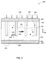
- FIG. 2 is a diagrammatic illustration of a PV cell 200 in accordance with one embodiment of the invention, shown in side cross-sectional view.
- the PV cell 200 includes a plurality of ultrafine structures 202 comprising an n-type material, which plurality of ultrafine structures 202 are coupled electrically and mechanically to a subtrate 208. Furthermore, the plurality of ultrafine structures 202 are embedded within, and in electrical communication with, the polycrystalline photo-active absorber layer 204, which photo-active absorber layer 204 comprises p-type CdTe. Furthermore, the photo-active absorber layer 204, is in electrical communication with an electrode layer 234, which electrode layer 234 comprises a p-type semiconductor.
- the subtrate 208 may be any metallic, or semiconducting template that is suitable for the growth of ultrafine structures, and also possesses appropriate electrical characteristics to serve as an electrode, as also appropriate optical characteristics to serve as an optical window layer. In other words therefore, the substrate 208 should possess appropriate electro-optical characteristics to serve also as an optical-window-electrode layer (OWE) layer.
- the substrate 208 may be formed as a layer of a transparent conducting oxide on glass.
- Non-limiting examples of transparent conducting oxides include, indium tin oxide (ITO), indium zinc oxide (IZO), aluminum zinc oxide (AZO), amorphous zinc oxide (aZO), cadmium stannate (Cd 2 SnO 4 ) zinc oxide (ZnO), tin oxide (SnO 2 ), indium oxide (In 2 O 3 ), cadmium tin oxide, fluorinated tin oxide, and combinations thereof.
- the substrate 208 includes n-type cadmium sulphide (CdS) or any other appropriate n-type material having properties that allow the substrate 208 to serve as an OWE layer.
- CdS n-type cadmium sulphide
- the subtrate 208 coupled to the plurality of ultrafine structures 202 serves as the negative electrode for an electrical load (not shown) connected to the PV cell 200, while the electrode layer 234 coupled to the photo-active absorber layer 204 serves as a positive electrode for the electrical load (not shown) connected to the PV cell 200.
- the plurality of ultrafine structures 202 include at least one n-type material, wherein the n-type material includes semiconductors, or transparent conducting oxides.
- a carrier density within the n-type material lies within a range from about 10 16 per cubic centimeter (/cm 3 ) to about 10 18 /cm 3 .
- a carrier density within the n-type material can be up to about 10 21 /cm 3 .
- the plurality ultrafine structures comprise an n-type material coated with an n-type semiconductor.
- Non-limiting examples of the n-type semiconductor include n-type cadmium sulphide.
- the n-type semiconductor has a carrier density of that lies within a range from about 10 15 /cm 3 to about 10 19 /cm 3 . In one embodiment of the invention, the n-type semiconductor has a carrier density that lies within a range from about 10 15 /cm 3 to about 2 x 10 20 .
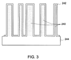
- FIG. 3 is a diagrammatic illustration of a plurality of metallic ultrafine structures 240 of type 202 having a conformal coating 242, wherein the conformal coating 242 comprises an n-type semiconductor.
- PV cell embodiments including a plurality of ultrafine structures including a plurality of metallic ultrafine structures wherein at least a portion of the plurality of metallic ultrafine structures have a conformal coating comprising a n-type semiconductor fall within the purview of the present invention.
- An electric field 218 is generated across a p-n junction 220 between the photo-active absorber layer 204 comprising p-type CdTe and the plurality of ultrafine structures 202 comprising a n-type semiconductor, according to principles that would be known to one of skill in the art of photovoltaics. In the embodiment presently under discussion, the electric field 218 would be directed substantially "inwards" from bulk portions 226 of the p-type CdTe layer 204 towards the individual ultrafine structures of the plurality of ultrafme structures 202.
- the p-n junction 220 is “distributed,” along the interface regions 228 between the plurality of ultrafme structures 202, and the bulk portions 226 of the photo-active absorber layer 204.
- the interface regions 228 are “spread-out” across the bulk of the photo-active absorber layer 204.
- PV cell designs according to embodiments of the present invention possess several enhancements over present generation PV cell designs, as are now discussed.
- a light energy flux 238 incident on the substrate 208 continues on to the photo-active absorber layer 204, wherein it causes the generation of electron-hole pairs.
- reference numeral 232 indicates an example of such a photo-generated electron. Due to the distributed nature of the p-n junction 220, the "average" distance 230 between a photo-generated charge carrier, for instance, the photo-generated electron 232, and the p-n junction 220, decreases (over for instance, the average distance 122 between the p-n junction interface 120 ( FIG. 1 ) and photo-generated charge carriers, for instance the electron 116 as depicted in FIG. 1 ).
- the thickness of the photo-active absorber layer 204 can be up to about 10 micrometers. In one embodiment of the invention, the thickness of the photo-active absorber layer 204 can be up to about 5 micrometer. In another embodiment of the invention, the thickness of the photo-active absorber layer 204 can be up to about 3 micrometer.
- embodiments of the present invention may be exempt from the requirement of a n-type CdS optical window layer (of type 104) in order to perform a photovoltaic function.
- the substrate 208 may itself be formed from a material (such as a transparent conducting oxide) having appropriate electrical and optical characteristics to serve as an OWE layer.
- Embodiments of the invention include PV cells (for instance, of type 200) that are capable of generating an open circuit voltage "V OC " of up to about 0.85 Volt. Alternate embodiments of the invention include PV cells (for instance, of type 200) that are capable of generating a short circuit current density "J SC " of up to about 0.025 Ampere/cm 2 .
- PV cells according to embodiments of the present invention will be capable of achieving a J SC of up to about 0.028 A/cm 2 , leading to efficiencies (for conversion of light energy to electrical energy) of greater than about 16% and up to about 20%.
- the plurality of ultrafine structures 202 include cadmium telluride (CdTe), cadmium sulphide (CdS), zinc telluride (ZnTe), zinc selenide (ZnSe), cadmium selenide (CdSe), zinc sulphide (ZnS), indium selenide (In 2 Se 3 ), indium sulphide (In 2 S 3 ), or zinc oxyhydrate.
- at least a portion of the plurality of ultrafine structures 202 comprise a structure comprising at least one nanowire, or at least one nanotube, or at least one quantum wire, or at least one quantum dot, or at least one nanowall.
- individual ultrafine structures of the plurality of ultrafine structures 202 may be formed as a "pillar," or "string" of quantum dots.
- at least one physical dimension of at least a portion of the plurality of ultrafine structures is less than about 1 micrometer. In more particular embodiments of the invention, at least one physical dimension of at least a portion of the plurality of ultrafine structures is less than about 500 nanometers. In more particular embodiments of the invention, at least one physical dimension of at least a portion of the plurality of ultrafine structures is less than about 200 nanometers. In more particular embodiments of the invention, at least one physical dimension of at least a portion of the plurality of ultrafine structures is less than about 100 nanometers.
- the plurality of ultrafine structures include an n-type semiconductor material.
- the plurality of ultrafine structures comprise a material having a semiconducting band-gap substantially greater than the semiconducting band-gap of the p-type CdTe of the photo-active absorber layer 204.
- the plurality of ultrafme structures comprise a material having a semiconducting band-gap substantially equal to the semiconducting band-gap of the p-type CdTe from which is comprised the photo-active absorber layer 204.
- a carrier density within the photo-active absorber layer 204 lies within a range from about 10 14 /cm 3 to about 10 16 /cm 3 . In one embodiment of the invention, a carrier density within the plurality of ultrafine structures 202 lies within a range from about 10 15 /cm 3 to about 10 19 /cm 3 .
- the PV cell 200 further includes a contact electrode layer 250 comprising a p-type material in electrical contact with the photo-active absorber photo-active absorber layer 204 comprising p-type CdTe.
- the contact electrode layer 250 comprises a transparent conducting oxide.
- the contact electrode layer 250 is configured to function as an optical-window-electrode (OWE) layer.
- OBE optical-window-electrode
- the contact electrode layer 250 has higher carrier density than the photo-active absorber layer 204.
- the contact electrode layer 250 has a carrier density greater than about 5 x 10 17 /cm 3 .
- the contact electrode layer 250 comprises a material comprising BaCuXF, wherein 'X' comprises sulphur, selenium, or tellurium. In one embodiment of the invention, the contact electrode layer 250 comprises a material comprising LaCuOX, wherein 'X' comprises sulphur, selenium, or tellurium. In one embodiment of the invention the contact electrode layer 250 comprises a material comprising XCuO(S 1-y ,Se y ), wherein 'X' comprises praseodymium, neodymium, or a lanthanide, and 'y' can assume values between zero and one. In one embodiment of the invention the contact electrode layer 250 comprises Sr 2 Cu 2 ZnO 2 S 2 or Sr 2 CuGaO 3 S.
- embodiments of the invention include, a PV cell (for instance, of type 200) including, a plurality of ultrafme structures (for instance, of type 202) electrically coupled to, and embedded within, a polycrystalline photo-active absorber layer (for instance, of type 204) comprising p-type CdTe.
- FIG. 3 is a diagrammatic illustration 300 of a portion 210 of the PV cell 200 shown in FIG. 2 .
- Reference numerals 302, and 304 indicate respectively portions of the photo-active absorber layer 204, and of the subtrate 208, while reference numeral 306 indicates a single ultrafine structure of the plurality of ultrafine structures 202.
- Reference numeral 334 indicates a portion of the contact electrode layer 250.
- a portion of the electric field 218 is indicated via reference numeral 316, which electric field portion 316, according to principles that would be known to one of skill in the art of photovoltaics, points inwards from a bulk portion 302 of the photo-active absorber layer 304 (204) towards the ultrafine structure 306 of the plurality of ultrafine structures 202.
- electric field portion 316 points substantially "outwards" from the single ultrafine structure 306 and towards a bulk portion 302 of the photo-active absorber layer 204. At least a portion of light energy flux 308 incident on the subtrate 304 (208) continues on to the photo-active absorber layer 302 (204) where it causes the generation of electron-hole pairs. It is pointed out that, bifacial PV cell embodiments, wherein a light energy flux 336 may be incident on the contact electrode layer 334 (250), and which light energy flux 336 will also cause a generation of electron-hole pairs, fall within the purview of the present invention.
- an instance of such a photo-generated electron-hole pair is indicated via reference numeral 310, the electron 312 of the electron-hole pair 310 drifts, under the action of the electric field 316, towards the single ultrafine structure 306, for collection. Similarly, the hole 314 of the electron-hole pair 310 drifts, under the action of electric field 316, towards the p-type semiconductor layer 326 (234) for collection.
- the direction of drift of the electron 312 and the hole 314 are indicated via reference numerals 318 and 320 respectively.
- the general direction of drift of electrons towards the ultrafine structure 306 (202), and of the holes towards the electrode layer 326 (234) are indicated by reference numerals 322 and 324 respectively.
- the subtrate 304 (208) coupled to the ultrafme structure 306 (202) comprising an n-type material serves as the negative electrode of the PV cell 200
- the electrode layer 326 (234) comprising a p-type semiconductor and coupled to the photo-active absorber layer 302 (204) comprising p-type CdTe serves as the positive electrode of the PV cell 200.
- Bifacial PV cell embodiments wherein light energy flux incident upon the substrate 304 (208), as well as upon the p-type contact electrode layer 334 (250), is used for photo-current generation, fall within the purview of the present invention.
- the substrate 304 (208) as well as the contact electrode layer 334 (250) serve as OWE layers.
- a light energy flux 308, and light energy flux 340 may be allowed to be incident, on the substrate 304 (208), and on the contact electrode layer 334 (250), to result in generation of electron-hole pairs.
- the plurality of ultrafine structures 202 serve to collect the photo-generated holes generated substantially within the photo-active layer 204.
- the plurality of ultrafine structures 202 are embedded with the photo-active absorber layer 204. It is noted that the photo-current generation within embodiments of the present invention takes place substantially within the photo-active absorber layer, while the plurality of ultrafine structures 202 serve to extract at least a portion of the photo-current. (However, the inventors recognize that photo-current generation likely occurs also within the plurality of ultrafme structures 202.
- the typical spacing between individual ultrafine structures of the plurality of ultrafine structures 202 may advantageously be at least of the order of twice the depletion length scale of the p-n junction 220. Such spacing would likely result in a diminution in overlap of electric fields within the depletion regions surrounding and corresponding to the individual ultrafine structures.
- embodiments of the invention include a photovoltaic solar cell (for instance, of type 200), including an OWE layer (for instance, a subtrate of type 208), a plurality of ultrafme structures (for instance, ultrafine structures of type 202) electrically coupled to, and embedded within and substantially along a thickness direction (for instance, of type 224) of, a polycrystalline photo-active absorber layer (for instance, of type 204) comprising p-type CdTe, and a electrode layer (for instance, of type 234) comprising p-type semiconductor.
- OWE layer for instance, a subtrate of type 208
- ultrafme structures for instance, ultrafine structures of type 202
- a polycrystalline photo-active absorber layer for instance, of type 204 comprising p-type CdTe
- a electrode layer for instance, of type 234) comprising p-type semiconductor.
- embodiments of the invention include a PV cell (similar in structure to the PV cell 200) including a plurality of ultrafine structures (for instance, of type 202) embedded within a photo-active absorber layer (similar in structure to the photo-active absorber layer 204) comprising a p-type compound semiconductor.
- compound semiconductors include gallium arsenide, indium gallium arsenide, copper indium gallium selenide, Cu(In,Ga,Al,Ag)(S,Se) 2 , copper zinc tin sulphide, and combinations thereof.
Landscapes
- Photovoltaic Devices (AREA)
Applications Claiming Priority (1)
| Application Number | Priority Date | Filing Date | Title |
|---|---|---|---|
| US12/645,618 US20110146788A1 (en) | 2009-12-23 | 2009-12-23 | Photovoltaic cell |
Publications (2)
| Publication Number | Publication Date |
|---|---|
| EP2339643A2 true EP2339643A2 (de) | 2011-06-29 |
| EP2339643A3 EP2339643A3 (de) | 2015-06-10 |
Family
ID=44012378
Family Applications (1)
| Application Number | Title | Priority Date | Filing Date |
|---|---|---|---|
| EP10196024.3A Withdrawn EP2339643A3 (de) | 2009-12-23 | 2010-12-20 | Photovoltaikzelle |
Country Status (4)
| Country | Link |
|---|---|
| US (1) | US20110146788A1 (de) |
| EP (1) | EP2339643A3 (de) |
| CN (1) | CN102136516A (de) |
| AU (1) | AU2010257429A1 (de) |
Cited By (3)
| Publication number | Priority date | Publication date | Assignee | Title |
|---|---|---|---|---|
| WO2018146579A1 (ja) * | 2017-02-10 | 2018-08-16 | 株式会社半導体エネルギー研究所 | 光電変換素子、撮像装置、電子機器及び光電変換素子の作製方法 |
| WO2021167227A1 (ko) * | 2020-02-21 | 2021-08-26 | 고려대학교 산학협력단 | 태양 전지 모듈 |
| EP2615649B1 (de) * | 2012-01-10 | 2022-09-28 | The Boeing Company | Seitliche Solarzellenstruktur |
Families Citing this family (2)
| Publication number | Priority date | Publication date | Assignee | Title |
|---|---|---|---|---|
| US9324898B2 (en) | 2012-09-25 | 2016-04-26 | Alliance For Sustainable Energy, Llc | Varying cadmium telluride growth temperature during deposition to increase solar cell reliability |
| CN104465807B (zh) * | 2014-12-18 | 2016-06-22 | 商丘师范学院 | 一种czts纳米阵列薄膜太阳能光伏电池及其制备方法 |
Family Cites Families (21)
| Publication number | Priority date | Publication date | Assignee | Title |
|---|---|---|---|---|
| FR2336804A1 (fr) * | 1975-12-23 | 1977-07-22 | Telecommunications Sa | Perfectionnements apportes aux dispositifs semi-conducteurs, notamment aux detecteurs photovoltaiques comprenant un substrat a base d'un alliage cdxhg1-xte, et procede de fabrication d'un tel dispositif perfectionne |
| JPS5687381A (en) * | 1979-12-19 | 1981-07-15 | Ricoh Co Ltd | Photoelectric conversion element |
| US4367368A (en) * | 1981-05-15 | 1983-01-04 | University Patents Inc. | Solar cell |
| US4529832A (en) * | 1984-02-21 | 1985-07-16 | Savin Corporation | Lead-cadmium-sulphide solar cell |
| DE69941294D1 (de) * | 1998-09-18 | 2009-10-01 | Univ Rice William M | Chemische derivatisierung von einwandigen kohlenstoffnanoröhren um ihre solvatation zu erleichtern und verwendung derivatisierter nanoröhren |
| JP2004510678A (ja) * | 2000-10-04 | 2004-04-08 | ザ ボード オブ トラスティーズ オブ ザ ユニバーシティ オブ アーカンソー | コロイドナノ結晶の合成 |
| US6706959B2 (en) * | 2000-11-24 | 2004-03-16 | Clean Venture 21 Corporation | Photovoltaic apparatus and mass-producing apparatus for mass-producing spherical semiconductor particles |
| US6946597B2 (en) * | 2002-06-22 | 2005-09-20 | Nanosular, Inc. | Photovoltaic devices fabricated by growth from porous template |
| JP2005538573A (ja) * | 2002-09-05 | 2005-12-15 | ナノシス・インク. | ナノ構造及びナノ複合材をベースとする組成物 |
| US7605327B2 (en) * | 2003-05-21 | 2009-10-20 | Nanosolar, Inc. | Photovoltaic devices fabricated from nanostructured template |
| US7462774B2 (en) * | 2003-05-21 | 2008-12-09 | Nanosolar, Inc. | Photovoltaic devices fabricated from insulating nanostructured template |
| US7227066B1 (en) * | 2004-04-21 | 2007-06-05 | Nanosolar, Inc. | Polycrystalline optoelectronic devices based on templating technique |
| US20060207647A1 (en) * | 2005-03-16 | 2006-09-21 | General Electric Company | High efficiency inorganic nanorod-enhanced photovoltaic devices |
| JP5324222B2 (ja) * | 2005-08-22 | 2013-10-23 | キュー・ワン・ナノシステムズ・インコーポレイテッド | ナノ構造およびそれを実施する光起電力セル |
| US7635600B2 (en) * | 2005-11-16 | 2009-12-22 | Sharp Laboratories Of America, Inc. | Photovoltaic structure with a conductive nanowire array electrode |
| EP1994812B1 (de) * | 2006-03-03 | 2013-07-10 | Tte Technology, Inc. | Kühlstruktur für eine wärmeerzeugende einrichtung |
| WO2007120905A2 (en) * | 2006-04-18 | 2007-10-25 | Dow Corning Corporation | Cadmium telluride-based photovoltaic device and method of preparing the same |
| EP1892769A2 (de) * | 2006-08-25 | 2008-02-27 | General Electric Company | Nanodraht-Photovoltaikgeräte mit konformem Einzelübergang |
| US7893348B2 (en) * | 2006-08-25 | 2011-02-22 | General Electric Company | Nanowires in thin-film silicon solar cells |
| US7999176B2 (en) * | 2007-05-08 | 2011-08-16 | Vanguard Solar, Inc. | Nanostructured solar cells |
| WO2009094366A1 (en) * | 2008-01-24 | 2009-07-30 | University Of Toledo | Nanodipole photovoltaic devices, methods of making and methods of use thereof |
-
2009
- 2009-12-23 US US12/645,618 patent/US20110146788A1/en not_active Abandoned
-
2010
- 2010-12-20 EP EP10196024.3A patent/EP2339643A3/de not_active Withdrawn
- 2010-12-23 AU AU2010257429A patent/AU2010257429A1/en not_active Abandoned
- 2010-12-23 CN CN2010106251630A patent/CN102136516A/zh active Pending
Non-Patent Citations (1)
| Title |
|---|
| None |
Cited By (4)
| Publication number | Priority date | Publication date | Assignee | Title |
|---|---|---|---|---|
| EP2615649B1 (de) * | 2012-01-10 | 2022-09-28 | The Boeing Company | Seitliche Solarzellenstruktur |
| WO2018146579A1 (ja) * | 2017-02-10 | 2018-08-16 | 株式会社半導体エネルギー研究所 | 光電変換素子、撮像装置、電子機器及び光電変換素子の作製方法 |
| WO2021167227A1 (ko) * | 2020-02-21 | 2021-08-26 | 고려대학교 산학협력단 | 태양 전지 모듈 |
| US12046691B2 (en) | 2020-02-21 | 2024-07-23 | Korea University Research And Business Foundation | Photovoltaic module |
Also Published As
| Publication number | Publication date |
|---|---|
| AU2010257429A1 (en) | 2011-07-07 |
| CN102136516A (zh) | 2011-07-27 |
| EP2339643A3 (de) | 2015-06-10 |
| US20110146788A1 (en) | 2011-06-23 |
Similar Documents
| Publication | Publication Date | Title |
|---|---|---|
| JP6689456B2 (ja) | 透明トンネル接合を有する光起電力デバイス | |
| US10290755B1 (en) | High efficiency photovoltaic cells and manufacturing thereof | |
| US20170271622A1 (en) | High efficiency thin film tandem solar cells and other semiconductor devices | |
| US11380808B1 (en) | High efficiency quantum dot sensitized thin film solar cell with absorber layer | |
| CN107112376A (zh) | 双层光伏设备 | |
| WO2019113490A1 (en) | High absorption, photo induced resonance energy transfer electromagnetic energy collector | |
| US20150200322A1 (en) | Semiconductor Heterojunction Photovoltaic Solar Cell with a Charge Blocking Layer | |
| US20070204901A1 (en) | Photovoltaic cells based on nano or micro-scale structures | |
| EP2339643A2 (de) | Photovoltaikzelle | |
| US10256362B2 (en) | Flexible silicon infrared emitter | |
| Gupta et al. | Simulation studies of CZT (S, Se) single and tandem junction solar cells towards possibilities for higher efficiencies up to 22% | |
| EP2341551A2 (de) | Hybride Solarzellen | |
| EP2339644A2 (de) | Fotovoltaische Zelle | |
| US20190312167A1 (en) | Photovoltaic Cells | |
| KR101412150B1 (ko) | 탠덤 구조 cigs 태양전지 및 그 제조방법 | |
| US20190229226A1 (en) | Wide Band-Gap II-VI Heterojunction Solar Cell for Use In Tandem Structure | |
| JP7627056B2 (ja) | 直接遷移型半導体ソーラ装置の改善 | |
| CN112713207A (zh) | 一种光伏电池 | |
| CN110289326A (zh) | 一种光伏电池 | |
| US9349901B2 (en) | Solar cell apparatus and method of fabricating the same | |
| HK1236677A1 (en) | Dual layer photovoltaic device | |
| TW200929570A (en) | Solar cell |
Legal Events
| Date | Code | Title | Description |
|---|---|---|---|
| PUAI | Public reference made under article 153(3) epc to a published international application that has entered the european phase |
Free format text: ORIGINAL CODE: 0009012 |
|
| AK | Designated contracting states |
Kind code of ref document: A2 Designated state(s): AL AT BE BG CH CY CZ DE DK EE ES FI FR GB GR HR HU IE IS IT LI LT LU LV MC MK MT NL NO PL PT RO RS SE SI SK SM TR |
|
| AX | Request for extension of the european patent |
Extension state: BA ME |
|
| RAP1 | Party data changed (applicant data changed or rights of an application transferred) |
Owner name: FIRST SOLAR MALAYSIA SDN.BHD |
|
| PUAL | Search report despatched |
Free format text: ORIGINAL CODE: 0009013 |
|
| AK | Designated contracting states |
Kind code of ref document: A3 Designated state(s): AL AT BE BG CH CY CZ DE DK EE ES FI FR GB GR HR HU IE IS IT LI LT LU LV MC MK MT NL NO PL PT RO RS SE SI SK SM TR |
|
| AX | Request for extension of the european patent |
Extension state: BA ME |
|
| RIC1 | Information provided on ipc code assigned before grant |
Ipc: H01L 31/072 20120101ALI20150504BHEP Ipc: H01L 31/0352 20060101AFI20150504BHEP Ipc: H01L 31/18 20060101ALI20150504BHEP Ipc: H01L 31/0296 20060101ALI20150504BHEP |
|
| STAA | Information on the status of an ep patent application or granted ep patent |
Free format text: STATUS: THE APPLICATION IS DEEMED TO BE WITHDRAWN |
|
| 18D | Application deemed to be withdrawn |
Effective date: 20150211 |