EP2339644A2 - Cellule photovoltaïque - Google Patents
Cellule photovoltaïque Download PDFInfo
- Publication number
- EP2339644A2 EP2339644A2 EP20100194628 EP10194628A EP2339644A2 EP 2339644 A2 EP2339644 A2 EP 2339644A2 EP 20100194628 EP20100194628 EP 20100194628 EP 10194628 A EP10194628 A EP 10194628A EP 2339644 A2 EP2339644 A2 EP 2339644A2
- Authority
- EP
- European Patent Office
- Prior art keywords
- type
- cell
- photo
- layer
- cdte
- Prior art date
- Legal status (The legal status is an assumption and is not a legal conclusion. Google has not performed a legal analysis and makes no representation as to the accuracy of the status listed.)
- Withdrawn
Links
- 239000006096 absorbing agent Substances 0.000 claims abstract description 95
- 239000004065 semiconductor Substances 0.000 claims abstract description 59
- 150000001875 compounds Chemical class 0.000 claims abstract description 20
- MARUHZGHZWCEQU-UHFFFAOYSA-N 5-phenyl-2h-tetrazole Chemical compound C1=CC=CC=C1C1=NNN=N1 MARUHZGHZWCEQU-UHFFFAOYSA-N 0.000 claims description 99
- 230000005855 radiation Effects 0.000 claims description 10
- 230000005611 electricity Effects 0.000 claims description 9
- 229910052751 metal Inorganic materials 0.000 claims description 9
- 239000002184 metal Substances 0.000 claims description 9
- 239000011248 coating agent Substances 0.000 claims description 5
- 238000000576 coating method Methods 0.000 claims description 5
- 239000012141 concentrate Substances 0.000 claims description 3
- 230000005670 electromagnetic radiation Effects 0.000 claims description 3
- 239000000758 substrate Substances 0.000 description 21
- 230000003287 optical effect Effects 0.000 description 20
- 239000000463 material Substances 0.000 description 17
- 230000005684 electric field Effects 0.000 description 11
- 238000006243 chemical reaction Methods 0.000 description 10
- 238000009434 installation Methods 0.000 description 9
- 230000004907 flux Effects 0.000 description 8
- JBRZTFJDHDCESZ-UHFFFAOYSA-N AsGa Chemical compound [As]#[Ga] JBRZTFJDHDCESZ-UHFFFAOYSA-N 0.000 description 7
- 229910001218 Gallium arsenide Inorganic materials 0.000 description 7
- XLOMVQKBTHCTTD-UHFFFAOYSA-N Zinc monoxide Chemical compound [Zn]=O XLOMVQKBTHCTTD-UHFFFAOYSA-N 0.000 description 7
- 238000011161 development Methods 0.000 description 7
- 238000013459 approach Methods 0.000 description 6
- SKJCKYVIQGBWTN-UHFFFAOYSA-N (4-hydroxyphenyl) methanesulfonate Chemical compound CS(=O)(=O)OC1=CC=C(O)C=C1 SKJCKYVIQGBWTN-UHFFFAOYSA-N 0.000 description 5
- 229910000530 Gallium indium arsenide Inorganic materials 0.000 description 5
- KXNLCSXBJCPWGL-UHFFFAOYSA-N [Ga].[As].[In] Chemical compound [Ga].[As].[In] KXNLCSXBJCPWGL-UHFFFAOYSA-N 0.000 description 5
- 238000004891 communication Methods 0.000 description 5
- 238000010276 construction Methods 0.000 description 5
- 238000013461 design Methods 0.000 description 5
- 239000002019 doping agent Substances 0.000 description 5
- 239000002070 nanowire Substances 0.000 description 5
- 238000001228 spectrum Methods 0.000 description 5
- 230000009471 action Effects 0.000 description 4
- 230000006872 improvement Effects 0.000 description 4
- 239000002096 quantum dot Substances 0.000 description 4
- XOLBLPGZBRYERU-UHFFFAOYSA-N tin dioxide Chemical compound O=[Sn]=O XOLBLPGZBRYERU-UHFFFAOYSA-N 0.000 description 4
- PFNQVRZLDWYSCW-UHFFFAOYSA-N (fluoren-9-ylideneamino) n-naphthalen-1-ylcarbamate Chemical compound C12=CC=CC=C2C2=CC=CC=C2C1=NOC(=O)NC1=CC=CC2=CC=CC=C12 PFNQVRZLDWYSCW-UHFFFAOYSA-N 0.000 description 3
- WUPHOULIZUERAE-UHFFFAOYSA-N 3-(oxolan-2-yl)propanoic acid Chemical compound OC(=O)CCC1CCCO1 WUPHOULIZUERAE-UHFFFAOYSA-N 0.000 description 3
- GPXJNWSHGFTCBW-UHFFFAOYSA-N Indium phosphide Chemical compound [In]#P GPXJNWSHGFTCBW-UHFFFAOYSA-N 0.000 description 3
- 239000005083 Zinc sulfide Substances 0.000 description 3
- KTSFMFGEAAANTF-UHFFFAOYSA-N [Cu].[Se].[Se].[In] Chemical compound [Cu].[Se].[Se].[In] KTSFMFGEAAANTF-UHFFFAOYSA-N 0.000 description 3
- 239000011149 active material Substances 0.000 description 3
- 229910052980 cadmium sulfide Inorganic materials 0.000 description 3
- LCUOIYYHNRBAFS-UHFFFAOYSA-N copper;sulfanylideneindium Chemical compound [Cu].[In]=S LCUOIYYHNRBAFS-UHFFFAOYSA-N 0.000 description 3
- 230000007812 deficiency Effects 0.000 description 3
- JAONJTDQXUSBGG-UHFFFAOYSA-N dialuminum;dizinc;oxygen(2-) Chemical compound [O-2].[O-2].[O-2].[O-2].[O-2].[Al+3].[Al+3].[Zn+2].[Zn+2] JAONJTDQXUSBGG-UHFFFAOYSA-N 0.000 description 3
- 229910003437 indium oxide Inorganic materials 0.000 description 3
- AKUCEXGLFUSJCD-UHFFFAOYSA-N indium(3+);selenium(2-) Chemical compound [Se-2].[Se-2].[Se-2].[In+3].[In+3] AKUCEXGLFUSJCD-UHFFFAOYSA-N 0.000 description 3
- PJXISJQVUVHSOJ-UHFFFAOYSA-N indium(iii) oxide Chemical compound [O-2].[O-2].[O-2].[In+3].[In+3] PJXISJQVUVHSOJ-UHFFFAOYSA-N 0.000 description 3
- 239000002071 nanotube Substances 0.000 description 3
- 239000011787 zinc oxide Substances 0.000 description 3
- 229910052984 zinc sulfide Inorganic materials 0.000 description 3
- 229910000661 Mercury cadmium telluride Inorganic materials 0.000 description 2
- XUIMIQQOPSSXEZ-UHFFFAOYSA-N Silicon Chemical compound [Si] XUIMIQQOPSSXEZ-UHFFFAOYSA-N 0.000 description 2
- 229910052793 cadmium Inorganic materials 0.000 description 2
- MCMSPRNYOJJPIZ-UHFFFAOYSA-N cadmium;mercury;tellurium Chemical compound [Cd]=[Te]=[Hg] MCMSPRNYOJJPIZ-UHFFFAOYSA-N 0.000 description 2
- BEQNOZDXPONEMR-UHFFFAOYSA-N cadmium;oxotin Chemical compound [Cd].[Sn]=O BEQNOZDXPONEMR-UHFFFAOYSA-N 0.000 description 2
- 230000000694 effects Effects 0.000 description 2
- 229910052732 germanium Inorganic materials 0.000 description 2
- GNPVGFCGXDBREM-UHFFFAOYSA-N germanium atom Chemical compound [Ge] GNPVGFCGXDBREM-UHFFFAOYSA-N 0.000 description 2
- 238000010438 heat treatment Methods 0.000 description 2
- AMGQUBHHOARCQH-UHFFFAOYSA-N indium;oxotin Chemical compound [In].[Sn]=O AMGQUBHHOARCQH-UHFFFAOYSA-N 0.000 description 2
- VNWKTOKETHGBQD-UHFFFAOYSA-N methane Chemical compound C VNWKTOKETHGBQD-UHFFFAOYSA-N 0.000 description 2
- 239000000203 mixture Substances 0.000 description 2
- 230000000704 physical effect Effects 0.000 description 2
- 238000012827 research and development Methods 0.000 description 2
- 229910052710 silicon Inorganic materials 0.000 description 2
- 239000010703 silicon Substances 0.000 description 2
- 229940071182 stannate Drugs 0.000 description 2
- 229910001887 tin oxide Inorganic materials 0.000 description 2
- QHGNHLZPVBIIPX-UHFFFAOYSA-N tin(ii) oxide Chemical class [Sn]=O QHGNHLZPVBIIPX-UHFFFAOYSA-N 0.000 description 2
- YVTHLONGBIQYBO-UHFFFAOYSA-N zinc indium(3+) oxygen(2-) Chemical compound [O--].[Zn++].[In+3] YVTHLONGBIQYBO-UHFFFAOYSA-N 0.000 description 2
- DRDVZXDWVBGGMH-UHFFFAOYSA-N zinc;sulfide Chemical compound [S-2].[Zn+2] DRDVZXDWVBGGMH-UHFFFAOYSA-N 0.000 description 2
- ZOXJGFHDIHLPTG-UHFFFAOYSA-N Boron Chemical compound [B] ZOXJGFHDIHLPTG-UHFFFAOYSA-N 0.000 description 1
- 230000004075 alteration Effects 0.000 description 1
- 229910052782 aluminium Inorganic materials 0.000 description 1
- XAGFODPZIPBFFR-UHFFFAOYSA-N aluminium Chemical compound [Al] XAGFODPZIPBFFR-UHFFFAOYSA-N 0.000 description 1
- 229910052787 antimony Inorganic materials 0.000 description 1
- WATWJIUSRGPENY-UHFFFAOYSA-N antimony atom Chemical compound [Sb] WATWJIUSRGPENY-UHFFFAOYSA-N 0.000 description 1
- 229910052785 arsenic Inorganic materials 0.000 description 1
- RQNWIZPPADIBDY-UHFFFAOYSA-N arsenic atom Chemical compound [As] RQNWIZPPADIBDY-UHFFFAOYSA-N 0.000 description 1
- 230000005540 biological transmission Effects 0.000 description 1
- 229910052796 boron Inorganic materials 0.000 description 1
- AQCDIIAORKRFCD-UHFFFAOYSA-N cadmium selenide Chemical compound [Cd]=[Se] AQCDIIAORKRFCD-UHFFFAOYSA-N 0.000 description 1
- UHYPYGJEEGLRJD-UHFFFAOYSA-N cadmium(2+);selenium(2-) Chemical compound [Se-2].[Cd+2] UHYPYGJEEGLRJD-UHFFFAOYSA-N 0.000 description 1
- 239000003245 coal Substances 0.000 description 1
- 239000003989 dielectric material Substances 0.000 description 1
- BHEPBYXIRTUNPN-UHFFFAOYSA-N hydridophosphorus(.) (triplet) Chemical compound [PH] BHEPBYXIRTUNPN-UHFFFAOYSA-N 0.000 description 1
- SIXIBASSFIFHDK-UHFFFAOYSA-N indium(3+);trisulfide Chemical compound [S-2].[S-2].[S-2].[In+3].[In+3] SIXIBASSFIFHDK-UHFFFAOYSA-N 0.000 description 1
- 238000000034 method Methods 0.000 description 1
- 239000003345 natural gas Substances 0.000 description 1
- 238000002161 passivation Methods 0.000 description 1
- 238000013082 photovoltaic technology Methods 0.000 description 1
- 239000011148 porous material Substances 0.000 description 1
- -1 quantum wires Substances 0.000 description 1
- 238000006467 substitution reaction Methods 0.000 description 1
- GKCNVZWZCYIBPR-UHFFFAOYSA-N sulfanylideneindium Chemical compound [In]=S GKCNVZWZCYIBPR-UHFFFAOYSA-N 0.000 description 1
- 239000010409 thin film Substances 0.000 description 1
Images


Classifications
-
- H—ELECTRICITY
- H10—SEMICONDUCTOR DEVICES; ELECTRIC SOLID-STATE DEVICES NOT OTHERWISE PROVIDED FOR
- H10F—INORGANIC SEMICONDUCTOR DEVICES SENSITIVE TO INFRARED RADIATION, LIGHT, ELECTROMAGNETIC RADIATION OF SHORTER WAVELENGTH OR CORPUSCULAR RADIATION
- H10F77/00—Constructional details of devices covered by this subclass
- H10F77/10—Semiconductor bodies
- H10F77/14—Shape of semiconductor bodies; Shapes, relative sizes or dispositions of semiconductor regions within semiconductor bodies
-
- H—ELECTRICITY
- H10—SEMICONDUCTOR DEVICES; ELECTRIC SOLID-STATE DEVICES NOT OTHERWISE PROVIDED FOR
- H10F—INORGANIC SEMICONDUCTOR DEVICES SENSITIVE TO INFRARED RADIATION, LIGHT, ELECTROMAGNETIC RADIATION OF SHORTER WAVELENGTH OR CORPUSCULAR RADIATION
- H10F10/00—Individual photovoltaic cells, e.g. solar cells
- H10F10/10—Individual photovoltaic cells, e.g. solar cells having potential barriers
- H10F10/16—Photovoltaic cells having only PN heterojunction potential barriers
- H10F10/162—Photovoltaic cells having only PN heterojunction potential barriers comprising only Group II-VI materials, e.g. CdS/CdTe photovoltaic cells
-
- H—ELECTRICITY
- H10—SEMICONDUCTOR DEVICES; ELECTRIC SOLID-STATE DEVICES NOT OTHERWISE PROVIDED FOR
- H10F—INORGANIC SEMICONDUCTOR DEVICES SENSITIVE TO INFRARED RADIATION, LIGHT, ELECTROMAGNETIC RADIATION OF SHORTER WAVELENGTH OR CORPUSCULAR RADIATION
- H10F71/00—Manufacture or treatment of devices covered by this subclass
- H10F71/125—The active layers comprising only Group II-VI materials, e.g. CdS, ZnS or CdTe
-
- H—ELECTRICITY
- H10—SEMICONDUCTOR DEVICES; ELECTRIC SOLID-STATE DEVICES NOT OTHERWISE PROVIDED FOR
- H10F—INORGANIC SEMICONDUCTOR DEVICES SENSITIVE TO INFRARED RADIATION, LIGHT, ELECTROMAGNETIC RADIATION OF SHORTER WAVELENGTH OR CORPUSCULAR RADIATION
- H10F77/00—Constructional details of devices covered by this subclass
- H10F77/10—Semiconductor bodies
- H10F77/14—Shape of semiconductor bodies; Shapes, relative sizes or dispositions of semiconductor regions within semiconductor bodies
- H10F77/143—Shape of semiconductor bodies; Shapes, relative sizes or dispositions of semiconductor regions within semiconductor bodies comprising quantum structures
- H10F77/1437—Quantum wires or nanorods
-
- Y—GENERAL TAGGING OF NEW TECHNOLOGICAL DEVELOPMENTS; GENERAL TAGGING OF CROSS-SECTIONAL TECHNOLOGIES SPANNING OVER SEVERAL SECTIONS OF THE IPC; TECHNICAL SUBJECTS COVERED BY FORMER USPC CROSS-REFERENCE ART COLLECTIONS [XRACs] AND DIGESTS
- Y02—TECHNOLOGIES OR APPLICATIONS FOR MITIGATION OR ADAPTATION AGAINST CLIMATE CHANGE
- Y02E—REDUCTION OF GREENHOUSE GAS [GHG] EMISSIONS, RELATED TO ENERGY GENERATION, TRANSMISSION OR DISTRIBUTION
- Y02E10/00—Energy generation through renewable energy sources
- Y02E10/50—Photovoltaic [PV] energy
- Y02E10/543—Solar cells from Group II-VI materials
Definitions
- the invention relates generally to the area of photovoltaic (PV) cells. More specifically, the invention relates to the area of PV cells wherein the photo-active absorber material employed is a compound semiconductor such as cadmium telluride (CdTe).
- the photo-active absorber material employed is a compound semiconductor such as cadmium telluride (CdTe).
- the solar spectrum "sunlight” contains a distribution of intensity as a function of frequency. It can be shown that the conversion efficiency for utilizing sunlight to obtain electricity via semiconductors is optimized for semiconducting band-gaps in the range vicinity of about 1.4-1.5 electron volt (eV).
- the semiconducting band-gap of CdTe is a good match for this requirement.
- PV cells including CdTe as the photo-active material may be referred to as "CdTe PV cells.”
- Improvement in the CdTe PV efficiency will likely result in an improvement in overall efficiency of CdTe PV installations. Such improvement will likely enhance the competitiveness of CdTe PV installations compared to traditional methods of generating electricity such as from natural gas, or coal. It is evident that improvement in overall efficiency will likely enable CdTe PV technology to successfully penetrate markets where small-scale area confined installations are required, such as markets for domestic PV installations.
- a CdTe PV cell that is capable of conversion efficiencies greater than about 16% would therefore be highly desirable.
- Various embodiments of the invention are directed to a photovoltaic cell.
- a photovoltaic (PV) cell comprising, a plurality of ultrafine structures embedded within a photo-active absorber layer comprising n-type cadmium telluride (CdTe).
- a photovoltaic (PV) cell comprising, a plurality of ultrafine structures embedded within a photo-active absorber layer comprising a n-type compound semiconductor.
- An electricity generating system comprising, a plurality of ultrafine structures comprising a semiconductor having a doping of a first type embedded within a photo-active absorber layer comprising CdTe having a doping of a second type.
- a solar cell comprising, an optical-window-electrode (OWE) layer, a plurality of ultrafine structures comprising a p-type semiconductor embedded within and substantially along a thickness direction of a photo-active absorber layer comprising n-type cadmium telluride (CdTe), and an electrode layer comprising a metal.
- OBE optical-window-electrode
- CdTe n-type cadmium telluride
- a photovoltaic (PV) cell comprising, an optical-window-electrode (OWE) layer, a plurality of ultrafine structures comprising a p-type semiconductor embedded within and substantially along a thickness direction of a photo-active absorber layer comprising n-type cadmium telluride (CdTe), an electrode layer comprising a metal in electrical contact with at least a portion of the plurality of ultrafine structures, and a dielectric layer mediate the photo-active absorber layer and the electrode layer.
- OLED optical-window-electrode
- a PV system comprising, at least one PV module comprising, a PV cell comprising a plurality of ultrafine structures embedded within a photo-active absorber layer comprising a n-type compound semiconductor, and a radiation concentrator disposed to concentrate electromagnetic radiation at the PV cell.
- embodiments of the invention are directed to improved photovoltaic (PV) cell designs.
- PV photovoltaic
- Particular embodiments of the invention proposed here provide for a PV cell including a photo-active absorber layer including n-type CdTe, and having an efficiency that is enhanced over the efficiencies of presently available CdTe PV cells (about 16.5%).
- Embodiments of the CdTe PV cell disclosed herein may display an efficiency in excess of 20%.
- the photo-active absorber layer disclosed herein is the part of the PV cell where the conversion of electromagnetic energy of incident light, for instance, sunlight, to electrical energy occurs.
- PV cells including a photo-active absorber layer that includes compound semiconductors other than CdTe.
- compound semiconductors include indium gallium arsenide, gallium arsenide, indium phosphide, copper indium sulfide, and copper indium gallium selenide, and combinations thereof.
- the term “ultrafine structures” will be understood to include structures such as nanowires, nanotubes, quantum wires, quantum dots, nanowalls, and combinations thereof of such structures, as also any other structure capable of displaying physical properties similar to one or more physical properties of the aforementioned structures.
- the term “ultrafine structures” will be understood to include any structure wherein a smallest physical dimension of, or feature of, the structure has a spatial extent "a us " of less than about 1 micrometer.
- a "mesh,” for instance, of nanowires, wherein the mesh extends over a spatial extent in excess of a us , but wherein at least a portion of the nanowires have at least one physical dimension that is substantially less than a us is a specific non-limiting example of an ultrafine structure according to the present definition.
- ultrafine structures wherein a spatial extent, of at least some of the features, such as pores or voids, characterizing the ultrafine structures, is less than about 1 micrometer, fall within the purview of the present invention.
- the ultrafine structures may be disposed on a substrate, for instance, a thin-film, of the same material from which the ultrafine structures are formed.
- the substrate may be formed from a dielectric material, which substrate may also serve as a template for the growth of the ultrafine structures.
- PV cells including CdTe as the photo-active material may be referred to as "CdTe PV cells.”
- the type of doping (p-type or n-type) of the CdTe will be specified, although is non-limiting.
- FIG. 1 is a diagrammatic illustration of a portion 100 of a CdTe PV cell design, for the purposes of discussion of some general operational principles of PV cells.
- the portion 100 shown includes three layers, 102, 104, and 106.
- the PV cell portion 100 includes a p-type CdTe layer 102 that is disposed mediate to an n-type optical window layer 104 and an electrode layer 106.
- the interface between the p-type CdTe layer 102 and the n-type optical window layer 104 may properly be considered as a hetero-junction 112.
- An electric field 110 is generated across the hetero-junction 112 between the p-type CdTe layer 102 and the n-type optical window layer 104, according to principles that would be known to one of skill in the art of photovoltaics.
- Light energy flux 108 when it is allowed to be incident on the optical window layer 104, continues on to the CdTe layer 102, wherein the light energy is absorbed to generate electron-hole pairs, that is, the light energy is absorbed to generate electricity.
- An instance of an electron-hole pair is indicated via reference numeral 114, the hole 118 of the electron-hole pair 114 drifts, under the action of the electric field 110, towards the electrode layer 106 for collection.
- the electron 116 of the electron-hole pair 114 drifts, under the action of electric field 110, towards the n-type optical window layer 104 for collection.
- the electrode layer 106 serves as the positive electrode to an external electrical load (not shown in FIG. 1 ) that is connected to the PV cell (of which portion 100 is a part),
- n-type optical window layer 104 serves also as a negative electrode to the external electrical load that is connected to the PV cell.
- CdTe PV cells employ p-type CdTe for forming the absorber layer.
- An issue of significance in this context is that, despite several years of research and development work by the industry and academia, it has not been possible to enhance p-type doping levels within the p-type CdTe absorber layer beyond about ⁇ 2 x 10 14 per cubic centimeter (cm). This is among the factors limiting the best reported values of open circuit voltage V OC , and short circuit current density J SC , for present generation CdTe PV cells to about 0.85 Volts, and 0.025 Amperes/cm 2 , respectively. These limitations in turn have limited the best reported efficiencies for present generation CdTe PV cells to about 16.5%.
- the insight for the present invention stems from the recognition, by the inventors, that the inability to p-type dope CdTe to higher (beyond about ⁇ 2 x 10 14 /cm 3 ) levels is one of the crucial factors hampering the development of CdTe PV cells including a CdTe absorber layer with efficiencies close to the entitlement-efficiency for the solar energy spectrum.
- PV cells for instance, of type 100
- PV cells include a p-type CdTe layer as the absorber layer, and require an optical window layer to be disposed on the p-type CdTe layer, so that the interface between the optical window layer and the p-type CdTe layer forms a hetero-junction.
- materials that can simultaneously form a hetero-junction with n-type CdTe, as well as have optical characteristics that allow them to function suitably as an optical window layer.
- optical window layer when an absorber layer is fabricated from n-type CdTe, has precluded the development of high performance PV cells including an n-type CdTe absorber layer.
- Characteristics required of the optical window layer include an appropriately high band-gap in order that a sufficient portion of incident light energy may reach the absorber layer. That is, the optical window layer should have an appropriately high optical transmission.
- Other characteristics required of the optical window layer include a suitably low sheet resistance, in order to diminish series resistance losses within the optical window layer.
- embodiments of the invention disclosed herein provide approaches that have the potential to enable development of a viable PV cell design including a photo-active absorber n-type CdTe layer.
- PV cell designs according to embodiments of the present invention circumvent the problem of deficiency of suitable materials for forming an optical window layer when the absorber layer includes n-type CdTe.
- Embodiments of the present invention therefore may enable the development of a PV cell including a photo-active absorber n-type CdTe layer with an efficiency that is enhanced over the efficiency of present generation CdTe PV cells that include p-type CdTe to form the absorber layer.
- CdTe PV cells proposed herein may also possess an efficiency that approaches the entitlement-efficiency of CdTe PV cells for the solar energy spectrum.
- embodiments of the invention disclosed herein have the potential to enable development of PV cells including a photo-active absorber n-type CdTe layer with efficiencies approaching, and possibly, in excess of, about 20%.
- FIG. 2 is a diagrammatic illustration of a PV cell 200 in accordance with one embodiment of the invention, shown in "exploded" view for the sake of clarity.
- the PV cell 200 includes a plurality of ultrafine structures 202 coupled electrically and mechanically to a substrate 208, which plurality of ultrafine structures 202 are embedded within a photo-active absorber layer 204 comprising n-type CdTe.
- the plurality of ultrafine structures 202 are in electrical and mechanical contact with the photo-active absorber layer 204.
- Non-limiting examples of the physical form of the ultrafine structures include single crystalline, polycrystalline, amorphous, and combinations thereof.
- the plurality of ultrafine structures are aligned so that their long axes independently lie substantially along a thickness direction of the photo-active absorber layer.
- the plurality of ultrafine structures 202 are aligned so that their longitudinal axes 222 independently lie substantially along a thickness direction 224 of the photo-active absorber layer 204.
- the substrate 208 may be any metallic, dielectric, or semiconducting template that is suitable for the growth of ultrafine structures 202, and also possesses appropriate electrical and/or optical characteristics to serve as an electrode and/or as an optical window layer.
- a dielectric layer 232 may be disposed mediate the photo-active absorber layer 204 and the substrate 208.
- the dielectric layer 232 serves as a passivation layer.
- the plurality of ultrafine structures 202 penetrate the dielectric layer 232 to make electrical and mechanical contact with the photo-active absorber layer 204. It is clarified, however, that even as the embodiment shown in FIG. 2 includes a dielectric layer 232, PV cells, otherwise similar to PV cell 200, but which do not include a dielectric layer of type 232 fall within the purview of the present invention.
- the photo-active absorber layer 204 would be in direct electrical and mechanical contact with the substrate 208, and the composition and doping type of which substrate 208 would be substantially similar to the composition and doping type of the plurality of ultrafine structures 202.
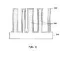
- FIG. 3 is a diagrammatic illustration of a plurality of metallic ultrafine structures 240 (of type 202), disposed on a substrate 244 (of type 208), and having a conformal coating comprising a p-type semiconductor 242.
- PV cell embodiments including a plurality of ultrafine structures including a plurality of metallic ultrafine structures wherein at least a portion of the plurality of metallic ultrafine structures have a conformal coating comprising a p-type semiconductor fall within the purview of the present invention. It is clarified that, even though in FIG. 2 , the plurality of ultrafine structures 202 disposed substantially throughout the photo-active absorber layer 204, PV cell embodiments of wherein the plurality of ultrafine structures 204 are disposed only within certain regions of the photo-active absorber layer 204, fall within the purview of the present invention. Furthermore, PV cells wherein the plurality of ultrafine structures 202 are disposed non-homogenously within the photo-active layer 204 fall within the purview of the present invention.
- the layer 204 that comprises n-type CdTe, is photo-active and serves as an absorber layer of the PV cell 200.
- the PV cell 200 further includes a first optical-window-electrode "OWE" layer 206, disposed adjacent the photo-active absorber layer 204.
- the plurality of ultrafine structures 202 comprise at least one p-type semiconductor material, and therefore an electric field 218 is generated across the p-n junction 220 between the photo-active absorber layer 204 (which photo-active absorber layer 204 includes n-type CdTe) and the plurality of ultrafine structures 202, according to principles that would be known to one of skill in the art of photovoltaics.
- the electric field 218 would be directed substantially "outwards" of the individual ultrafine structures of the plurality of ultrafine structures 202, towards bulk portions 226 of the photo-active absorber layer 204, and hence generally also towards the first OWE layer 206.
- the thickness of the photo-active absorber layer 204 can be up to about 10 micrometer. In another embodiment of the invention, the thickness of the photo-active absorber layer 204 can be up to about 5 micrometer. In yet another embodiment of the invention, the thickness of the photo-active absorber layer 204 can be up to about 2 micrometer. In one embodiment of the invention, the photo-active absorber layer 204 is polycrystalline.
- the PV cell 200 may be configured as a bifacial PV cell.
- Non-limiting approaches of configuring the PV cell 200 as a bifacial PV cell include fabricating the substrate 208 from materials having suitable optical properties, so that the substrate 208 may function as an OWE layer with functionality similar to the first OWE layer 206.
- a substrate 208, so fabricated to serve as an OWE layer may be referred to as a "second" OWE layer.
- a first non-limiting approach, therefore, to configure the substrate 208 as an OWE layer includes forming the substrate 208 to include a p-type transparent conducting oxide.
- a second non-limiting approach to configure the substrate 208 as an OWE layer includes forming the substrate 208 to include a highly doped p-type semiconductor material, which semiconductor material has a band-gap substantially larger than the band-gap of the material from which the photo-active absorber layer 204 is comprised, and a carrier density that is substantially greater than a carrier density within the ultrafine structures 202.
- This approach may require an additional layer to be disposed mediate the substrate 208 and the dielectric layer 232.
- the additional layer (not shown in FIG. 2 ) may be formed to include, depending on the carrier density of the highly doped p-type semiconductor material, either a p-type transparent conducting oxide (TCO) with a suitable carrier density, or an n-type TCO with a suitable carrier density.
- TCO transparent conducting oxide
- FIG. 4 is a diagrammatic illustration 300 of a portion 210 of the PV cell 200 shown in FIG. 2 , for the purposes of discussion of principles of operation of the PV cell 200.
- Reference numerals 302, and 304 indicate respectively portions of the photo-active absorber layer 204, and of the first OWE layer 206, while reference numeral 306 indicates a single ultrafine structure of the plurality of ultrafine structures 202.
- the single ultrafine structure 306 may include a p-type semiconductor, or it may include a metallic ultrafine structure conformally coated with a p-type semiconductor.
- a portion 336 of the p-n junction 220 between the ultrafine structure 306 and the portion 302 of the photo-active absorber layer 204 is also indicated.
- a portion of the electric field 218 is indicated via reference numeral 316, which electric field portion 316, according to principles that would be known to one of skill in the art of photovoltaics, directed substantially “outwards” from the single ultrafine structure 306 towards a bulk portion 302 of the photo-active absorber layer 204.
- electric field portion 316 points substantially “outwards” from the single ultrafine structure 306 and towards a bulk portion 302 of the photo-active absorber layer 204.
- Bifacial embodiments of the PV cell wherein a light energy flux 350 is allowed to be incident on the substrate 334 (208) (which substrate 334 has been configured to function as an OWE layer), and also cause generation of electron-hole pairs within the photo-active absorber layer 302 (204), fall within the purview of the present invention.
- the specific attributes required of the substrate 208 to realize such "bifacial" embodiments of the PV cell have been discussed earlier.
- photo-generated electrons and holes are produced within the photo-active absorber layer 302 (204).
- An instance of a photo-generated electron-hole pair is indicated via reference numeral 310, the hole 314 of which electron-hole pair 310 drifts, under the action of the electric field 316, towards the single ultrafine structure 306 for collection.
- the electron 312 of the electron-hole pair 310 drifts, under the action of electric field 316, towards the first OWE layer 304 (206) for collection.
- the direction of drift of the electron 312 and the hole 314 are indicated via reference numerals 318 and 320 respectively.
- the general direction of drift of holes towards the ultrafine structures 306 (202), and of the electrons towards the first OWE layer are indicated by reference numerals 322 and 324 respectively.
- a portion 332 of the dielectric layer 232 that lies mediate the portion 334 of the substrate 208 and the portion 302 of the photo-active absorber layer 204 is indicated.
- the plurality of ultrafine structures 202 collect the portion of a photo-current that is due to the photo-generated electron-hole pairs generated within the photo-active absorber layer 302 (204).
- the photo-current is the sum total of the current due to the photo-generated electrons and holes, for instance, of type 312 and 314 respectively.
- PV cell embodiments wherein an output current generated by the PV cell includes photo-current generated within the plurality of ultrafine structures 202 and photo-current generated within the photo-active absorber layer 204.
- the first OWE layer 304 (206) since it collects electrons, serves also as a negative electrode for the external electrical load (not shown) connected to the PV cell 200.
- the plurality of ultrafine structures 202 are embedded within the photo-active absorber layer 204. It is noted that the photo-current generation within embodiments of the present invention takes place substantially within the photo-active absorber layer, while the plurality of ultrafme structures 202 serve to extract at least a portion of the photo-current. (However, the inventors recognize that photo-current generation likely occurs also within the plurality of ultrafine structures 202.
- the typical spacing between individual ultrafine structures of the plurality of ultrafine structures 202 may advantageously be at least of the order of twice the depletion length scale of the p-n junction 220. Such spacing would likely result in a diminution in overlap of electric fields within the depletion regions surrounding and corresponding to the individual ultrafine structures.
- the layer 204 serves as a photo-active absorber layer wherein occurs a substantial portion of the photo-current generation, and within which layer 204 are embedded the plurality of ultrafine structures 202. It is similarly noted that, within embodiments of the invention disclosed herein, the plurality of ultrafine structures 202 serve to collect the photo-generated holes generated substantially within the layer 204.
- Embodiments of the invention include PV cells (for instance, of type 200) including a photo-active absorber layer (for instance, of type 204), which PV cells are potentially capable of generating an open circuit voltage "V OC " of up to about 1.05 Volt. More particular embodiments of the invention include PV cells (for instance, of type 200) including a photo-active absorber layer (for instance, of type 204), which PV cells are potentially capable of generating a short circuit current density "J SC " of up to about 0.03 Ampere/cm 2 .
- PV cells according to embodiments of the present invention may be capable of achieving conversion efficiencies (for conversion of light energy to electrical energy) substantially in excess of about 16.5%. Due to such range of achievable values of V OC and J SC , it is further envisaged that more particular PV cell embodiments according to the present invention, may be capable of achieving conversion efficiencies in excess of about 20%.
- the plurality of ultrafine structures 202 comprise a material having a semiconducting band-gap substantially greater than the semiconducting band-gap of the n-type CdTe from which is comprised the photo-active absorber layer 204. In one embodiment of the invention, the plurality of ultrafine structures 202 comprise a material having a semiconducting band-gap substantially equal to the semiconducting band-gap of the n-type CdTe from which is comprised the photo-active absorber layer 204. Furthermore, as noted earlier, the plurality of ultrafine structures 202 include at least one p-type semiconductor.
- a carrier density within the photo-active absorber layer 204 lies within a range from about 10 15 /cm 3 to about 10 17 /cm 3 . In one embodiment of the invention, a carrier density within the plurality of ultrafine structures 202 lies within a range from about 10 17 /cm 3 to about 10 20 /cm 3 .
- the first OWE layer 206 includes a transparent conducting oxide.
- the first OWE layer 206 may include one or more n-type dopants.
- transparent conducting oxides include, indium tin oxide (ITO), indium zinc oxide (IZO), aluminum zinc oxide (AZO), amorphous zinc oxide (aZO), cadmium stannate (Cd 2 SnO 4 ), zinc oxide (ZnO), tin oxide (SnO 2 ) indium oxide (In 2 O 3 ), cadmium tin oxide, fluorinated tin oxide, and combinations thereof.
- More particular embodiments of the invention include a first OWE layer including a n-type semiconductor.
- Non-limiting examples of n-type semiconductors include, cadmium sulfide (CdS), zinc telluride (ZnTe), zinc selenide (ZnSe), cadmium selenide (CdSe), zinc sulfide (ZnS), indium selenide (In 2 Se 3 ), or indium sulfide (In 2 S 3 ), and combinations thereof.
- CdS cadmium sulfide
- ZnTe zinc telluride
- ZnSe zinc selenide
- CdSe cadmium selenide
- ZnS zinc sulfide
- In 2 Se 3 indium selenide
- In 2 S 3 indium sulfide
- the plurality of ultrafine structures 202 comprise germanium, silicon, cadmium telluride, gallium arsenide, indium gallium arsenide, mercury cadmium telluride, or zinc telluride.
- at least a portion of the plurality of ultrafine structures 202 comprise a structure comprising at least one nanowire, or at least one nanotube, or at least one quantum wire, or at least one quantum dot, or at least one nanowall.
- individual ultrafine structures of the plurality of ultrafine structures 202 may be formed as a "pillar,” or "string” of quantum dots.
- at least one physical dimension of at least a portion of the plurality of ultrafine structures is less than about 1 micrometer.
- At least one physical dimension of at least a portion of the plurality of ultrafine structures is less than about 500 nanometers. In more particular embodiments of the invention, at least one physical dimension of at least a portion of the plurality of ultrafine structures is less than about 200 nanometers. In more particular embodiments of the invention, at least one physical dimension of at least a portion of the plurality of ultrafine structures is less than about 100 nanometers.
- embodiments of the invention include an electricity generating system (for instance, a PV cell of type 200) that includes a plurality of semiconductor ultrafine structures (for instance, of type 202) having a doping of a first type embedded within a photo-active absorber layer comprising CdTe (for instance, of type 204) having a doping of a second type.
- doping of the first type includes p-type doping.
- doping of the second type includes n-type doping.
- p-, and n-type doping can be achieved respectively via p-, and n-type dopants according to principles that would be known to one of skill in the art of photovoltaics.
- Non-limiting examples of p-type dopants include boron, and aluminum.
- Non-limiting examples of n-type dopants include phosphorous, arsenic, and antimony. It is remarked that p-, and n-type dopants are well known in the art.
- embodiments of the invention include a solar cell (for instance, of type 200), including an OWE layer (for instance, of type 206), a plurality of ultrafine structures comprising a p-type semiconductor (for instance, ultrafine structures of type 202) embedded within and substantially along a thickness direction (for instance, of type 224) of a photo-active absorber layer comprising n-type CdTe (for instance, of type 204), and an electrode layer comprising a metal (for instance, of type 208).
- the p-type semiconductor comprises p-type CdTe.
- a p-n junction (for instance, of type 220) between the plurality of ultrafine structures comprising a p-type semiconductor, and the photo-active absorber layer comprising n-type CdTe, is a homo-junction.
- embodiments of the invention include a PV cell (for instance, of type 200) including an OWE layer (for instance, of type 206), a plurality of ultrafine structures including a p-type semiconductor (for instance, of type 202) embedded within and substantially along a thickness direction (for instance, of type 224) of a photo-active absorber layer comprising n-type CdTe (for instance, of type 204), an electrode layer comprising a metal (for instance, of type 208) in electrical contact with at least a portion of the plurality of ultrafme structures, and a dielectric layer (for instance, of type 232) mediate the photo-active absorber layer and the electrode layer.
- a PV cell for instance, of type 200
- OWE layer for instance, of type 206
- a plurality of ultrafine structures including a p-type semiconductor (for instance, of type 202) embedded within and substantially along a thickness direction (for instance, of type 224) of a photo-active absorber layer comprising n-type CdTe (for
- embodiments of the invention include a PV cell (similar in structure to the PV cell 200) including a plurality of ultrafine structures (for instance, of type 202) embedded within a photo-active absorber layer comprising a n-type compound semiconductor (similar in structure to the photo-active absorber layer 204).
- compound semiconductors include indium gallium arsenide, gallium arsenide, indium phosphide, copper indium sulfide, and copper indium gallium selenide.
- the compound semiconductor can have a physical form selected from the group consisting of single crystalline, polycrystalline, and combinations thereof.
- FIG. 5 is a diagrammatic illustration of a PV module 400 in accordance with one embodiment of the invention.
- the PV module 400 includes at least one PV cell 402 including a plurality of ultrafine structures (for instance, of type 202) embedded within a photo-active absorber layer comprising a n-type compound semiconductor (for instance, of type 204).
- the PV module 400 also includes a radiation (that is, light energy flux) concentrator 404 disposed to direct a light energy flux 406 to be incident on, for instance, an OWE layer (for instance, of type 206) of the PV cell 402.
- a radiation (that is, light energy flux) concentrator 404 disposed to direct a light energy flux 406 to be incident on, for instance, an OWE layer (for instance, of type 206) of the PV cell 402.
- OWE layer for instance, of type 206
- PV modules including radiation concentrators (for instance, of type 404) capable of concentrating incident radiation by up to about 500 times fall within the purview of the present invention.
- Particular embodiments of the invention include PV cells wherein the photo-active absorber layer (for instance, of type 204) is substantially single crystalline.
- Particular embodiments of the invention include PV cells wherein the plurality of ultrafine structures (for instance, of type 202) comprise a p-type semiconductor.
- More particular embodiments of the PV module include PV cells wherein the compound semiconductor comprises gallium arsenide.
- FIG. 6 is a diagrammatic illustration of a PV system 500 in accordance with one embodiment of the invention.
- the PV system 500 includes at least one PV module 502 (for instance, of type 400).
- Each of the PV modules 502 includes at least one PV cell 504 including a plurality of ultrafine structures (for instance, of type 202) embedded within a photo-active absorber layer comprising a n-type compound semiconductor (for instance, of type 204).
- Each of the PV modules 502 also includes a radiation concentrator 506 disposed to direct a light energy flux 508 to be incident on, for instance, an OWE layer (for instance, of type 206) of the corresponding PV cell.
- an OWE layer for instance, of type 206
- the PV system 500 may further include a thermal management system 510 equipped to protect the PV system 500 from undesirable heating, which thermal management system 510 is in thermal communication 522 with the at least one PV module 502.
- a thermal management system 510 equipped to protect the PV system 500 from undesirable heating
- thermal management system 510 is in thermal communication 522 with the at least one PV module 502.
- the principles of operation and construction of thermal management systems would be known to one of skill in the art.
- Embodiments, wherein the thermal management system 510 includes a metal strip 516 disposed along a perimeter of one or more of the PV cells 504 fall within the purview of the present invention.
- PV systems for instance, of type 500
- a tracking system 524 that is at least in electrical and mechanical communication 526 with the PV modules 502 and/or with the thermal management system 510 fall within the purview of the present invention. It is pointed out that, even though in FIG. 5 , the tracking system 524 is shown to be in electrical and mechanical communication 526 with the PV modules 502 as well as with the thermal management system 510, more particular embodiments of the invention include tracking systems that are in electrical and mechanical communication with only the PV modules 502, or with only the thermal management system 510.
- the tracking system 524 is configured to dynamically orient the system to receive light energy flux emitted by a moving light source, such as the sun.
- PV systems that include a long axis 512 disposed along an east-west direction 518 fall within the purview of the present invention.
- More particular embodiments of the invention include at least two PV modules (for instance, of type 400).
- the at least two PV modules are arranged in space so that they lie in substantially the same plane with their individual long axes (for instance, of type 520) aligned substantially parallel to each other, fall within the purview of the present invention.
- each of the at least two PV modules are arranged in space so that they lie in substantially the same plane with their individual long-axes (for instance, of type 520) aligned substantially parallel to an east-west direction 518, also fall within the purview of the present invention.
- FIG. 7 is a diagrammatic illustration of a power grid 600 in accordance with one embodiment of the invention.
- the power grid 600 includes at least one PV system 602 (for instance, of type 500).
- Each of the PV systems 602 includes at least one PV module (for instance, of type 400).
- Each of the PV modules includes at least one PV cell (for instance, of type 200) including a plurality of ultrafine structures (for instance, of type 202) embedded within a photo-active absorber layer comprising a n-type compound semiconductor (for instance, of type 204).
- Each of the PV modules also includes a radiation concentrator disposed to direct a light energy flux to be incident on, for instance, an OWE layer (for instance, of type 206) of the corresponding PV cell.
- Each of the PV systems 602 also includes a thermal management system equipped to protect the corresponding PV system from undesirable heating.
- the principles of operation and construction of thermal management systems would be known to one of skill in the art.
- the power grid 600 also includes a power distribution system 614. The principles of operation and construction of power distribution systems would be known to one of skill in the art.
- the power distribution system 614 services the electrical power requirements of an end user community 616.
Landscapes
- Photovoltaic Devices (AREA)
Applications Claiming Priority (1)
| Application Number | Priority Date | Filing Date | Title |
|---|---|---|---|
| US12/645,660 US20110146744A1 (en) | 2009-12-23 | 2009-12-23 | Photovoltaic cell |
Publications (2)
| Publication Number | Publication Date |
|---|---|
| EP2339644A2 true EP2339644A2 (fr) | 2011-06-29 |
| EP2339644A3 EP2339644A3 (fr) | 2015-06-03 |
Family
ID=43858137
Family Applications (1)
| Application Number | Title | Priority Date | Filing Date |
|---|---|---|---|
| EP10194628.3A Withdrawn EP2339644A3 (fr) | 2009-12-23 | 2010-12-10 | Cellule photovoltaïque |
Country Status (4)
| Country | Link |
|---|---|
| US (1) | US20110146744A1 (fr) |
| EP (1) | EP2339644A3 (fr) |
| CN (1) | CN102117846A (fr) |
| AU (1) | AU2010249290A1 (fr) |
Families Citing this family (3)
| Publication number | Priority date | Publication date | Assignee | Title |
|---|---|---|---|---|
| SE537287C2 (sv) * | 2013-06-05 | 2015-03-24 | Sol Voltaics Ab | En solcellsstruktur och en metod för tillverkning av densamma |
| US12021163B2 (en) | 2018-12-27 | 2024-06-25 | First Solar, Inc. | Photovoltaic devices and methods of forming the same |
| CN114050192B (zh) * | 2021-11-22 | 2023-04-25 | 乐山职业技术学院 | 一种n型双面碲化镉太阳电池 |
Family Cites Families (16)
| Publication number | Priority date | Publication date | Assignee | Title |
|---|---|---|---|---|
| US6437234B1 (en) * | 2000-07-27 | 2002-08-20 | Kyocera Corporation | Photoelectric conversion device and manufacturing method thereof |
| US6706959B2 (en) * | 2000-11-24 | 2004-03-16 | Clean Venture 21 Corporation | Photovoltaic apparatus and mass-producing apparatus for mass-producing spherical semiconductor particles |
| US6946597B2 (en) * | 2002-06-22 | 2005-09-20 | Nanosular, Inc. | Photovoltaic devices fabricated by growth from porous template |
| JP2005538573A (ja) * | 2002-09-05 | 2005-12-15 | ナノシス・インク. | ナノ構造及びナノ複合材をベースとする組成物 |
| US20050056312A1 (en) * | 2003-03-14 | 2005-03-17 | Young David L. | Bifacial structure for tandem solar cells |
| US7462774B2 (en) * | 2003-05-21 | 2008-12-09 | Nanosolar, Inc. | Photovoltaic devices fabricated from insulating nanostructured template |
| US7605327B2 (en) * | 2003-05-21 | 2009-10-20 | Nanosolar, Inc. | Photovoltaic devices fabricated from nanostructured template |
| US7227066B1 (en) * | 2004-04-21 | 2007-06-05 | Nanosolar, Inc. | Polycrystalline optoelectronic devices based on templating technique |
| DE102005035672B4 (de) * | 2005-07-29 | 2010-02-11 | Fraunhofer-Gesellschaft zur Förderung der angewandten Forschung e.V. | Solarzellenmodul für konzentrierende Solarsysteme mit einer Vielzahl von Solarzellen auf einem flächig mit einer Metallschicht beschichteten Substrat und Verfahren zu seiner Herstellung |
| JP5324222B2 (ja) * | 2005-08-22 | 2013-10-23 | キュー・ワン・ナノシステムズ・インコーポレイテッド | ナノ構造およびそれを実施する光起電力セル |
| EP1997163A2 (fr) * | 2006-03-23 | 2008-12-03 | Solexant Corp. | Dispositif photovoltaïque contenant des nanotubes de carbone sensibilisés par nanoparticules |
| EP1892769A2 (fr) * | 2006-08-25 | 2008-02-27 | General Electric Company | Dispositifs photovoltaïques à nanofils à jonction conforme unique |
| US7893348B2 (en) * | 2006-08-25 | 2011-02-22 | General Electric Company | Nanowires in thin-film silicon solar cells |
| US20080110486A1 (en) * | 2006-11-15 | 2008-05-15 | General Electric Company | Amorphous-crystalline tandem nanostructured solar cells |
| US8003883B2 (en) * | 2007-01-11 | 2011-08-23 | General Electric Company | Nanowall solar cells and optoelectronic devices |
| WO2009094366A1 (fr) * | 2008-01-24 | 2009-07-30 | University Of Toledo | Dispositifs photovoltaïques à nanodipôle, leurs procédés de fabrication et leurs procédés d'utilisation |
-
2009
- 2009-12-23 US US12/645,660 patent/US20110146744A1/en not_active Abandoned
-
2010
- 2010-12-10 EP EP10194628.3A patent/EP2339644A3/fr not_active Withdrawn
- 2010-12-10 AU AU2010249290A patent/AU2010249290A1/en not_active Abandoned
- 2010-12-23 CN CN2010106184049A patent/CN102117846A/zh active Pending
Non-Patent Citations (1)
| Title |
|---|
| None |
Also Published As
| Publication number | Publication date |
|---|---|
| CN102117846A (zh) | 2011-07-06 |
| AU2010249290A1 (en) | 2011-07-07 |
| US20110146744A1 (en) | 2011-06-23 |
| EP2339644A3 (fr) | 2015-06-03 |
Similar Documents
| Publication | Publication Date | Title |
|---|---|---|
| Iqbal et al. | Overview, generations, recent advancements and future | |
| US10290755B1 (en) | High efficiency photovoltaic cells and manufacturing thereof | |
| US8120132B2 (en) | Holey electrode grids for photovoltaic cells with subwavelength and superwavelength feature sizes | |
| CN107112376A (zh) | 双层光伏设备 | |
| US20070204901A1 (en) | Photovoltaic cells based on nano or micro-scale structures | |
| US20130087190A1 (en) | Photovoltaic devices and methods of forming the same | |
| CN102844881B (zh) | 具有pn结和肖特基结的多路太阳能电池及其制造方法 | |
| US10256362B2 (en) | Flexible silicon infrared emitter | |
| EP2339643A2 (fr) | Cellule photovoltaïque | |
| EP2339644A2 (fr) | Cellule photovoltaïque | |
| CN101593781A (zh) | 非线性太阳能电池模块 | |
| WO2012057604A1 (fr) | Cellule photovoltaïque basée sur des nanostructures | |
| Tiwari et al. | Simulation engineering in quantum dots for efficient photovoltaic solar cell using copper iodide as hole transport layer | |
| Jahan et al. | A high efficiency ultra thin (1.8 μm) CdS/CdTe pin solar cell with CdTe and Si as BSF layer | |
| KR101127054B1 (ko) | 박막 태양전지 | |
| CN208225885U (zh) | 分体式太阳能电池及太阳能阵列电池 | |
| CN110289326A (zh) | 一种光伏电池 | |
| CN112713207A (zh) | 一种光伏电池 | |
| Patel et al. | Efficiency enhancement of CIGS solar cell with C 2 N buffer layer: A simulation approach by SCAP-1D | |
| CN219591399U (zh) | 叠层太阳能电池组件 | |
| US9349901B2 (en) | Solar cell apparatus and method of fabricating the same | |
| KR102638380B1 (ko) | 태양전지 및 이를 포함하는 태양전지 모듈 | |
| CN108336165A (zh) | 分体式太阳能电池及太阳能阵列电池 | |
| Hossain et al. | Design of a high efficiency ultrathin CdTe/CdS pin solar cell with optimized thickness and doping density of different layers | |
| Chaware et al. | Solar Cell Review: The Green Environmental Energy Resource with Nanomaterial |
Legal Events
| Date | Code | Title | Description |
|---|---|---|---|
| PUAI | Public reference made under article 153(3) epc to a published international application that has entered the european phase |
Free format text: ORIGINAL CODE: 0009012 |
|
| AK | Designated contracting states |
Kind code of ref document: A2 Designated state(s): AL AT BE BG CH CY CZ DE DK EE ES FI FR GB GR HR HU IE IS IT LI LT LU LV MC MK MT NL NO PL PT RO RS SE SI SK SM TR |
|
| AX | Request for extension of the european patent |
Extension state: BA ME |
|
| RAP1 | Party data changed (applicant data changed or rights of an application transferred) |
Owner name: FIRST SOLAR MALAYSIA SDN.BHD |
|
| PUAL | Search report despatched |
Free format text: ORIGINAL CODE: 0009013 |
|
| AK | Designated contracting states |
Kind code of ref document: A3 Designated state(s): AL AT BE BG CH CY CZ DE DK EE ES FI FR GB GR HR HU IE IS IT LI LT LU LV MC MK MT NL NO PL PT RO RS SE SI SK SM TR |
|
| AX | Request for extension of the european patent |
Extension state: BA ME |
|
| RIC1 | Information provided on ipc code assigned before grant |
Ipc: H01L 31/18 20060101ALI20150430BHEP Ipc: H01L 31/0352 20060101AFI20150430BHEP |
|
| STAA | Information on the status of an ep patent application or granted ep patent |
Free format text: STATUS: THE APPLICATION IS DEEMED TO BE WITHDRAWN |
|
| 18D | Application deemed to be withdrawn |
Effective date: 20151204 |