EP2341761A2 - Appareil pour opérer une source lumineuse, notamment une DEL - Google Patents
Appareil pour opérer une source lumineuse, notamment une DEL Download PDFInfo
- Publication number
- EP2341761A2 EP2341761A2 EP11155583A EP11155583A EP2341761A2 EP 2341761 A2 EP2341761 A2 EP 2341761A2 EP 11155583 A EP11155583 A EP 11155583A EP 11155583 A EP11155583 A EP 11155583A EP 2341761 A2 EP2341761 A2 EP 2341761A2
- Authority
- EP
- European Patent Office
- Prior art keywords
- converter stage
- operating device
- potential
- converter
- potential separation
- Prior art date
- Legal status (The legal status is an assumption and is not a legal conclusion. Google has not performed a legal analysis and makes no representation as to the accuracy of the status listed.)
- Granted
Links
Images




Classifications
-
- H—ELECTRICITY
- H05—ELECTRIC TECHNIQUES NOT OTHERWISE PROVIDED FOR
- H05B—ELECTRIC HEATING; ELECTRIC LIGHT SOURCES NOT OTHERWISE PROVIDED FOR; CIRCUIT ARRANGEMENTS FOR ELECTRIC LIGHT SOURCES, IN GENERAL
- H05B45/00—Circuit arrangements for operating light-emitting diodes [LED]
- H05B45/30—Driver circuits
- H05B45/37—Converter circuits
- H05B45/3725—Switched mode power supply [SMPS]
-
- H—ELECTRICITY
- H05—ELECTRIC TECHNIQUES NOT OTHERWISE PROVIDED FOR
- H05B—ELECTRIC HEATING; ELECTRIC LIGHT SOURCES NOT OTHERWISE PROVIDED FOR; CIRCUIT ARRANGEMENTS FOR ELECTRIC LIGHT SOURCES, IN GENERAL
- H05B45/00—Circuit arrangements for operating light-emitting diodes [LED]
- H05B45/30—Driver circuits
- H05B45/37—Converter circuits
-
- H—ELECTRICITY
- H05—ELECTRIC TECHNIQUES NOT OTHERWISE PROVIDED FOR
- H05B—ELECTRIC HEATING; ELECTRIC LIGHT SOURCES NOT OTHERWISE PROVIDED FOR; CIRCUIT ARRANGEMENTS FOR ELECTRIC LIGHT SOURCES, IN GENERAL
- H05B45/00—Circuit arrangements for operating light-emitting diodes [LED]
- H05B45/30—Driver circuits
- H05B45/37—Converter circuits
- H05B45/3725—Switched mode power supply [SMPS]
- H05B45/385—Switched mode power supply [SMPS] using flyback topology
-
- Y—GENERAL TAGGING OF NEW TECHNOLOGICAL DEVELOPMENTS; GENERAL TAGGING OF CROSS-SECTIONAL TECHNOLOGIES SPANNING OVER SEVERAL SECTIONS OF THE IPC; TECHNICAL SUBJECTS COVERED BY FORMER USPC CROSS-REFERENCE ART COLLECTIONS [XRACs] AND DIGESTS
- Y02—TECHNOLOGIES OR APPLICATIONS FOR MITIGATION OR ADAPTATION AGAINST CLIMATE CHANGE
- Y02B—CLIMATE CHANGE MITIGATION TECHNOLOGIES RELATED TO BUILDINGS, e.g. HOUSING, HOUSE APPLIANCES OR RELATED END-USER APPLICATIONS
- Y02B20/00—Energy efficient lighting technologies, e.g. halogen lamps or gas discharge lamps
- Y02B20/30—Semiconductor lamps, e.g. solid state lamps [SSL] light emitting diodes [LED] or organic LED [OLED]
Definitions
- the present invention relates generally to the field of lighting control devices such as gas discharge lamps or light emitting diodes (LEDs).
- lighting control devices such as gas discharge lamps or light emitting diodes (LEDs).
- the invention now provides an improved technique for potential separation in operating devices for lighting.
- the first converter stage may have at least one power switch, which is controlled by the control unit under potential separation.
- the second converter stage may have at least one power switch, which is preferably controlled by the control unit without electrical isolation.
- the second converter stage may be formed without active activation of a circuit breaker.
- the activation of the second power converter stage by the preferably digital control unit can be carried out by the activation of the first power converter stage via a second potential separation unit and by a feedback of signals from the second power converter stage without potential isolation. "Activation” thus also means the detection of feedback signals from the corresponding power converter stage.
- the second potential separation unit is integrated in the control unit, for example, by means of an integrated air coil or is designed as an external transformer.
- an energy storage element may, for example, be provided in the form of a capacitor or a battery, to which a stabilized intermediate voltage for supplying the second converter stage is provided.
- the control unit may be returned to feedback signals, all of which are tapped on the primary side of the first potential separation element.
- the control unit feedback signals from the secondary side of the first potential separation element can be traced under potential separation or optically.
- the first converter stage and the first potential separation unit may be integrated in a circuit.
- the first converter stage and the first potential separation unit may be in the form of a flyback converter or a forward converter, which is preferably operated discontinuously.
- the first converter stage and the first potential separation unit may take the form of a Forward converter, which is operated resonantly discontinuous.
- the operating device can be supplied with external information or commands.
- the lighting means can be selectively supplied from an energy store via the second converter stage or directly from a supply voltage, in particular mains voltage, via the first converter stage.
- the first converter stage may be a combined converter stage which forms a combined flyback converter and forward converter, one of flyback converter and forward converter supplying the lighting means directly and the other charging an energy store.
- Another aspect of the invention relates to an emergency lighting, which has a light source, in particular one or more LEDs and an operating device of the type described above, wherein the failure of the mains voltage supply is detected to then immediately the light source from an autonomous power supply, in particular one Battery to operate.
- a power converter stage P1 is supplied with AC voltage and has a reference potential Z1.
- the power converter stage P1 is clocked by a switch (eg, transistor) S1.
- a control unit C1 controls, for example by means of PWM signals, the switch S1 via a galvanic isolation G2.
- the preferably digital control unit C1 may have an internal driver.
- a driver between the galvanic isolation G2 and the switch S1 may be provided.
- a driver for the (eg MOSFET) switch S1 can be provided before the galvanic isolation and / or after the galvanic isolation G2.
- the feedback signals can be returned, which are evaluated as actual values for controlling the light source operation.
- the feedback signals may be from the region of the load circuit L, which has the light source (eg one or more LEDs), the area of another switch S2 (eg switch current when the switch S2 is switched on) or one of several power converter stages (converters) P1, P2 come.
- G1 and G2 can be transformers.
- the transformers G1, G2 can be wound on the same core.
- the digital control unit C1 has a clock, an AD converter (ADC), reference voltages, a logic circuit, and PWM (pulse width modulation) drivers for the switches S1 and S2.
- ADC AD converter
- PWM pulse width modulation
- a plurality of analog / digital converters ADC for the feedback signals and two digitally operating control circuits are preferably arranged.
- the first control circuit is responsible for the activation of the switch S1 of the power converter stage P1 and the second control circuit for the control of the switch S2 of the power converter stage P2.
- the two digital control circuits each have a logic circuit, which is supplied with at least one A / D converted signal, and a respective PWM (pulse width modulation) driver, on the basis of which the respectively associated switch is triggered.
- an operating state control block (“state machine”) is provided, the logic circuit of the control circuits operating state information regarding the current operating phase ("state") of the bulb or the operating device (for example, if an emergency light operation is present) transmitted. All components of the control unit C1 are synchronized via a central clock (clock) which transmits the clock signals corresponding to the components.
- the control unit C1 is preferably designed as an application-specific integrated circuit (ASIC) and accordingly takes up only little space.
- the operation of the first control circuit for controlling the power converter stage P1 will be explained.
- the digital value of the output voltage of the power converter stage P1 generated by the first analog-to-digital converter ADC is of primary importance, which is first supplied to the logic circuit (logic). Based on this value, the logic circuit (Logic) calculates a corresponding control information for the switch S1 in the form of a digital value, which is stored in a memory register. This value includes information about the required duty cycle or the duty cycle for the switch S1.
- the calculation is made taking into account the current value in the memory register and the operating state information transmitted from the operating state control block.
- the consideration of this operating state information ensures that the control properties can be matched to the current operating state of the light source or of the operating device, which is of importance because different dynamic control characteristics can be desired in different operating phases. For example, it is desirable during emergency lighting operation to select an energy-saving mode of operation, if possible, in order to minimize the existing battery charge during this phase to use effectively. This can be done, for example, by a so-called burst operating mode (activation in pulse packets with subsequent pause).
- burst operating mode activation in pulse packets with subsequent pause
- the value stored in the memory register is finally converted by the PWM (Pulse Width Modulation) driver of the control loop into a corresponding switching information which transmits a corresponding control signal for operating the switch S1 via the control signal st1 via a galvanic isolation G2.
- PWM Pulse Width Modulation
- control unit C1 preferably has only a single analog / digital converter, which is operated in time division multiplex mode and successively converts the operating parameters supplied via the input lines into the required digital values.
- the implementation of the operating parameters detected by the power converter stage P2 for the control of the power converter stage P2 described below can also be implemented by this single analog / digital converter.
- the control of the power converter stage P2 by means of the second control loop is similar to the regulation of the power converter stage P1, wherein the logic circuit (logic) supplied by the example time-divisionally operated shared analog / digital converter digital operating parameters, the logic circuit in dependence thereof calculated a corresponding switching information and to the PWM (Pulse Width Modulation) driver transmits.
- the logic circuit logic supplied by the example time-divisionally operated shared analog / digital converter digital operating parameters, the logic circuit in dependence thereof calculated a corresponding switching information and to the PWM (Pulse Width Modulation) driver transmits.
- PWM Pulse Width Modulation
- the first power converter stage P1 is connected via a galvanic isolation G1 to a second power converter stage P2, which has a second, with the first reference potential different reference potential Z2.
- the power converter stages P1, P2 can be designed as a forward converter, as a flyback converter or as other potential-separated converter circuits.
- a switch S2 which is also driven by a PWM unit of the control unit C1 (without potential isolation), clocks the second power converter stage P2.
- a single circuit in particular a single IC such as an ASIC both (electrically isolated) a converter P1 to mains voltage potential as well as (without galvanic isolation) to drive the electrically isolated from the mains voltage converter P2.
- the second power converter stage P2 supplies a load circuit which has or only consists of the luminous means L and which has the same reference potential as the second power converter stage P2.
- the entire control and drive logic may be on the secondary side of the galvanic isolation.
- the entire regulation and control logic on the secondary side of the galvanic isolation can be integrated into an IC (it can also be integrated the isolated control, for example by integrated air coil or via another high-frequency transmission option).
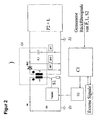
- the first converter stage P1 and the first potential separation G1 is performed integrated. More specifically, in this embodiment, it is designed as a forward converter, in which therefore a transformer with windings N1, N2 is clocked on the primary side via the switch S1. The two windings N1 and N2 are wound in the same direction, so that the transmission of energy always takes place when the switch S1 is activated by the digitally integrated control unit C1 via the potential separation stage G2.
- the mains voltage is applied, which is designated U in and is converted on the output side into a voltage U out .
- a diode Via a diode is a current I FLB2 , which charges an energy storage element K1, at which sets a voltage U K1 .
- This energy storage element K1 may be, for example, a capacitor or a battery.
- a stabilized intermediate voltage U K1 arises at the energy storage element K1 , starting from which the second converter stage P2 and the lighting means L can be fed.
- the digitally integrated control unit C1 can be designed to receive external signals or, for example, to output signals via a connected bus line.
- These signals may, for example, be commands (such as on or off commands or dimming value specifications) or status information (in particular the information regarding a mains voltage failure in the case of application of the invention to emergency lighting).
- the digitally integrated control unit C1 may receive feedback signals from the second converter stage P2, are returned from the light source L or the switch S2 of the second converter P2. This can be done without potential isolation, since the digitally integrated control unit C1 according to the embodiment of FIG. 2 with respect to the mains voltage side is disconnected via the potential separation element G2.
- the resonant discontinuous operation of the forward converter allows a significant reduction of the switching losses and thus also a reduction of the required components.
- a capacitance K2 is arranged on the primary side of the forward converter in parallel or else in series with the coil N1, by appropriate selection of the switching frequency, a reversal between the coil N1 and the capacitor K2 can be achieved. If this swinging is in the range of the switching frequency of the control of the switch S1, then this can always be turned on when just the voltage across the switch S1 has a low value. Then the power loss due to the switching is minimized at the moment of switching.
- the switching frequency can be selected so that when operating the forward converter with rated power such a resonant and thus loss-optimized operation can be achieved.
- a resonance element corresponding to the capacitance K2 which enables resonant operation by utilizing a resonant circuit in conjunction with the coil N1
- FIG. 3 shows a modification of the embodiment of FIG. 2 in that the forward converter is now designed for continuous mode.
- a third winding M3 is essentially provided on the primary side, to which a diode is connected in series, and wherein the winding of the third coil N3 is in the opposite direction to the first coil N1 and N2.
- This coil N3 serves to reduce the magnetization of the primary-side coil N1.
- a possible extension of the forward converter according to the embodiment according to Fig. 3 is the addition of a smoothing reactor after the diode which carries the current I FLB2 and another diode whose cathode is connected between this diode (D_IFLB2) and the smoothing reactor and its anode at the end of the coil N2 which is not connected to the diode ( D_IFLB2) is connected.
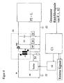
- FIG. 4 shows a further embodiment that differs from the embodiments of FIG. 2 and FIG. 3 differs in that the first converter stage P1 is formed together with the potential separation G1 as a flyback converter (flyback converter).
- a transformer with windings N1 and N2 is provided, which is clocked on the primary side via the switch S1, which in turn is electrically isolated by the potential separation G2 of the digitally integrated Control unit C1 is driven off.
- the flyback converter it is provided in the flyback converter that the windings N1 and N2 are wound in opposite directions.
- the flyback converter then transfers power to the secondary side when the switch S1 is open, driven by the digitally integrated control unit C1.
- FIG. 5 now shows in detail a possible embodiment of the second converter stage, wherein this second converter stage P2 according to FIG. 5 with each implementation of the first converter stage P1 with potential separation G1 according to the figures Fig. 2 .
- Fig. 3 or Fig. 4 can be combined.
- a light source L at which a voltage U L drops and is traversed by a current I L , is supplied from the stabilized intermediate voltage to the energy storage element K1.
- the digitally integrated control unit C1 controls the switch S2 of the second converter stage P2, which is connected in series with an inductance L p2 .
- the voltage across the energy storage element K1 can thus be increased or decreased in a relatively large range to a voltage suitable for the operation of the light source L.
- FIG. 6 Now shows an embodiment, which differs from the embodiment according to the implementation of FIG. 2 to FIG. 5 fundamentally different in that now the digitally integrated control unit C1 not disconnected from the mains voltage side, ie in this case the primary side integrated potential separation / converter circuit P / G1.
- the digitally integrated control unit C1 controls the first converter stage P1 and more precisely, in this example, a switch S1 in series with the primary-side winding N1 of the forward converter.
- Fig. 6 is also suitable for a resonant discontinuous operation of the forward converter. If a capacitance K2 is arranged on the primary side of the forward converter in parallel or else in series with the coil N1, by appropriate selection of the switching frequency, a reversal between the coil N1 and the capacitor K2 can be achieved.
- the use of the capacity K2 can also be done for a further purpose.
- the resonant circuit is formed by the transformer inductances as well as switching capacities and / or stray capacitances.
- the switching of the electronic switch element should take place precisely when the oscillations pass through zero to have. For this it is necessary to influence the frequency of these vibrations. This is achieved by introducing additional capacity, such as the capacity K2. With appropriate dimensioning of this capacity K2 then the switching takes place exactly at the zero crossing or in the vicinity of the zero crossing.
- the voltage across the switch S1 is measured and supplied to the control circuit C1. By recognizing the switch-on, the operating frequency results.
- the output voltage (or the transmitted energy) is determined by the duty cycle of the PWM switching signal.
- the monitoring of the voltage across the switch S1 and the current through the switch S1 can be used to detect whether a resonant operation and thus a normal operating state is present or an error case, for example, an overload or a lack of load ("no load" ).
- an error case for example, an overload or a lack of load ("no load" ).
- the connected load no longer corresponds to the rated power.
- the demagnetization of the coil N1 no longer occurs at the given time, but prematurely or else delayed or does not occur.
- an error case can be detected. Due to the digital implementation of the control unit C1, a discrete sampling of the return signals and thus of the voltage across the switch S1 can take place at several times during a switching cycle.
- the feedback parameters can be stored in the memory register and the time course for the detection of the presence of an error case can be evaluated by the logic circuit.
- the duration of the switch-on time determines the level of the transmitted energy and thus the output voltage.
- the logic circuit can also be determined by evaluating the time course during the previous switching cycles necessary for the activation of the switch S1 duty cycle and transmitted to the PWM (pulse width modulation) driver.
- the forward converter can also assume the function of an active (ie provided with a controlled switch) power factor correction circuit (PFC).
- PFC power factor correction circuit
- This function of the power factor correction circuit (PFC) for example, by a discontinuous operation of the forward converter at a very low duty cycle or even by a continuous operation of the forward converter when placing the capacitance K2 on the secondary side parallel to the secondary diode (freewheeling diode) can be achieved.
- the control unit C1 detects the input voltage U in as a feedback signal
- the duty ratio of the switch S1 can be controlled so that the current absorbed by the coil N1 on average follows the course of the sinusoidal input voltage Uin.
- the digital integrated control unit C1 is the primary side not isolated from the mains voltage, is preferably as in FIG. 7 shown driving the second converter stage P2, and in the illustrated case of the switch S2 of the second potential converter stage P2, starting from the digitally integrated control circuit C1 via a potential separation element G2 executed.
- a flyback converter with windings 2, 6 for charging a battery 13 is coupled to a forward converter (windings 2, 7) for operating an LED 14.
- the LED 14 can also be operated via a second switching stage (by means of the switch S2) starting from the battery 13 when no mains voltage is applied.
- the primary-side switching stage P1 is formed by the primary winding 2 and the freewheeling winding 15 with the freewheeling diode 16 and the optional current shunt 5.
- the switch S1 the power consumption is controlled by P1.
- the switch S1 is driven via a potential-separating member G2 through the IC C1.
- the optional power shunt 5 can either via a potential-separated path G2 'transmit a feedback or error signal to the IC C1 or disable directly via a direct shutdown the switch S1 in case of error.
- the transformer with its primary winding 2, the free-wheeling winding 15 and the secondary windings 6 and 7 forms the potential-separating member G1.
- the capacitors 10 and 11 and the rechargeable battery 13 form the energy storage K1.
- the switching stage P2 is formed from the secondary sides 6, 7 of the transformer and the rechargeable battery 13 subsequent buck-boost converter with the switch S2.
- the switching stage P2 can also be formed by, for example, a buck converter or by a boost converter.
- the rechargeable battery 13 subsequent buck-boost converter is driven by the switch S2 and formed by the throttle 21 and the freewheeling diode 22.
- the reactor 21 is magnetized.
- the reactor 21 drives the current through the diode 22, the LED 14 via the return path (about 6 and 8) on. Due to the charge of the capacitor 10 and the voltage conditions, a current can flow through the LED 14 during the charging phase (S2 switched on).
- the charging circuit for the rechargeable battery 13 is formed by the secondary side 6 and the diode 8 and a smoothing capacitor 11. Based on the voltage divider 12, the IC C1 to the charging voltage and also to close the voltage at the primary side of the transformer and thus to the mains voltage.
- the LED operating circuit for the mains operation is formed by the secondary side 7 and the diode 9 and 18, a smoothing choke 20 and a smoothing capacitor 10, which form the secondary side of a forward converter.
- the coil 20 is possible to arrange the coil 20 on the common core of the transformer of the combined forward and flyback converter. Since an emergency light operation is required only in the case when no mains voltage is applied, there may be no influence of the flyback or forward converter when operating the coil 20 in emergency lighting mode. By appropriate arrangement of the windings on different core legs of the shared ferrite core, an influence of the windings can be further reduced to a minimum.
- the individual windings can be arranged on the common core, that the transformer windings 2, 7, 6 are decoupled against the choke winding 21 and vice versa.
- the transformer windings 2, 7, 6 and the choke winding 21 can be mounted on the common core and distributed so that the magnetic fluxes generated by the choke winding 21 induce opposing currents in the transformer windings 2, 7, 6 and that of the transformer windings 2 , 7, 6 are magnetic fluxes that run past the inductor winding and do not induce current therein.
- a so-called E-core can be used as the design.
- the common core may consist of two outer and one a middle leg and these three legs at both ends bridging yoke parts are that the choke winding 21 are arranged distributed in half and co-wound on different legs of the common core, that the transformer windings 2, 7, 6 on the third core are arranged, and that the third leg is provided with an air gap.
- the combination of forward converter and flyback converter allows independent control of the two secondary sides. While the transmitted power of the flyback converter is highly dependent on the switch-on ratio of the switch S1, a constant power can be transmitted through appropriate design of the forward converter (i.e., selection of the core of the transformer) over a wide range of turn-on ratios. Thus, there is a possibility that the rechargeable battery 13 is recharged according to its charging curve, while the LED (s) 14 is operated evenly (thus equal brightness is achieved).
- the assignment of the forward converter and the flyback converter can also be interchanged.
- control unit C1 can be arranged on the primary side (ie not be galvanically decoupled with respect to the primary side) and the switch S2 can be activated by a galvanic isolation.
- the regulation of the two power converter stages P1 and P2 can be done by detecting Return signals occur on the primary side, for example by detecting the voltage across the switch S1 and the current through the switch S1.
- the control unit C1 can be closed-loop control on the basis of feedback signals detected on the primary side.
- the switch S2 is clocked by the control unit C1 via a galvanic isolation and thus operated the light source via the power converter stage P2.
- the power converter stage P2 is formed only by the secondary side elements of the forward converter for operating the LED.
- a return of feedback signals can be done via a potential-separated transmission in the power converter stage P2 or on the light source and the control unit C1 are supplied.
- a typical application of such a converter is an emergency lighting with LED, for example, for so-called.
- "EXIT" sign (escape route display) or the escape route lighting.
- control unit C1 electrically isolated controls a combined converter stage P1, on the one hand an energy storage and on the other hand, in parallel, the bulbs provided.
- a second converter stage with the switch S2 (which is not electrically isolated by the control unit C1) can then selectively supply the lighting means 14.
Landscapes
- Circuit Arrangement For Electric Light Sources In General (AREA)
- Dc-Dc Converters (AREA)
Applications Claiming Priority (3)
| Application Number | Priority Date | Filing Date | Title |
|---|---|---|---|
| DE102007027551 | 2007-06-15 | ||
| EP08773407A EP2158794B1 (fr) | 2007-06-15 | 2008-06-12 | Appareil permettant de faire fonctionner une source de lumière, notamment une del |
| PCT/EP2008/004727 WO2008151800A1 (fr) | 2007-06-15 | 2008-06-12 | Appareil permettant de faire fonctionner une source de lumière, notamment une del |
Related Parent Applications (2)
| Application Number | Title | Priority Date | Filing Date |
|---|---|---|---|
| EP08773407A Division EP2158794B1 (fr) | 2007-06-15 | 2008-06-12 | Appareil permettant de faire fonctionner une source de lumière, notamment une del |
| EP08773407.5 Division | 2008-06-12 |
Publications (3)
| Publication Number | Publication Date |
|---|---|
| EP2341761A2 true EP2341761A2 (fr) | 2011-07-06 |
| EP2341761A3 EP2341761A3 (fr) | 2012-09-26 |
| EP2341761B1 EP2341761B1 (fr) | 2022-12-14 |
Family
ID=39683449
Family Applications (3)
| Application Number | Title | Priority Date | Filing Date |
|---|---|---|---|
| EP11155583.5A Active EP2341761B1 (fr) | 2007-06-15 | 2008-06-12 | Appareil pour opérer une source lumineuse, notamment une DEL |
| EP10169261.4A Active EP2247162B1 (fr) | 2007-06-15 | 2008-06-12 | Appareil pour opérer une source lumineuse, notamment une DEL |
| EP08773407A Active EP2158794B1 (fr) | 2007-06-15 | 2008-06-12 | Appareil permettant de faire fonctionner une source de lumière, notamment une del |
Family Applications After (2)
| Application Number | Title | Priority Date | Filing Date |
|---|---|---|---|
| EP10169261.4A Active EP2247162B1 (fr) | 2007-06-15 | 2008-06-12 | Appareil pour opérer une source lumineuse, notamment une DEL |
| EP08773407A Active EP2158794B1 (fr) | 2007-06-15 | 2008-06-12 | Appareil permettant de faire fonctionner une source de lumière, notamment une del |
Country Status (6)
| Country | Link |
|---|---|
| US (1) | US8384302B2 (fr) |
| EP (3) | EP2341761B1 (fr) |
| CN (1) | CN101715655B (fr) |
| AT (2) | AT515913B1 (fr) |
| DE (1) | DE112008001505B4 (fr) |
| WO (1) | WO2008151800A1 (fr) |
Families Citing this family (22)
| Publication number | Priority date | Publication date | Assignee | Title |
|---|---|---|---|---|
| DE102008055862A1 (de) * | 2008-11-05 | 2010-05-06 | Tridonicatco Gmbh & Co. Kg | Leuchtmittel-Betriebsgerät mit Potentialtrennung |
| EP2425681B1 (fr) * | 2009-04-03 | 2017-07-19 | Tridonic GmbH & Co KG | Circuit de pilotage pour un del |
| EP2420108B1 (fr) * | 2009-04-03 | 2020-07-15 | Tridonic GmbH & Co KG | Circuit de commande pour leds |
| AT508969B1 (de) * | 2009-10-22 | 2011-07-15 | Lunatone Ind Elektronik Gmbh | Led-stromversorgung |
| DE102009044593B4 (de) * | 2009-11-19 | 2018-07-12 | Vossloh-Schwabe Deutschland Gmbh | Betriebssteuergerät zum Betreiben eines Leuchtmittels |
| DE102010003799A1 (de) * | 2010-04-09 | 2011-12-15 | Tridonic Ag | Modulares LED-Beleuchtungssystem mit Notlichtfunktion |
| DE102010003797A1 (de) | 2010-04-09 | 2011-10-13 | Tridonic Ag | Modulares LED-Beleuchtungssystem mit Notlichtfunktion |
| JP6072776B2 (ja) * | 2011-05-18 | 2017-02-01 | フィリップス ライティング ホールディング ビー ヴィ | Ledレトロフィット駆動回路及びledレトロフィット駆動回路を動作させる方法 |
| CN102264181A (zh) * | 2011-07-11 | 2011-11-30 | 苏州辰戈电子有限公司 | 一种多路led控制与驱动系统 |
| DE102012007449B4 (de) * | 2012-04-13 | 2024-02-22 | Tridonic Gmbh & Co Kg | Verfahren zum Betreiben eines LLC-Resonanzwandlers für ein Leuchtmittel, Wandler und LED-Konverter |
| EP2675037A1 (fr) * | 2012-06-12 | 2013-12-18 | Vossloh-Schwabe Deutschland GmbH | Dispositif de commande de fonctionnement et procédé de commande de fonctionnement d'un système d'éclairage avec éclairage de secours |
| DE102012214832B4 (de) | 2012-08-21 | 2024-11-28 | Tridonic Uk Ltd. | Notlichtgerät mit Potentialtrennung zwischen Leuchtmittel und Energiespeicher |
| DE102012215481A1 (de) * | 2012-08-31 | 2014-03-06 | Tridonic Gmbh & Co Kg | Betriebsgerät zur Ansteuerung einer LED-Strecke mit sekundärseitiger Steuereinheit |
| AT14948U1 (de) * | 2013-12-03 | 2016-09-15 | Tridonic Gmbh & Co Kg | Treiberschaltung für Leuchtmittel insbesondere LEDs |
| DE102013224749B4 (de) * | 2013-12-03 | 2025-01-23 | Tridonic Gmbh & Co Kg | Treiberschaltung für Leuchtmittel, insbesondere LEDs, LED-Modul und Leuchte, jeweils mit einer solchen Schaltung, sowie entsprechendes Verfahren |
| AT15167U1 (de) * | 2014-01-29 | 2017-02-15 | Tridonic Gmbh & Co Kg | Erfassung eines LED-Moduls |
| AT15169U1 (de) * | 2014-01-30 | 2017-02-15 | Tridonic Gmbh & Co Kg | Erfassung eines LED-Moduls |
| US9241380B2 (en) | 2014-03-04 | 2016-01-19 | Osram Sylvania Inc. | Hybrid dimming control techniques for lighting drivers |
| US9491820B2 (en) | 2014-03-04 | 2016-11-08 | Osram Sylvania Inc. | Hybrid dimming control techniques for LED drivers |
| CN105657900B (zh) * | 2016-02-26 | 2018-04-17 | 矽力杰半导体技术(杭州)有限公司 | 调光电路、控制电路和调光方法 |
| US11026311B2 (en) | 2017-06-19 | 2021-06-01 | Abl Ip Holding Llc | Emergency lighting system with power rollback |
| EP4164343A1 (fr) * | 2021-10-08 | 2023-04-12 | Schneider Electric Industries SAS | Circuit de commande d'alimentation, appareil de surveillance, système de surveillance |
Family Cites Families (10)
| Publication number | Priority date | Publication date | Assignee | Title |
|---|---|---|---|---|
| US4988889A (en) * | 1989-07-03 | 1991-01-29 | Self-Powered Lighting, Inc. | Power source for emergency lighting systems |
| US6369529B1 (en) | 2000-06-01 | 2002-04-09 | Tachi-S Engineering, U.S.A. Inc. | Remote power seat control system and method |
| US6369525B1 (en) * | 2000-11-21 | 2002-04-09 | Philips Electronics North America | White light-emitting-diode lamp driver based on multiple output converter with output current mode control |
| US6504267B1 (en) * | 2001-12-14 | 2003-01-07 | Koninklijke Philips Electronics N.V. | Flyback power converter with secondary-side control and primary-side soft switching |
| AU2003210890A1 (en) | 2002-02-06 | 2003-09-02 | Color Kinetics Incorporated | Controlled lighting methods and apparatus |
| US7459864B2 (en) | 2004-03-15 | 2008-12-02 | Philips Solid-State Lighting Solutions, Inc. | Power control methods and apparatus |
| EP1608206B1 (fr) | 2004-06-14 | 2009-08-12 | STMicroelectronics S.r.l. | Dispositif d'alimentation de diodes é électroluminescentes avec intensité variable de la lumière |
| US7142140B2 (en) * | 2004-07-27 | 2006-11-28 | Silicon Laboratories Inc. | Auto scanning ADC for DPWM |
| US7256556B2 (en) | 2004-09-28 | 2007-08-14 | Acuity Brands, Inc. | Equipment and methods for emergency lighting that provides brownout detection and protection |
| US7336059B2 (en) * | 2005-11-15 | 2008-02-26 | General Electric Company | System and method for charging and discharging a superconducting coil |
-
2008
- 2008-06-12 AT ATA9194/2008A patent/AT515913B1/de not_active IP Right Cessation
- 2008-06-12 EP EP11155583.5A patent/EP2341761B1/fr active Active
- 2008-06-12 WO PCT/EP2008/004727 patent/WO2008151800A1/fr not_active Ceased
- 2008-06-12 AT AT08773407T patent/ATE539591T1/de active
- 2008-06-12 CN CN2008800203831A patent/CN101715655B/zh not_active Expired - Fee Related
- 2008-06-12 DE DE112008001505.8T patent/DE112008001505B4/de active Active
- 2008-06-12 EP EP10169261.4A patent/EP2247162B1/fr active Active
- 2008-06-12 EP EP08773407A patent/EP2158794B1/fr active Active
- 2008-06-12 US US12/664,346 patent/US8384302B2/en active Active
Non-Patent Citations (1)
| Title |
|---|
| None |
Also Published As
| Publication number | Publication date |
|---|---|
| US8384302B2 (en) | 2013-02-26 |
| EP2247162B1 (fr) | 2016-01-06 |
| EP2158794B1 (fr) | 2011-12-28 |
| EP2158794A1 (fr) | 2010-03-03 |
| CN101715655B (zh) | 2012-04-25 |
| DE112008001505B4 (de) | 2022-09-29 |
| WO2008151800A1 (fr) | 2008-12-18 |
| ATE539591T1 (de) | 2012-01-15 |
| EP2341761B1 (fr) | 2022-12-14 |
| AT515913B1 (de) | 2016-01-15 |
| AT515913A5 (de) | 2016-01-15 |
| EP2247162A1 (fr) | 2010-11-03 |
| US20100301766A1 (en) | 2010-12-02 |
| EP2341761A3 (fr) | 2012-09-26 |
| CN101715655A (zh) | 2010-05-26 |
| DE112008001505A5 (de) | 2010-05-12 |
Similar Documents
| Publication | Publication Date | Title |
|---|---|---|
| EP2341761B1 (fr) | Appareil pour opérer une source lumineuse, notamment une DEL | |
| DE112009002526B4 (de) | Leuchtmittel-Betriebsgerät mit Potentialtrennung, LED-Lampe, Leuchte und integrierte Steuereinheit | |
| EP2556726B1 (fr) | Système d'éclairage à del modulaire, à fonction d'éclairage d'urgence | |
| DE102013111348B4 (de) | Verfahren und Schaltungsanordnung zum Ermitteln einer Entmagnetisierungsnullstromzeit | |
| EP2888800B1 (fr) | Appareil de lumière de secours | |
| EP2548408B1 (fr) | Système d'éclairage à led avec un mémoire pour stocker des donnés opérationelles | |
| AT512780B1 (de) | Schaltnetzteil sowie Wechselrichter und Strangüberwachung mit einem solchen Schaltnetzteil | |
| EP3078242B1 (fr) | Circuit d'excitation pour moyen d'éclairage, en particulier des diodes électroluminescentes | |
| DE112012001746T5 (de) | Energie-Umwandlungsvorrichtung und mit einer solchen ausgestattete Stromversorgungsvorrichtung in einem Fahrzeug | |
| DE102013111675A1 (de) | Verfahren und steuerung zum ermitteln einer entmagnetisierungsnullstromzeit für ein schaltnetzteil | |
| DE112012005944T5 (de) | DC/DC-Wandler, Onboard-Einheit und Ladevorrichtung | |
| WO2011124721A1 (fr) | Système d'éclairage del modulaire à fonction de lumière de secours | |
| DE112009001632T5 (de) | Spannungswandler | |
| EP2425680B1 (fr) | Circuit pour faire fonctionner des diodes luminescentes | |
| EP1867035B1 (fr) | Procède de fonctionnement d'une alimentation a découpage avec récupération d'énergie de diffusion cote primaire | |
| DE102009044593A1 (de) | Betriebssteuergerät zum Betreiben eines Leuchtmittels | |
| EP2719065B1 (fr) | Procédé de connexion d'un circuit convertisseur à transfert indirect cadencé, et circuit convertisseur à transfert indirect | |
| DE102009021048A1 (de) | Schaltung zum Beheizen wenigstens einer Heizwendel einer Gasentladungslampe, und Beleuchtungssystem | |
| DE202016102125U1 (de) | Stromumwandlungssystem | |
| EP3295771B1 (fr) | Dispositif à convertisseur cadencé pour faire fonctionner des dispositifs d'éclairage | |
| AT16193U1 (de) | Vorrichtung mit getaktetem Wandler zum Betrieb von Leuchtmitteln | |
| DE212014000115U1 (de) | Betriebsschaltung für Leuchtdioden mit Filterelement | |
| DE102013106229A1 (de) | Wandler |
Legal Events
| Date | Code | Title | Description |
|---|---|---|---|
| PUAI | Public reference made under article 153(3) epc to a published international application that has entered the european phase |
Free format text: ORIGINAL CODE: 0009012 |
|
| AC | Divisional application: reference to earlier application |
Ref document number: 2158794 Country of ref document: EP Kind code of ref document: P |
|
| AK | Designated contracting states |
Kind code of ref document: A2 Designated state(s): AT BE BG CH CY CZ DE DK EE ES FI FR GB GR HR HU IE IS IT LI LT LU LV MC MT NL NO PL PT RO SE SI SK TR |
|
| PUAL | Search report despatched |
Free format text: ORIGINAL CODE: 0009013 |
|
| AK | Designated contracting states |
Kind code of ref document: A3 Designated state(s): AT BE BG CH CY CZ DE DK EE ES FI FR GB GR HR HU IE IS IT LI LT LU LV MC MT NL NO PL PT RO SE SI SK TR |
|
| RIC1 | Information provided on ipc code assigned before grant |
Ipc: H05B 33/08 20060101AFI20120817BHEP |
|
| 17P | Request for examination filed |
Effective date: 20130326 |
|
| 17Q | First examination report despatched |
Effective date: 20140826 |
|
| STAA | Information on the status of an ep patent application or granted ep patent |
Free format text: STATUS: EXAMINATION IS IN PROGRESS |
|
| APBK | Appeal reference recorded |
Free format text: ORIGINAL CODE: EPIDOSNREFNE |
|
| APBN | Date of receipt of notice of appeal recorded |
Free format text: ORIGINAL CODE: EPIDOSNNOA2E |
|
| APBR | Date of receipt of statement of grounds of appeal recorded |
Free format text: ORIGINAL CODE: EPIDOSNNOA3E |
|
| APAF | Appeal reference modified |
Free format text: ORIGINAL CODE: EPIDOSCREFNE |
|
| APAF | Appeal reference modified |
Free format text: ORIGINAL CODE: EPIDOSCREFNE |
|
| APBT | Appeal procedure closed |
Free format text: ORIGINAL CODE: EPIDOSNNOA9E |
|
| REG | Reference to a national code |
Ref country code: DE Ref legal event code: R079 Ref document number: 502008017260 Country of ref document: DE Free format text: PREVIOUS MAIN CLASS: H05B0033080000 Ipc: H05B0045385000 |
|
| RIC1 | Information provided on ipc code assigned before grant |
Ipc: H05B 45/385 20200101AFI20220808BHEP |
|
| GRAP | Despatch of communication of intention to grant a patent |
Free format text: ORIGINAL CODE: EPIDOSNIGR1 |
|
| GRAS | Grant fee paid |
Free format text: ORIGINAL CODE: EPIDOSNIGR3 |
|
| STAA | Information on the status of an ep patent application or granted ep patent |
Free format text: STATUS: GRANT OF PATENT IS INTENDED |
|
| GRAA | (expected) grant |
Free format text: ORIGINAL CODE: 0009210 |
|
| STAA | Information on the status of an ep patent application or granted ep patent |
Free format text: STATUS: THE PATENT HAS BEEN GRANTED |
|
| AC | Divisional application: reference to earlier application |
Ref document number: 2158794 Country of ref document: EP Kind code of ref document: P |
|
| AK | Designated contracting states |
Kind code of ref document: B1 Designated state(s): AT BE BG CH CY CZ DE DK EE ES FI FR GB GR HR HU IE IS IT LI LT LU LV MC MT NL NO PL PT RO SE SI SK TR |
|
| INTG | Intention to grant announced |
Effective date: 20220809 |
|
| REG | Reference to a national code |
Ref country code: GB Ref legal event code: FG4D Free format text: NOT ENGLISH |
|
| REG | Reference to a national code |
Ref country code: CH Ref legal event code: EP |
|
| REG | Reference to a national code |
Ref country code: DE Ref legal event code: R096 Ref document number: 502008017260 Country of ref document: DE |
|
| REG | Reference to a national code |
Ref country code: IE Ref legal event code: FG4D Free format text: LANGUAGE OF EP DOCUMENT: GERMAN |
|
| REG | Reference to a national code |
Ref country code: AT Ref legal event code: REF Ref document number: 1538433 Country of ref document: AT Kind code of ref document: T Effective date: 20230115 |
|
| REG | Reference to a national code |
Ref country code: LT Ref legal event code: MG9D |
|
| REG | Reference to a national code |
Ref country code: NL Ref legal event code: MP Effective date: 20221214 |
|
| PG25 | Lapsed in a contracting state [announced via postgrant information from national office to epo] |
Ref country code: SE Free format text: LAPSE BECAUSE OF FAILURE TO SUBMIT A TRANSLATION OF THE DESCRIPTION OR TO PAY THE FEE WITHIN THE PRESCRIBED TIME-LIMIT Effective date: 20221214 Ref country code: NO Free format text: LAPSE BECAUSE OF FAILURE TO SUBMIT A TRANSLATION OF THE DESCRIPTION OR TO PAY THE FEE WITHIN THE PRESCRIBED TIME-LIMIT Effective date: 20230314 Ref country code: LT Free format text: LAPSE BECAUSE OF FAILURE TO SUBMIT A TRANSLATION OF THE DESCRIPTION OR TO PAY THE FEE WITHIN THE PRESCRIBED TIME-LIMIT Effective date: 20221214 Ref country code: FI Free format text: LAPSE BECAUSE OF FAILURE TO SUBMIT A TRANSLATION OF THE DESCRIPTION OR TO PAY THE FEE WITHIN THE PRESCRIBED TIME-LIMIT Effective date: 20221214 |
|
| REG | Reference to a national code |
Ref country code: DE Ref legal event code: R084 Ref document number: 502008017260 Country of ref document: DE |
|
| PG25 | Lapsed in a contracting state [announced via postgrant information from national office to epo] |
Ref country code: LV Free format text: LAPSE BECAUSE OF FAILURE TO SUBMIT A TRANSLATION OF THE DESCRIPTION OR TO PAY THE FEE WITHIN THE PRESCRIBED TIME-LIMIT Effective date: 20221214 Ref country code: HR Free format text: LAPSE BECAUSE OF FAILURE TO SUBMIT A TRANSLATION OF THE DESCRIPTION OR TO PAY THE FEE WITHIN THE PRESCRIBED TIME-LIMIT Effective date: 20221214 Ref country code: GR Free format text: LAPSE BECAUSE OF FAILURE TO SUBMIT A TRANSLATION OF THE DESCRIPTION OR TO PAY THE FEE WITHIN THE PRESCRIBED TIME-LIMIT Effective date: 20230315 |
|
| PG25 | Lapsed in a contracting state [announced via postgrant information from national office to epo] |
Ref country code: NL Free format text: LAPSE BECAUSE OF FAILURE TO SUBMIT A TRANSLATION OF THE DESCRIPTION OR TO PAY THE FEE WITHIN THE PRESCRIBED TIME-LIMIT Effective date: 20221214 |
|
| P01 | Opt-out of the competence of the unified patent court (upc) registered |
Effective date: 20230530 |
|
| PG25 | Lapsed in a contracting state [announced via postgrant information from national office to epo] |
Ref country code: RO Free format text: LAPSE BECAUSE OF FAILURE TO SUBMIT A TRANSLATION OF THE DESCRIPTION OR TO PAY THE FEE WITHIN THE PRESCRIBED TIME-LIMIT Effective date: 20221214 Ref country code: PT Free format text: LAPSE BECAUSE OF FAILURE TO SUBMIT A TRANSLATION OF THE DESCRIPTION OR TO PAY THE FEE WITHIN THE PRESCRIBED TIME-LIMIT Effective date: 20230414 Ref country code: ES Free format text: LAPSE BECAUSE OF FAILURE TO SUBMIT A TRANSLATION OF THE DESCRIPTION OR TO PAY THE FEE WITHIN THE PRESCRIBED TIME-LIMIT Effective date: 20221214 Ref country code: EE Free format text: LAPSE BECAUSE OF FAILURE TO SUBMIT A TRANSLATION OF THE DESCRIPTION OR TO PAY THE FEE WITHIN THE PRESCRIBED TIME-LIMIT Effective date: 20221214 Ref country code: CZ Free format text: LAPSE BECAUSE OF FAILURE TO SUBMIT A TRANSLATION OF THE DESCRIPTION OR TO PAY THE FEE WITHIN THE PRESCRIBED TIME-LIMIT Effective date: 20221214 |
|
| PG25 | Lapsed in a contracting state [announced via postgrant information from national office to epo] |
Ref country code: SK Free format text: LAPSE BECAUSE OF FAILURE TO SUBMIT A TRANSLATION OF THE DESCRIPTION OR TO PAY THE FEE WITHIN THE PRESCRIBED TIME-LIMIT Effective date: 20221214 Ref country code: PL Free format text: LAPSE BECAUSE OF FAILURE TO SUBMIT A TRANSLATION OF THE DESCRIPTION OR TO PAY THE FEE WITHIN THE PRESCRIBED TIME-LIMIT Effective date: 20221214 Ref country code: IS Free format text: LAPSE BECAUSE OF FAILURE TO SUBMIT A TRANSLATION OF THE DESCRIPTION OR TO PAY THE FEE WITHIN THE PRESCRIBED TIME-LIMIT Effective date: 20230414 |
|
| REG | Reference to a national code |
Ref country code: DE Ref legal event code: R097 Ref document number: 502008017260 Country of ref document: DE |
|
| PLBE | No opposition filed within time limit |
Free format text: ORIGINAL CODE: 0009261 |
|
| STAA | Information on the status of an ep patent application or granted ep patent |
Free format text: STATUS: NO OPPOSITION FILED WITHIN TIME LIMIT |
|
| PG25 | Lapsed in a contracting state [announced via postgrant information from national office to epo] |
Ref country code: DK Free format text: LAPSE BECAUSE OF FAILURE TO SUBMIT A TRANSLATION OF THE DESCRIPTION OR TO PAY THE FEE WITHIN THE PRESCRIBED TIME-LIMIT Effective date: 20221214 |
|
| 26N | No opposition filed |
Effective date: 20230915 |
|
| PG25 | Lapsed in a contracting state [announced via postgrant information from national office to epo] |
Ref country code: SI Free format text: LAPSE BECAUSE OF FAILURE TO SUBMIT A TRANSLATION OF THE DESCRIPTION OR TO PAY THE FEE WITHIN THE PRESCRIBED TIME-LIMIT Effective date: 20221214 |
|
| PG25 | Lapsed in a contracting state [announced via postgrant information from national office to epo] |
Ref country code: MC Free format text: LAPSE BECAUSE OF FAILURE TO SUBMIT A TRANSLATION OF THE DESCRIPTION OR TO PAY THE FEE WITHIN THE PRESCRIBED TIME-LIMIT Effective date: 20221214 |
|
| PG25 | Lapsed in a contracting state [announced via postgrant information from national office to epo] |
Ref country code: MC Free format text: LAPSE BECAUSE OF FAILURE TO SUBMIT A TRANSLATION OF THE DESCRIPTION OR TO PAY THE FEE WITHIN THE PRESCRIBED TIME-LIMIT Effective date: 20221214 |
|
| REG | Reference to a national code |
Ref country code: CH Ref legal event code: PL |
|
| REG | Reference to a national code |
Ref country code: BE Ref legal event code: MM Effective date: 20230630 |
|
| PG25 | Lapsed in a contracting state [announced via postgrant information from national office to epo] |
Ref country code: LU Free format text: LAPSE BECAUSE OF NON-PAYMENT OF DUE FEES Effective date: 20230612 |
|
| REG | Reference to a national code |
Ref country code: IE Ref legal event code: MM4A |
|
| PG25 | Lapsed in a contracting state [announced via postgrant information from national office to epo] |
Ref country code: LU Free format text: LAPSE BECAUSE OF NON-PAYMENT OF DUE FEES Effective date: 20230612 |
|
| PG25 | Lapsed in a contracting state [announced via postgrant information from national office to epo] |
Ref country code: IE Free format text: LAPSE BECAUSE OF NON-PAYMENT OF DUE FEES Effective date: 20230612 |
|
| PG25 | Lapsed in a contracting state [announced via postgrant information from national office to epo] |
Ref country code: IE Free format text: LAPSE BECAUSE OF NON-PAYMENT OF DUE FEES Effective date: 20230612 Ref country code: CH Free format text: LAPSE BECAUSE OF NON-PAYMENT OF DUE FEES Effective date: 20230630 |
|
| PG25 | Lapsed in a contracting state [announced via postgrant information from national office to epo] |
Ref country code: IT Free format text: LAPSE BECAUSE OF FAILURE TO SUBMIT A TRANSLATION OF THE DESCRIPTION OR TO PAY THE FEE WITHIN THE PRESCRIBED TIME-LIMIT Effective date: 20221214 Ref country code: BE Free format text: LAPSE BECAUSE OF NON-PAYMENT OF DUE FEES Effective date: 20230630 |
|
| REG | Reference to a national code |
Ref country code: AT Ref legal event code: MM01 Ref document number: 1538433 Country of ref document: AT Kind code of ref document: T Effective date: 20230612 |
|
| PG25 | Lapsed in a contracting state [announced via postgrant information from national office to epo] |
Ref country code: AT Free format text: LAPSE BECAUSE OF NON-PAYMENT OF DUE FEES Effective date: 20230612 |
|
| PG25 | Lapsed in a contracting state [announced via postgrant information from national office to epo] |
Ref country code: AT Free format text: LAPSE BECAUSE OF NON-PAYMENT OF DUE FEES Effective date: 20230612 |
|
| PG25 | Lapsed in a contracting state [announced via postgrant information from national office to epo] |
Ref country code: BG Free format text: LAPSE BECAUSE OF FAILURE TO SUBMIT A TRANSLATION OF THE DESCRIPTION OR TO PAY THE FEE WITHIN THE PRESCRIBED TIME-LIMIT Effective date: 20221214 |
|
| PG25 | Lapsed in a contracting state [announced via postgrant information from national office to epo] |
Ref country code: BG Free format text: LAPSE BECAUSE OF FAILURE TO SUBMIT A TRANSLATION OF THE DESCRIPTION OR TO PAY THE FEE WITHIN THE PRESCRIBED TIME-LIMIT Effective date: 20221214 |
|
| PGFP | Annual fee paid to national office [announced via postgrant information from national office to epo] |
Ref country code: DE Payment date: 20250626 Year of fee payment: 18 |
|
| PGFP | Annual fee paid to national office [announced via postgrant information from national office to epo] |
Ref country code: GB Payment date: 20250617 Year of fee payment: 18 |
|
| PGFP | Annual fee paid to national office [announced via postgrant information from national office to epo] |
Ref country code: FR Payment date: 20250624 Year of fee payment: 18 |
|
| PG25 | Lapsed in a contracting state [announced via postgrant information from national office to epo] |
Ref country code: CY Free format text: LAPSE BECAUSE OF FAILURE TO SUBMIT A TRANSLATION OF THE DESCRIPTION OR TO PAY THE FEE WITHIN THE PRESCRIBED TIME-LIMIT; INVALID AB INITIO Effective date: 20080612 |
|
| PG25 | Lapsed in a contracting state [announced via postgrant information from national office to epo] |
Ref country code: HU Free format text: LAPSE BECAUSE OF FAILURE TO SUBMIT A TRANSLATION OF THE DESCRIPTION OR TO PAY THE FEE WITHIN THE PRESCRIBED TIME-LIMIT; INVALID AB INITIO Effective date: 20080612 |
|
| PG25 | Lapsed in a contracting state [announced via postgrant information from national office to epo] |
Ref country code: TR Free format text: LAPSE BECAUSE OF FAILURE TO SUBMIT A TRANSLATION OF THE DESCRIPTION OR TO PAY THE FEE WITHIN THE PRESCRIBED TIME-LIMIT Effective date: 20221214 |