EP2345023B1 - Anzeigeanordnung mit kompensation von schwankungen der pixeltransistormobilität - Google Patents
Anzeigeanordnung mit kompensation von schwankungen der pixeltransistormobilität Download PDFInfo
- Publication number
- EP2345023B1 EP2345023B1 EP09789397A EP09789397A EP2345023B1 EP 2345023 B1 EP2345023 B1 EP 2345023B1 EP 09789397 A EP09789397 A EP 09789397A EP 09789397 A EP09789397 A EP 09789397A EP 2345023 B1 EP2345023 B1 EP 2345023B1
- Authority
- EP
- European Patent Office
- Prior art keywords
- transistor
- reset
- light emission
- line
- emission control
- Prior art date
- Legal status (The legal status is an assumption and is not a legal conclusion. Google has not performed a legal analysis and makes no representation as to the accuracy of the status listed.)
- Active
Links
Images


Classifications
-
- G—PHYSICS
- G09—EDUCATION; CRYPTOGRAPHY; DISPLAY; ADVERTISING; SEALS
- G09G—ARRANGEMENTS OR CIRCUITS FOR CONTROL OF INDICATING DEVICES USING STATIC MEANS TO PRESENT VARIABLE INFORMATION
- G09G3/00—Control arrangements or circuits, of interest only in connection with visual indicators other than cathode-ray tubes
- G09G3/20—Control arrangements or circuits, of interest only in connection with visual indicators other than cathode-ray tubes for presentation of an assembly of a number of characters, e.g. a page, by composing the assembly by combination of individual elements arranged in a matrix no fixed position being assigned to or needed to be assigned to the individual characters or partial characters
- G09G3/22—Control arrangements or circuits, of interest only in connection with visual indicators other than cathode-ray tubes for presentation of an assembly of a number of characters, e.g. a page, by composing the assembly by combination of individual elements arranged in a matrix no fixed position being assigned to or needed to be assigned to the individual characters or partial characters using controlled light sources
- G09G3/30—Control arrangements or circuits, of interest only in connection with visual indicators other than cathode-ray tubes for presentation of an assembly of a number of characters, e.g. a page, by composing the assembly by combination of individual elements arranged in a matrix no fixed position being assigned to or needed to be assigned to the individual characters or partial characters using controlled light sources using electroluminescent panels
- G09G3/32—Control arrangements or circuits, of interest only in connection with visual indicators other than cathode-ray tubes for presentation of an assembly of a number of characters, e.g. a page, by composing the assembly by combination of individual elements arranged in a matrix no fixed position being assigned to or needed to be assigned to the individual characters or partial characters using controlled light sources using electroluminescent panels semiconductive, e.g. using light-emitting diodes [LED]
- G09G3/3208—Control arrangements or circuits, of interest only in connection with visual indicators other than cathode-ray tubes for presentation of an assembly of a number of characters, e.g. a page, by composing the assembly by combination of individual elements arranged in a matrix no fixed position being assigned to or needed to be assigned to the individual characters or partial characters using controlled light sources using electroluminescent panels semiconductive, e.g. using light-emitting diodes [LED] organic, e.g. using organic light-emitting diodes [OLED]
- G09G3/3225—Control arrangements or circuits, of interest only in connection with visual indicators other than cathode-ray tubes for presentation of an assembly of a number of characters, e.g. a page, by composing the assembly by combination of individual elements arranged in a matrix no fixed position being assigned to or needed to be assigned to the individual characters or partial characters using controlled light sources using electroluminescent panels semiconductive, e.g. using light-emitting diodes [LED] organic, e.g. using organic light-emitting diodes [OLED] using an active matrix
- G09G3/3233—Control arrangements or circuits, of interest only in connection with visual indicators other than cathode-ray tubes for presentation of an assembly of a number of characters, e.g. a page, by composing the assembly by combination of individual elements arranged in a matrix no fixed position being assigned to or needed to be assigned to the individual characters or partial characters using controlled light sources using electroluminescent panels semiconductive, e.g. using light-emitting diodes [LED] organic, e.g. using organic light-emitting diodes [OLED] using an active matrix with pixel circuitry controlling the current through the light-emitting element
-
- G—PHYSICS
- G09—EDUCATION; CRYPTOGRAPHY; DISPLAY; ADVERTISING; SEALS
- G09G—ARRANGEMENTS OR CIRCUITS FOR CONTROL OF INDICATING DEVICES USING STATIC MEANS TO PRESENT VARIABLE INFORMATION
- G09G2300/00—Aspects of the constitution of display devices
- G09G2300/04—Structural and physical details of display devices
- G09G2300/0404—Matrix technologies
- G09G2300/0417—Special arrangements specific to the use of low carrier mobility technology
-
- G—PHYSICS
- G09—EDUCATION; CRYPTOGRAPHY; DISPLAY; ADVERTISING; SEALS
- G09G—ARRANGEMENTS OR CIRCUITS FOR CONTROL OF INDICATING DEVICES USING STATIC MEANS TO PRESENT VARIABLE INFORMATION
- G09G2300/00—Aspects of the constitution of display devices
- G09G2300/08—Active matrix structure, i.e. with use of active elements, inclusive of non-linear two terminal elements, in the pixels together with light emitting or modulating elements
- G09G2300/0809—Several active elements per pixel in active matrix panels
- G09G2300/0819—Several active elements per pixel in active matrix panels used for counteracting undesired variations, e.g. feedback or autozeroing
-
- G—PHYSICS
- G09—EDUCATION; CRYPTOGRAPHY; DISPLAY; ADVERTISING; SEALS
- G09G—ARRANGEMENTS OR CIRCUITS FOR CONTROL OF INDICATING DEVICES USING STATIC MEANS TO PRESENT VARIABLE INFORMATION
- G09G2300/00—Aspects of the constitution of display devices
- G09G2300/08—Active matrix structure, i.e. with use of active elements, inclusive of non-linear two terminal elements, in the pixels together with light emitting or modulating elements
- G09G2300/0809—Several active elements per pixel in active matrix panels
- G09G2300/0842—Several active elements per pixel in active matrix panels forming a memory circuit, e.g. a dynamic memory with one capacitor
- G09G2300/0852—Several active elements per pixel in active matrix panels forming a memory circuit, e.g. a dynamic memory with one capacitor being a dynamic memory with more than one capacitor
-
- G—PHYSICS
- G09—EDUCATION; CRYPTOGRAPHY; DISPLAY; ADVERTISING; SEALS
- G09G—ARRANGEMENTS OR CIRCUITS FOR CONTROL OF INDICATING DEVICES USING STATIC MEANS TO PRESENT VARIABLE INFORMATION
- G09G2300/00—Aspects of the constitution of display devices
- G09G2300/08—Active matrix structure, i.e. with use of active elements, inclusive of non-linear two terminal elements, in the pixels together with light emitting or modulating elements
- G09G2300/0809—Several active elements per pixel in active matrix panels
- G09G2300/0842—Several active elements per pixel in active matrix panels forming a memory circuit, e.g. a dynamic memory with one capacitor
- G09G2300/0861—Several active elements per pixel in active matrix panels forming a memory circuit, e.g. a dynamic memory with one capacitor with additional control of the display period without amending the charge stored in a pixel memory, e.g. by means of additional select electrodes
-
- G—PHYSICS
- G09—EDUCATION; CRYPTOGRAPHY; DISPLAY; ADVERTISING; SEALS
- G09G—ARRANGEMENTS OR CIRCUITS FOR CONTROL OF INDICATING DEVICES USING STATIC MEANS TO PRESENT VARIABLE INFORMATION
- G09G2320/00—Control of display operating conditions
- G09G2320/02—Improving the quality of display appearance
- G09G2320/0233—Improving the luminance or brightness uniformity across the screen
Definitions
- the present invention relates to a display panel with pixels, including current driven type light emitting elements, arranged in a matrix shape.
- an organic EL display that uses organic EL elements is of the self-emissive type, it has high contrast and fast response, making is suitable for moving picture applications such as a television for displaying natural images.
- an organic EL element is driven with a fixed current using a control element such as a transistor, but the transistor in that case is used in the saturation region. Therefore, even if the same gradation voltage is supplied, a different current is generated in each pixel due to variations in characteristics such as Vth (threshold voltage) and mobility of the transistors, making it difficult to maintain uniformity of emission brightness.
- Vth threshold voltage
- a structure having a circuit for compensating for Vth provided inside a pixel is disclosed in WO 98/48403 .
- Vth correction circuit shown in FIG. 3 of WO 98/48403 If the Vth correction circuit shown in FIG. 3 of WO 98/48403 is used, a gradation signal voltage is normally applied to the gate terminal of a drive transistor for supplying current to an organic EL element to offset that Vth. Vth of the drive transistor is therefore automatically corrected.
- it is also difficult to correct mobility of carriers such as electrons in the transistor with the Vth correction circuit of the related art disclosed in WO 98/48403 and it is difficult to ensure high brightness uniformity over a wide gradation range when there are variations in mobility between pixels.
- Document US 2008/0048955 A1 concerns a pixel circuit in which a scan line is arranged in a row direction to supply a control signal and a data line is arranged in a column direction to supply a video signal.
- the pixel circuit includes a sampling transistor, a drive transistor, a capacitor connected between the current path end of the sampling transistor and the gate of the drive transistor, and a light-emitting device connected to the current path end of the drive transistor.
- the pixel circuit connects the mobility with negative feedback during a mobility connection.
- a display device having a power supply, including pixels arranged in a matrix form, wherein each pixel comprises the features of claim 1.
- the current driven light-emitting element prefferably be an organic EL element.
- the driver is also possible for the driver to be capable of varying the time that the reset transistor is turned on with the selection transistor and the emission control transistors in an off state.
- the driver prefferably turns the emission control transistor on in a state where the selection transistor and the reset transistor are turned off, and after that turn the reset transistor on with the selection transistor and the emission control transistor turned off.
- the driver can write a compensation voltage to the coupling capacitor in a state where the same gradation signal is supplied to all pixels, then turn off the selection transistor, turn on the emission control transistor and the reset transistor, and write a voltage corresponding to voltage lowering of the driving transistor to the coupling capacitor, and after that perform equalization processing for the current characteristics of the driving transistor by causing current to flow in the drive transistor based on a voltage at the coupling capacitor.
- an organic EL element 1 has a cathode connected to a cathode electrode 13 common to all pixels (for supplying a specified low voltage VSS), and an anode connected to a drain terminal of a light emission control transistor 5 having a gate terminal connected to a light emission control line 12.
- a source terminal of the light emission control transistor 5 is connected to a drain terminal of a driving transistor 2 having a source connected to a power supply line 9 common to all pixels (for supplying a specified high voltage VDD).
- a source terminal of a reset transistor 4 having a gate terminal connected to a reset line 11 is connected to a point of connection between the light emission control transistor 5 and the driving transistor 2.
- a drain terminal of the reset transistor 4 is connected to one end of a coupling capacitor 6 having its other end connected to a data line 8, and to a drain terminal of a selection transistor 3 having its gate terminal connected to a selection line 10.
- the source terminal of the selection transistor 3 is connected to a gate terminal of the driving transistor 2 and to one end of a storage capacitor 7 that has its other end connected to the power supply line 9.
- a coupling capacitor 6 has a capacitance value Cc
- the storage capacitor 7 has a capacitance value Cs. It is preferable, in preventing reduction in dynamic range of a gradation signal voltage Vsig supplied to the data line 8, to make the capacitance value Cc of the coupling capacitor large compared to the capacitance value Cs of the storage capacitor. With this embodiment, by forming the coupling capacitor 6 crossing the data line 8 its capacitance Cc is sufficiently ensured.
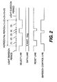
- FIG. 2 A control method for compensating Vth and mobility of the driving transistor 2 using the pixel 14 of FIG. 1 is shown in FIG. 2 .
- one horizontal period is divided into a reset period (1), a first data write period (2), a current supply period (3), a mobility compensation period (4), and a second data write period (5).
- the selection line 10 is made Low to select the line of pixels.
- the reset line 11 is made Low, the selection transistor 3 and the reset transistor 4 are turned on, and the drive transistor 2 is diode connected to enable current to temporarily flow in the organic EL element 1.
- the light emission control line 12 is made High and the light emission control transistor 5 is turned off, the current that was flowing in the organic EL element 1 is made to flow via the reset transistor 4 to the coupling capacitor 6 and storage capacitor 7.
- the selection line 10 High that potential is written to the storage capacitor 7 (above described Vgs is retained), and the first data write period (2) is completed.
- the previously described reset period does not have to continue until there is substantially no current flow in the driving transistor 2, and can be a length of time such as a few ⁇ s to a few tens of ⁇ s.
- the capacitance Cc of the coupling capacitor 6 is sufficiently larger than the capacitance Cs of the storage capacitor 7, which shows that Cc/(Cc+Cs) is substantially equal to 1, and the dynamic range of the gradation signal potential Vsig is maintained.
- mobility compensation current is large, that is, the drain potential of the driving transistor 2 is increased, which shows that a higher potential is written to the coupling transistor 6, while in the case of low mobility the mobility compensation current is small and the drain potential of the driving transistor 2 is lowered, which shows that a lower potential is written.
- the correction signal potential written to the coupling capacitor 6 is reflected at the gate terminal of the driving transistor 2, and by making the selection line 10 High a mobility corrected potential is written to the storage capacitor 7.
- the selection line 10 is then made High and the light emission control line 12 made Low, to complete the second data write period (5).
- FIG. 3 shows I-V curves for a driving transistor a and a driving transistor b with Vth compensated. If mobility differs, a difference in the inclination of the I-V curve arises between the transistors, and current flowing in the organic EL element 1 is different even if the same signal potential Vsig is applied. For example, even if Vsig1 is written to a pixel after Vth compensation, the transistor a and the transistor b with different mobility output respectively different drive currents of Ia(Vsig1) and Ib(Vsig1) to the organic EL element 1.
- a mobility compensated potential Vu corresponding to drive current Ids is subtracted from a potential across a gate and source with Vth compensated, which indicates that it is possible to make the drive current uniform.
- Vsig1 is written after compensation of Vth, with the transistor a current Ia(Vsig1) flows in the mobility compensation period, and with the transistor b current Ib(Vsig1) flows in the mobility compensation period, and these currents flow into the respective coupling capacitors 6 via the reset transistor 4.
- driving transistor b with a more upright I-V curve has greater current mobility compensation current than transistor a, and mobility compensation potential Vu is larger.
- driving transistor b since Vu(Ib(Vsig1)) > Vu(Ia(Vsig1)), driving transistor b has a smaller gate source potential, and output current is constrained. As a result, after completion of mobility compensation, if a signal is again written to the storage capacitor 7 in the second write period the drive current output to the organic EL elements is substantially I(Vsig1), and differences in output current due to mobility of the driving transistors a and b are made uniform.
- the mobility compensation of this embodiment it is possible to vary the mobility compensation period ⁇ t by either changing a pulse width input to the reset line 11 or inputting pulses a plurality of times etc., and it is possible to easily adjust the mobility compensation potential Vu.
- Vu mobility compensation potential
- by setting the mobility compensation period ⁇ t long in the case of a panel with large variation in mobility, and setting the mobility compensation period ⁇ t short with a panel having only slight variation in mobility it is possible to avoid the drawbacks of insufficient or excessive compensation.
- a register for setting ⁇ t in a data driver and select driver that will be described later, to write an externally supplied setting value for ⁇ t in this register, and to carry out control in accordance with a value for ⁇ t written to the register by the select driver at the time of mobility compensation.
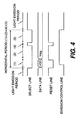
- FIG. 4 Another mobility compensation method using the pixels 14 of FIG. 1 is shown in FIG. 4 .
- the power supply period (3) is omitted from FIG. 4 .
- the mobility compensation current Ids is charged from the driving transistor 2 to the coupling capacitor 6.
- the current supply period (3) can be omitted in this way, control is simplified and it is possible to efficiently utilize the horizontal period. For example, the second write period can be sufficiently ensured, and the horizontal period can be shortened, and image signal writing can be simplified even if there are a lot of lines.
- Vth is compensated in the reset period, and after writing the gradation signal Vsig in the first write period mobility is compensated, and the description up to this point is the same as previously.
- the same gradation pixel is supplied to all pixels.
- the anode potential of the organic EL element 1 is written to one end of the coupling capacitor 6. While this is taking place, the other end of the coupling capacitor 6 is fixed at Vsig or another arbitrary potential. In this way, it is possible to read out an anode potential of the organic EL element at the time a fixed current flows, to the coupling capacitor 6.
- the drive potential rises with elapse of time if the flow of current continues in the organic EL element. Specifically, if the same current flows in a deteriorated organic EL element, the drive voltage increases.
- the potential read out to the coupling capacitor 6 in the drive voltage readout period reflects the extent of deterioration of the organic EL element, and a higher voltage is read out for organic EL elements that suffer greater deterioration.
- the selection line 10 is set low to commence the third write period (7), and the read out drive potential is reflected on the gate terminal of the drive transistor 2.
- Vtest is applied to the data line 8 in order to adjust the equalizing processing current, and an equalizing potential written to the storage capacitor 7 is adjusted using this adjustment potential Vtest to control current for the equalization processing.
- this equalization process is also possible for this equalization process to be carried out with a refresh rate of 60 Hz, the same as normal display, or to be carried out at a refresh rate that is different from that of normal display, such as a lower frequency of 30 Hz, for example. In this way a single horizontal period becomes longer, and it is made possible to sufficiently ensure the Vth compensation time and the deterioration potential readout time.
- the pixel 14 of this embodiment uses P-type transistors for all transistors, but it is also possible to use N-type transistors in some sections, or to use all N-type transistors.
- FIG 6 is one example of the pixel 14 constructed with N-type transistors, and is controlled on the basis of FIG. 2 and FIG 4 .
- an arbitrary potential for example, a cathode potential VSS
- VSS cathode potential
- the potential written to the coupling capacitor 6 and the storage capacitor 7 is not strictly speaking Vth of the driving transistor 2, but can be considered to reflect substantially Vth.
- the reset line 11 is set Low to turn the reset transistor 4 off and there is a transition to the first write period, a signal potential Vsig is supplied to the data line 8, and a signal potential Vsig with Vth compensated is written to the storage capacitor 7.
- the selection line 10 is set Low, and if the reset line 11 is set High and the reset transistor 4 is turned on in order to carry out mobility compensation a current corresponding to the gradation signal Vsig flows from the driving transistor 2 operated in the saturation region through the reset transistor 4 to discharge the coupling capacitor 6.
- the discharge amount is dependent on the mobility of the driving transistor 2, and so a potential having the mobility compensated is generated at the coupling capacitor. If the reset line 11 is set Low, the reset transistor turned off and the selection line 10 again set High, the select transistor 3 is turned on and the gradation potential with mobility compensated is written to the storage capacitor 7 and that potential is held by setting the select line to Low. Following that, by setting the light emission control line 5 High, a current with Vth and mobility compensated flows in the organic EL element 1, and the organic EL element emits light. That is, the mobility compensation of the present invention also acts efficiently if N-type transistors are used.
- FIG. 7 shows the pixel 14 with the anode of the organic EL element 1 made common. Therefore, VDD is supplied to the anode 13 while VSS is supplied to the power supply line 9. Control of the pixel 14 can use the same method as in FIG. 2 and FIG. 4 , but the polarities of pulses input to the selection line 10, reset line 11 and emission control line 12 are reversed. In the reset period, while VSS is being supplied to the data line 8, the selection line 10 and reset line 11 are made High, and the selection transistor 3 and the reset transistor 4 are turned on to diode connect the driving transistor 2.
- this compensation potential is held at the coupling capacitor 6, and in the second write period if the selection line 10 is again set High to turn the selection transistor 3 on then the compensation potential held at the coupling capacitor 6 is written to the storage capacitor 7. If the select transistor 3 is turned off and the light emission control transistor 5 is turned on, current flows in the organic EL element 1.
- equalization current can be adjusted using Vtest supplied to the data line 8.
- Vtest supplied to the data line 8.
- control is carried out so as to write a difference between Vsig and Vth to the coupling capacitor 6 in the reset period, and commence flow of current to the driving transistor 2 when the potential of the data line 8 becomes Vsig. Accordingly, if Vref is written in the first write period, a difference between Vref and Vsig is reflected at the gate of the driving transistor 2, and added to Vth, and so Vth is compensated.
- the selection transistor 3 and the light emission control transistor 5 are kept off, and the reset transistor 4 is turned on, to write a difference in mobility to the coupling capacitor 6 as a potential difference.
- this potential is written to the storage capacitor 7 to carry out mobility compensation. In this way, mobility compensation of this embodiment is utilized efficiently, even if the Vth compensation method is different.
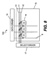
- FIG. 8 shows the overall structure of an organic EL display 100 formed from an array of the pixels 14 of the present invention.
- the organic EL display 100 includes a pixel array 15 having pixels 14 arranged in an array on a glass substrate or plastic substrate etc., a data driver 16 for driving data lines 8, and a selection driver 17 for driving select lines 10, reset line 11, and emission control lines 12.
- power supply lines 8 and cathode electrodes 13 that are common to all pixels are omitted from the drawing.
- a pixel array 15 an example of full-color pixels is shown formed from R (red) G (green) and B (blue) sub-pixels, but it is also possible to have a structure where W (white) is added to give full-color pixels of RGBW.
- the data driver 16 converts image data that has been transferred in dot units from an external section to line unit data using a shift register or the like, and outputs an analog signal potential in line units to the data line 8 by way of digital to analog conversion.
- Vth in order to write Vth, VDD and VSS signal potentials are output, but in the write period a gradation signal potential Vsig is supplied.
- Vsig gradation signal potential
- the selection driver 17 has three outputs per one line, specifically output to drive the select lines 10, output to drive the reset lines 11, and output to drive the light emission control lines 12, but the respective lines are selectively driven to be made High or Low at the timing of FIG 4 and FIG. 5 .
- the data driver 16 and the selection driver 17 can be formed from elements such as low temperature polysilicon on the same substrate as the pixels 14, or can be provided as driver ICs with the outputs of these ICs connected to each of the lines. From the structure of FIG 8 , Vth compensation and mobility compensation, and also equalization of deterioration of the organic EL elements, is carried out efficiently in the pixels 14.
- the structure of this embodiment can be used not only with organic EL elements, but with any other display device that uses current driven type light emitting elements.
Landscapes
- Engineering & Computer Science (AREA)
- Physics & Mathematics (AREA)
- Computer Hardware Design (AREA)
- General Physics & Mathematics (AREA)
- Theoretical Computer Science (AREA)
- Control Of El Displays (AREA)
- Electroluminescent Light Sources (AREA)
- Control Of Indicators Other Than Cathode Ray Tubes (AREA)
Claims (5)
- Anzeigevorrichtung mit einer Stromversorgung, die in einer Matrixform angeordnete Pixel aufweist, wobei jedes Pixel aufweist:einen Koppelkondensator (6), wobei ein Ende mit einer Datenleitung (8) verbunden ist;einen Auswahltransistor (3) mit zwei Enden und einem Steueranschluss, wobei ein Ende mit dem anderen Ende des Koppelkondensators (6) verbunden ist, und der dazu ausgebildet ist, durch eine mit dem Steueranschluss davon verbundene Auswahlleitung zwischen den Zuständen AN (ON) und AUS (OFF) schaltbar zu sein;einen Treibertransistor (2) mit zwei Enden und einem Steueranschluss, wobei der Steueranschluss davon mit dem anderen Ende des Auswahltransistors (3) verbunden ist, und ein Ende mit der Stromversorgung verbunden ist;einen Steuertransistor (5) der Lichtausstrahlung mit zwei Enden und einem Steueranschluss, wobei ein Ende mit dem anderen Ende des Treibertransistors (2) verbunden ist, und der dazu ausgebildet ist, über eine Steuerleitung der Lichtausstrahlung an- und ausgeschaltet zu werden;ein Lichtausstrahlungselement (1) eines strombetriebenen Typs, das mit dem anderen Ende des Steuertransistors (5) der Lichtausstrahlung verbunden ist;einen Speicherkondensator (7), der den Steueranschluss des Treibertransistors (2) und das eine Ende des Treibertransistors (2) verbindet, das mit der Stromversorgungsseite verbunden ist;einen Reset-Transistor (4) mit zwei Enden und einem Steueranschluss, wobei die beiden Enden des Reset-Transistors jeweils mit dem anderen Ende des Treibertransistors (2), an der Seite des Steuertransistors der Lichtausstrahlung, und mit dem anderen Ende des Koppelkondensators (6), auf der Seite des Auswahltransistors, verbunden sind, wobei der Reset-Transistor dazu ausgebildet ist, durch eine Reset-Leitung (11) an- und ausgeschaltet zu werden; undeinen Treiber, der dazu ausgebildet ist, die Spannung einer jeden der Leitungen zu steuern, indem eine Datenspannung, die einem der Datenleitung (8) zugeführten Gradationssignal entspricht, in den Speicherkondensator (7) über den Koppelkondensator (6) geschrieben wird, und eine Kompensationsspannung gemäß der Mobilität des Treibertransistors (2) in den Koppelkondensator (6) zu schreiben, wobei das Schreiben der Kompensationsspannung stattfindet, während der Auswahltransistor (3) und der Steuertransistor (5) der Lichtabstrahlung sich in einem ausgeschalteten Zustand befinden und der Reset-Transistor (4) eingeschaltet ist.
- Anzeigevorrichtung nach Anspruch 1, wobei die Lichtausstrahlungselemente (1) des stromgesteuerten Typs organische EL-Bauteile sind.
- Anzeigevorrichtung nach Anspruch 1, wobei der Treiber in der Lage ist, die Zeit zu variieren, die der Reset-Transistor (4) angeschaltet ist, während der Auswahltransistor (3) und die Steuertransistoren (5) der Lichtausstrahlung sich in einem ausgeschalteten Zustand befinden.
- Anzeigevorrichtung nach Anspruch 1, wobei der Treiber dazu ausgebildet ist, den Steuertransistor (5) der Lichtausstrahlung in einem Zustand einzuschalten, in dem der Auswahltransistor (3) und der Reset-Transistor (4) ausgeschaltet sind, und danach den Reset-Transistor (4) anzuschalten, wobei der Auswahltransistor (3) und der Steuertransistor (5) der Lichtausstrahlung ausgeschaltet sind.
- Anzeigevorrichtung nach Anspruch 1, wobei der Treiber dazu ausgebildet ist, eine Korrekturspannung in den Koppelkondensator (6) in einem Zustand zu schreiben, in dem allen Pixeln das gleiche Gradationssignal bereitgestellt wird, dann den Auswahltransistor (3) auszuschalten, den Steuertransistor (5) der Lichtausstrahlung und den Reset-Transistor (4) einzuschalten, und eine Spannung, die einer Spannungssenkung des Treibertransistors (2) entspricht, in den Koppelkondensator (6) zu schreiben, und danach eine Abgleichsverarbeitung der Stromeigenschalten des Treibertransistors (2) durchzuführen, indem das Fließen eines Stroms im Treibertransistor (2) basierend auf einer Spannung am Koppelkondensators (6) veranlasst wird.
Applications Claiming Priority (2)
| Application Number | Priority Date | Filing Date | Title |
|---|---|---|---|
| JP2008267708A JP5260230B2 (ja) | 2008-10-16 | 2008-10-16 | 表示装置 |
| PCT/US2009/005466 WO2010044827A1 (en) | 2008-10-16 | 2009-10-05 | Display device with compensation for variations in pixel transistors mobility |
Publications (2)
| Publication Number | Publication Date |
|---|---|
| EP2345023A1 EP2345023A1 (de) | 2011-07-20 |
| EP2345023B1 true EP2345023B1 (de) | 2013-01-16 |
Family
ID=41429414
Family Applications (1)
| Application Number | Title | Priority Date | Filing Date |
|---|---|---|---|
| EP09789397A Active EP2345023B1 (de) | 2008-10-16 | 2009-10-05 | Anzeigeanordnung mit kompensation von schwankungen der pixeltransistormobilität |
Country Status (6)
| Country | Link |
|---|---|
| US (1) | US8816943B2 (de) |
| EP (1) | EP2345023B1 (de) |
| JP (1) | JP5260230B2 (de) |
| KR (1) | KR101578761B1 (de) |
| CN (1) | CN102246221B (de) |
| WO (1) | WO2010044827A1 (de) |
Families Citing this family (14)
| Publication number | Priority date | Publication date | Assignee | Title |
|---|---|---|---|---|
| JP2010249955A (ja) * | 2009-04-13 | 2010-11-04 | Global Oled Technology Llc | 表示装置 |
| CN102915700B (zh) * | 2011-08-04 | 2015-11-25 | 昆山维信诺显示技术有限公司 | 有源oled照明装置 |
| JP2013222011A (ja) * | 2012-04-16 | 2013-10-28 | Samsung R&D Institute Japan Co Ltd | 駆動回路、電気光学装置、電子機器、および駆動方法 |
| US9747834B2 (en) * | 2012-05-11 | 2017-08-29 | Ignis Innovation Inc. | Pixel circuits including feedback capacitors and reset capacitors, and display systems therefore |
| JP2015197477A (ja) * | 2014-03-31 | 2015-11-09 | ソニー株式会社 | 信号処理方法、表示装置、及び電子機器 |
| KR102206287B1 (ko) * | 2014-06-13 | 2021-01-25 | 삼성디스플레이 주식회사 | 표시 장치 및 표시 장치의 구동 방법 |
| JP2018019335A (ja) * | 2016-07-29 | 2018-02-01 | ソニー株式会社 | 撮像素子および撮像装置 |
| KR102522534B1 (ko) * | 2016-07-29 | 2023-04-18 | 엘지디스플레이 주식회사 | 유기발광 표시장치와 그 구동방법 |
| KR102621655B1 (ko) | 2017-01-09 | 2024-01-09 | 삼성디스플레이 주식회사 | 화소 및 이를 이용한 유기전계발광 표시장치 |
| CN208335702U (zh) * | 2018-05-14 | 2019-01-04 | 北京京东方技术开发有限公司 | 显示面板及显示装置 |
| CN110111722A (zh) * | 2019-06-11 | 2019-08-09 | 惠州市华星光电技术有限公司 | 一种像素阵列 |
| CN111028767B (zh) * | 2019-12-06 | 2021-03-16 | 深圳市华星光电半导体显示技术有限公司 | 像素电路及驱动方法 |
| KR102785584B1 (ko) | 2020-10-05 | 2025-03-26 | 삼성전자주식회사 | 디스플레이 장치 |
| JP2024093381A (ja) | 2022-12-27 | 2024-07-09 | セイコーエプソン株式会社 | 表示装置および電子機器 |
Family Cites Families (27)
| Publication number | Priority date | Publication date | Assignee | Title |
|---|---|---|---|---|
| US6229506B1 (en) | 1997-04-23 | 2001-05-08 | Sarnoff Corporation | Active matrix light emitting diode pixel structure and concomitant method |
| WO1998048403A1 (en) | 1997-04-23 | 1998-10-29 | Sarnoff Corporation | Active matrix light emitting diode pixel structure and method |
| JP3767877B2 (ja) * | 1997-09-29 | 2006-04-19 | 三菱化学株式会社 | アクティブマトリックス発光ダイオード画素構造およびその方法 |
| US6348906B1 (en) * | 1998-09-03 | 2002-02-19 | Sarnoff Corporation | Line scanning circuit for a dual-mode display |
| JP2000148086A (ja) * | 1998-11-09 | 2000-05-26 | Pioneer Electronic Corp | 発光ディスプレイ装置および駆動方法 |
| JP4982014B2 (ja) | 2001-06-21 | 2012-07-25 | 株式会社日立製作所 | 画像表示装置 |
| JP4230744B2 (ja) * | 2001-09-29 | 2009-02-25 | 東芝松下ディスプレイテクノロジー株式会社 | 表示装置 |
| JP4974471B2 (ja) * | 2004-04-12 | 2012-07-11 | 三洋電機株式会社 | 有機el画素回路およびその駆動方法 |
| KR100560449B1 (ko) * | 2004-04-29 | 2006-03-13 | 삼성에스디아이 주식회사 | 발광 표시 패널 및 발광 표시 장치 |
| JP2006106141A (ja) | 2004-09-30 | 2006-04-20 | Sanyo Electric Co Ltd | 有機el画素回路 |
| KR100604066B1 (ko) * | 2004-12-24 | 2006-07-24 | 삼성에스디아이 주식회사 | 화소 및 이를 이용한 발광 표시장치 |
| JP5081374B2 (ja) | 2005-01-17 | 2012-11-28 | 株式会社ジャパンディスプレイイースト | 画像表示装置 |
| CA2496642A1 (en) * | 2005-02-10 | 2006-08-10 | Ignis Innovation Inc. | Fast settling time driving method for organic light-emitting diode (oled) displays based on current programming |
| JP2006284916A (ja) * | 2005-03-31 | 2006-10-19 | Toshiba Matsushita Display Technology Co Ltd | 表示装置、アレイ基板、及び表示装置の駆動方法 |
| JP4752331B2 (ja) * | 2005-05-25 | 2011-08-17 | セイコーエプソン株式会社 | 発光装置、その駆動方法及び駆動回路、並びに電子機器 |
| KR100754131B1 (ko) * | 2005-08-01 | 2007-08-30 | 삼성에스디아이 주식회사 | 데이터 구동회로와 이를 이용한 유기 발광 표시장치 및그의 구동방법 |
| JP2007108381A (ja) * | 2005-10-13 | 2007-04-26 | Sony Corp | 表示装置および表示装置の駆動方法 |
| JP2007316454A (ja) | 2006-05-29 | 2007-12-06 | Sony Corp | 画像表示装置 |
| JP4211820B2 (ja) | 2006-08-15 | 2009-01-21 | ソニー株式会社 | 画素回路と画像表示装置及びその駆動方法 |
| JP5261900B2 (ja) | 2006-08-23 | 2013-08-14 | ソニー株式会社 | 画素回路 |
| KR100805597B1 (ko) * | 2006-08-30 | 2008-02-20 | 삼성에스디아이 주식회사 | 화소 및 이를 이용한 유기전계발광 표시장치 및 그의구동방법 |
| JP4256888B2 (ja) | 2006-10-13 | 2009-04-22 | 株式会社 日立ディスプレイズ | 表示装置 |
| JP4596176B2 (ja) * | 2006-11-06 | 2010-12-08 | 株式会社 日立ディスプレイズ | 画像表示装置 |
| JP4300490B2 (ja) | 2007-02-21 | 2009-07-22 | ソニー株式会社 | 表示装置及びその駆動方法と電子機器 |
| JP5342111B2 (ja) * | 2007-03-09 | 2013-11-13 | 株式会社ジャパンディスプレイ | 有機el表示装置 |
| JP5352101B2 (ja) * | 2008-03-19 | 2013-11-27 | グローバル・オーエルイーディー・テクノロジー・リミテッド・ライアビリティ・カンパニー | 表示パネル |
| US8405582B2 (en) | 2008-06-11 | 2013-03-26 | Samsung Display Co., Ltd. | Organic light emitting display and driving method thereof |
-
2008
- 2008-10-16 JP JP2008267708A patent/JP5260230B2/ja active Active
-
2009
- 2009-10-05 US US13/123,696 patent/US8816943B2/en active Active
- 2009-10-05 CN CN200980150416.9A patent/CN102246221B/zh active Active
- 2009-10-05 KR KR1020117010704A patent/KR101578761B1/ko active Active
- 2009-10-05 WO PCT/US2009/005466 patent/WO2010044827A1/en not_active Ceased
- 2009-10-05 EP EP09789397A patent/EP2345023B1/de active Active
Also Published As
| Publication number | Publication date |
|---|---|
| JP5260230B2 (ja) | 2013-08-14 |
| WO2010044827A1 (en) | 2010-04-22 |
| KR20110071114A (ko) | 2011-06-28 |
| US8816943B2 (en) | 2014-08-26 |
| CN102246221A (zh) | 2011-11-16 |
| EP2345023A1 (de) | 2011-07-20 |
| KR101578761B1 (ko) | 2015-12-18 |
| CN102246221B (zh) | 2013-11-06 |
| US20110279049A1 (en) | 2011-11-17 |
| JP2010096990A (ja) | 2010-04-30 |
Similar Documents
| Publication | Publication Date | Title |
|---|---|---|
| US8736525B2 (en) | Display device using capacitor coupled light emission control transistors for mobility correction | |
| EP2345023B1 (de) | Anzeigeanordnung mit kompensation von schwankungen der pixeltransistormobilität | |
| JP5562327B2 (ja) | 表示装置及びその駆動方法 | |
| US8665186B2 (en) | Image display device and method of driving the same | |
| CN101884061B (zh) | 具有控制电路的led显示器 | |
| US9552760B2 (en) | Display panel | |
| JP2015025978A (ja) | 駆動回路、表示装置、及び駆動方法 | |
| US7944415B2 (en) | Organic light emitting diode display device and a driving method thereof | |
| US7586468B2 (en) | Display device using current driving pixels | |
| US7719497B2 (en) | Current feedback-type AMOLED where sense feedback is sent over the adjacent data line | |
| JP4838502B2 (ja) | 画像表示装置とその製造方法 | |
| KR102494924B1 (ko) | 유기발광 표시장치와 그 구동방법 | |
| JP5627311B2 (ja) | 表示装置およびその駆動方法 | |
| JP7469220B2 (ja) | 発光表示装置及び発光表示装置の駆動方法 | |
| CN102314831B (zh) | 显示设备及其显示驱动方法 | |
| JP4502602B2 (ja) | 表示装置 | |
| JP2008122498A (ja) | 表示パネルの駆動回路、表示装置および画素回路の駆動方法 |
Legal Events
| Date | Code | Title | Description |
|---|---|---|---|
| PUAI | Public reference made under article 153(3) epc to a published international application that has entered the european phase |
Free format text: ORIGINAL CODE: 0009012 |
|
| 17P | Request for examination filed |
Effective date: 20110420 |
|
| AK | Designated contracting states |
Kind code of ref document: A1 Designated state(s): AT BE BG CH CY CZ DE DK EE ES FI FR GB GR HR HU IE IS IT LI LT LU LV MC MK MT NL NO PL PT RO SE SI SK SM TR |
|
| AX | Request for extension of the european patent |
Extension state: AL BA RS |
|
| RIN1 | Information on inventor provided before grant (corrected) |
Inventor name: KAWABE, KAZUYOSHI |
|
| RAP1 | Party data changed (applicant data changed or rights of an application transferred) |
Owner name: GLOBAL OLED TECHNOLOGY LLC |
|
| DAX | Request for extension of the european patent (deleted) | ||
| GRAP | Despatch of communication of intention to grant a patent |
Free format text: ORIGINAL CODE: EPIDOSNIGR1 |
|
| GRAS | Grant fee paid |
Free format text: ORIGINAL CODE: EPIDOSNIGR3 |
|
| GRAA | (expected) grant |
Free format text: ORIGINAL CODE: 0009210 |
|
| AK | Designated contracting states |
Kind code of ref document: B1 Designated state(s): AT BE BG CH CY CZ DE DK EE ES FI FR GB GR HR HU IE IS IT LI LT LU LV MC MK MT NL NO PL PT RO SE SI SK SM TR |
|
| REG | Reference to a national code |
Ref country code: GB Ref legal event code: FG4D |
|
| REG | Reference to a national code |
Ref country code: CH Ref legal event code: EP |
|
| REG | Reference to a national code |
Ref country code: IE Ref legal event code: FG4D |
|
| REG | Reference to a national code |
Ref country code: AT Ref legal event code: REF Ref document number: 594254 Country of ref document: AT Kind code of ref document: T Effective date: 20130215 Ref country code: CH Ref legal event code: EP |
|
| REG | Reference to a national code |
Ref country code: DE Ref legal event code: R096 Ref document number: 602009012881 Country of ref document: DE Effective date: 20130314 |
|
| REG | Reference to a national code |
Ref country code: NL Ref legal event code: T3 |
|
| REG | Reference to a national code |
Ref country code: AT Ref legal event code: MK05 Ref document number: 594254 Country of ref document: AT Kind code of ref document: T Effective date: 20130116 |
|
| REG | Reference to a national code |
Ref country code: LT Ref legal event code: MG4D |
|
| PG25 | Lapsed in a contracting state [announced via postgrant information from national office to epo] |
Ref country code: AT Free format text: LAPSE BECAUSE OF FAILURE TO SUBMIT A TRANSLATION OF THE DESCRIPTION OR TO PAY THE FEE WITHIN THE PRESCRIBED TIME-LIMIT Effective date: 20130116 Ref country code: ES Free format text: LAPSE BECAUSE OF FAILURE TO SUBMIT A TRANSLATION OF THE DESCRIPTION OR TO PAY THE FEE WITHIN THE PRESCRIBED TIME-LIMIT Effective date: 20130427 Ref country code: SE Free format text: LAPSE BECAUSE OF FAILURE TO SUBMIT A TRANSLATION OF THE DESCRIPTION OR TO PAY THE FEE WITHIN THE PRESCRIBED TIME-LIMIT Effective date: 20130116 Ref country code: BE Free format text: LAPSE BECAUSE OF FAILURE TO SUBMIT A TRANSLATION OF THE DESCRIPTION OR TO PAY THE FEE WITHIN THE PRESCRIBED TIME-LIMIT Effective date: 20130116 Ref country code: BG Free format text: LAPSE BECAUSE OF FAILURE TO SUBMIT A TRANSLATION OF THE DESCRIPTION OR TO PAY THE FEE WITHIN THE PRESCRIBED TIME-LIMIT Effective date: 20130416 Ref country code: IS Free format text: LAPSE BECAUSE OF FAILURE TO SUBMIT A TRANSLATION OF THE DESCRIPTION OR TO PAY THE FEE WITHIN THE PRESCRIBED TIME-LIMIT Effective date: 20130516 Ref country code: NO Free format text: LAPSE BECAUSE OF FAILURE TO SUBMIT A TRANSLATION OF THE DESCRIPTION OR TO PAY THE FEE WITHIN THE PRESCRIBED TIME-LIMIT Effective date: 20130416 Ref country code: LT Free format text: LAPSE BECAUSE OF FAILURE TO SUBMIT A TRANSLATION OF THE DESCRIPTION OR TO PAY THE FEE WITHIN THE PRESCRIBED TIME-LIMIT Effective date: 20130116 |
|
| PG25 | Lapsed in a contracting state [announced via postgrant information from national office to epo] |
Ref country code: SI Free format text: LAPSE BECAUSE OF FAILURE TO SUBMIT A TRANSLATION OF THE DESCRIPTION OR TO PAY THE FEE WITHIN THE PRESCRIBED TIME-LIMIT Effective date: 20130116 Ref country code: FI Free format text: LAPSE BECAUSE OF FAILURE TO SUBMIT A TRANSLATION OF THE DESCRIPTION OR TO PAY THE FEE WITHIN THE PRESCRIBED TIME-LIMIT Effective date: 20130116 Ref country code: PT Free format text: LAPSE BECAUSE OF FAILURE TO SUBMIT A TRANSLATION OF THE DESCRIPTION OR TO PAY THE FEE WITHIN THE PRESCRIBED TIME-LIMIT Effective date: 20130516 Ref country code: PL Free format text: LAPSE BECAUSE OF FAILURE TO SUBMIT A TRANSLATION OF THE DESCRIPTION OR TO PAY THE FEE WITHIN THE PRESCRIBED TIME-LIMIT Effective date: 20130116 Ref country code: GR Free format text: LAPSE BECAUSE OF FAILURE TO SUBMIT A TRANSLATION OF THE DESCRIPTION OR TO PAY THE FEE WITHIN THE PRESCRIBED TIME-LIMIT Effective date: 20130417 Ref country code: LV Free format text: LAPSE BECAUSE OF FAILURE TO SUBMIT A TRANSLATION OF THE DESCRIPTION OR TO PAY THE FEE WITHIN THE PRESCRIBED TIME-LIMIT Effective date: 20130116 |
|
| PG25 | Lapsed in a contracting state [announced via postgrant information from national office to epo] |
Ref country code: HR Free format text: LAPSE BECAUSE OF FAILURE TO SUBMIT A TRANSLATION OF THE DESCRIPTION OR TO PAY THE FEE WITHIN THE PRESCRIBED TIME-LIMIT Effective date: 20130116 |
|
| PG25 | Lapsed in a contracting state [announced via postgrant information from national office to epo] |
Ref country code: EE Free format text: LAPSE BECAUSE OF FAILURE TO SUBMIT A TRANSLATION OF THE DESCRIPTION OR TO PAY THE FEE WITHIN THE PRESCRIBED TIME-LIMIT Effective date: 20130116 Ref country code: DK Free format text: LAPSE BECAUSE OF FAILURE TO SUBMIT A TRANSLATION OF THE DESCRIPTION OR TO PAY THE FEE WITHIN THE PRESCRIBED TIME-LIMIT Effective date: 20130116 Ref country code: CZ Free format text: LAPSE BECAUSE OF FAILURE TO SUBMIT A TRANSLATION OF THE DESCRIPTION OR TO PAY THE FEE WITHIN THE PRESCRIBED TIME-LIMIT Effective date: 20130116 Ref country code: RO Free format text: LAPSE BECAUSE OF FAILURE TO SUBMIT A TRANSLATION OF THE DESCRIPTION OR TO PAY THE FEE WITHIN THE PRESCRIBED TIME-LIMIT Effective date: 20130116 Ref country code: SK Free format text: LAPSE BECAUSE OF FAILURE TO SUBMIT A TRANSLATION OF THE DESCRIPTION OR TO PAY THE FEE WITHIN THE PRESCRIBED TIME-LIMIT Effective date: 20130116 |
|
| PLBE | No opposition filed within time limit |
Free format text: ORIGINAL CODE: 0009261 |
|
| STAA | Information on the status of an ep patent application or granted ep patent |
Free format text: STATUS: NO OPPOSITION FILED WITHIN TIME LIMIT |
|
| PG25 | Lapsed in a contracting state [announced via postgrant information from national office to epo] |
Ref country code: CY Free format text: LAPSE BECAUSE OF FAILURE TO SUBMIT A TRANSLATION OF THE DESCRIPTION OR TO PAY THE FEE WITHIN THE PRESCRIBED TIME-LIMIT Effective date: 20130116 |
|
| 26N | No opposition filed |
Effective date: 20131017 |
|
| PG25 | Lapsed in a contracting state [announced via postgrant information from national office to epo] |
Ref country code: IT Free format text: LAPSE BECAUSE OF FAILURE TO SUBMIT A TRANSLATION OF THE DESCRIPTION OR TO PAY THE FEE WITHIN THE PRESCRIBED TIME-LIMIT Effective date: 20130116 |
|
| REG | Reference to a national code |
Ref country code: DE Ref legal event code: R097 Ref document number: 602009012881 Country of ref document: DE Effective date: 20131017 |
|
| PG25 | Lapsed in a contracting state [announced via postgrant information from national office to epo] |
Ref country code: MC Free format text: LAPSE BECAUSE OF FAILURE TO SUBMIT A TRANSLATION OF THE DESCRIPTION OR TO PAY THE FEE WITHIN THE PRESCRIBED TIME-LIMIT Effective date: 20130116 |
|
| REG | Reference to a national code |
Ref country code: CH Ref legal event code: PL |
|
| REG | Reference to a national code |
Ref country code: IE Ref legal event code: MM4A |
|
| PG25 | Lapsed in a contracting state [announced via postgrant information from national office to epo] |
Ref country code: LI Free format text: LAPSE BECAUSE OF NON-PAYMENT OF DUE FEES Effective date: 20131031 Ref country code: CH Free format text: LAPSE BECAUSE OF NON-PAYMENT OF DUE FEES Effective date: 20131031 |
|
| PG25 | Lapsed in a contracting state [announced via postgrant information from national office to epo] |
Ref country code: IE Free format text: LAPSE BECAUSE OF NON-PAYMENT OF DUE FEES Effective date: 20131005 |
|
| PG25 | Lapsed in a contracting state [announced via postgrant information from national office to epo] |
Ref country code: SM Free format text: LAPSE BECAUSE OF FAILURE TO SUBMIT A TRANSLATION OF THE DESCRIPTION OR TO PAY THE FEE WITHIN THE PRESCRIBED TIME-LIMIT Effective date: 20130116 |
|
| PG25 | Lapsed in a contracting state [announced via postgrant information from national office to epo] |
Ref country code: TR Free format text: LAPSE BECAUSE OF FAILURE TO SUBMIT A TRANSLATION OF THE DESCRIPTION OR TO PAY THE FEE WITHIN THE PRESCRIBED TIME-LIMIT Effective date: 20130116 |
|
| PG25 | Lapsed in a contracting state [announced via postgrant information from national office to epo] |
Ref country code: LU Free format text: LAPSE BECAUSE OF NON-PAYMENT OF DUE FEES Effective date: 20131005 Ref country code: MK Free format text: LAPSE BECAUSE OF FAILURE TO SUBMIT A TRANSLATION OF THE DESCRIPTION OR TO PAY THE FEE WITHIN THE PRESCRIBED TIME-LIMIT Effective date: 20130116 Ref country code: HU Free format text: LAPSE BECAUSE OF FAILURE TO SUBMIT A TRANSLATION OF THE DESCRIPTION OR TO PAY THE FEE WITHIN THE PRESCRIBED TIME-LIMIT; INVALID AB INITIO Effective date: 20091005 |
|
| PG25 | Lapsed in a contracting state [announced via postgrant information from national office to epo] |
Ref country code: MT Free format text: LAPSE BECAUSE OF FAILURE TO SUBMIT A TRANSLATION OF THE DESCRIPTION OR TO PAY THE FEE WITHIN THE PRESCRIBED TIME-LIMIT Effective date: 20130116 |
|
| REG | Reference to a national code |
Ref country code: FR Ref legal event code: PLFP Year of fee payment: 8 |
|
| REG | Reference to a national code |
Ref country code: FR Ref legal event code: PLFP Year of fee payment: 9 |
|
| REG | Reference to a national code |
Ref country code: FR Ref legal event code: PLFP Year of fee payment: 10 |
|
| PGFP | Annual fee paid to national office [announced via postgrant information from national office to epo] |
Ref country code: NL Payment date: 20251021 Year of fee payment: 17 |
|
| PGFP | Annual fee paid to national office [announced via postgrant information from national office to epo] |
Ref country code: DE Payment date: 20251021 Year of fee payment: 17 |
|
| PGFP | Annual fee paid to national office [announced via postgrant information from national office to epo] |
Ref country code: GB Payment date: 20251022 Year of fee payment: 17 |
|
| PGFP | Annual fee paid to national office [announced via postgrant information from national office to epo] |
Ref country code: FR Payment date: 20251029 Year of fee payment: 17 |