EP2345079B1 - Capteurs d'image cmos rétroéclairés - Google Patents
Capteurs d'image cmos rétroéclairés Download PDFInfo
- Publication number
- EP2345079B1 EP2345079B1 EP09752521.6A EP09752521A EP2345079B1 EP 2345079 B1 EP2345079 B1 EP 2345079B1 EP 09752521 A EP09752521 A EP 09752521A EP 2345079 B1 EP2345079 B1 EP 2345079B1
- Authority
- EP
- European Patent Office
- Prior art keywords
- layer
- sensor layer
- well
- sensor
- type dopant
- Prior art date
- Legal status (The legal status is an assumption and is not a legal conclusion. Google has not performed a legal analysis and makes no representation as to the accuracy of the status listed.)
- Active
Links
Images





Classifications
-
- H—ELECTRICITY
- H10—SEMICONDUCTOR DEVICES; ELECTRIC SOLID-STATE DEVICES NOT OTHERWISE PROVIDED FOR
- H10F—INORGANIC SEMICONDUCTOR DEVICES SENSITIVE TO INFRARED RADIATION, LIGHT, ELECTROMAGNETIC RADIATION OF SHORTER WAVELENGTH OR CORPUSCULAR RADIATION
- H10F39/00—Integrated devices, or assemblies of multiple devices, comprising at least one element covered by group H10F30/00, e.g. radiation detectors comprising photodiode arrays
- H10F39/10—Integrated devices
- H10F39/12—Image sensors
-
- H—ELECTRICITY
- H10—SEMICONDUCTOR DEVICES; ELECTRIC SOLID-STATE DEVICES NOT OTHERWISE PROVIDED FOR
- H10F—INORGANIC SEMICONDUCTOR DEVICES SENSITIVE TO INFRARED RADIATION, LIGHT, ELECTROMAGNETIC RADIATION OF SHORTER WAVELENGTH OR CORPUSCULAR RADIATION
- H10F39/00—Integrated devices, or assemblies of multiple devices, comprising at least one element covered by group H10F30/00, e.g. radiation detectors comprising photodiode arrays
- H10F39/10—Integrated devices
- H10F39/12—Image sensors
- H10F39/18—Complementary metal-oxide-semiconductor [CMOS] image sensors; Photodiode array image sensors
-
- H—ELECTRICITY
- H10—SEMICONDUCTOR DEVICES; ELECTRIC SOLID-STATE DEVICES NOT OTHERWISE PROVIDED FOR
- H10F—INORGANIC SEMICONDUCTOR DEVICES SENSITIVE TO INFRARED RADIATION, LIGHT, ELECTROMAGNETIC RADIATION OF SHORTER WAVELENGTH OR CORPUSCULAR RADIATION
- H10F39/00—Integrated devices, or assemblies of multiple devices, comprising at least one element covered by group H10F30/00, e.g. radiation detectors comprising photodiode arrays
- H10F39/011—Manufacture or treatment of image sensors covered by group H10F39/12
- H10F39/014—Manufacture or treatment of image sensors covered by group H10F39/12 of CMOS image sensors
-
- H—ELECTRICITY
- H10—SEMICONDUCTOR DEVICES; ELECTRIC SOLID-STATE DEVICES NOT OTHERWISE PROVIDED FOR
- H10F—INORGANIC SEMICONDUCTOR DEVICES SENSITIVE TO INFRARED RADIATION, LIGHT, ELECTROMAGNETIC RADIATION OF SHORTER WAVELENGTH OR CORPUSCULAR RADIATION
- H10F39/00—Integrated devices, or assemblies of multiple devices, comprising at least one element covered by group H10F30/00, e.g. radiation detectors comprising photodiode arrays
- H10F39/10—Integrated devices
- H10F39/12—Image sensors
- H10F39/199—Back-illuminated image sensors
-
- H—ELECTRICITY
- H10—SEMICONDUCTOR DEVICES; ELECTRIC SOLID-STATE DEVICES NOT OTHERWISE PROVIDED FOR
- H10F—INORGANIC SEMICONDUCTOR DEVICES SENSITIVE TO INFRARED RADIATION, LIGHT, ELECTROMAGNETIC RADIATION OF SHORTER WAVELENGTH OR CORPUSCULAR RADIATION
- H10F39/00—Integrated devices, or assemblies of multiple devices, comprising at least one element covered by group H10F30/00, e.g. radiation detectors comprising photodiode arrays
- H10F39/80—Constructional details of image sensors
- H10F39/807—Pixel isolation structures
-
- H—ELECTRICITY
- H10—SEMICONDUCTOR DEVICES; ELECTRIC SOLID-STATE DEVICES NOT OTHERWISE PROVIDED FOR
- H10F—INORGANIC SEMICONDUCTOR DEVICES SENSITIVE TO INFRARED RADIATION, LIGHT, ELECTROMAGNETIC RADIATION OF SHORTER WAVELENGTH OR CORPUSCULAR RADIATION
- H10F39/00—Integrated devices, or assemblies of multiple devices, comprising at least one element covered by group H10F30/00, e.g. radiation detectors comprising photodiode arrays
- H10F39/80—Constructional details of image sensors
- H10F39/806—Optical elements or arrangements associated with the image sensors
- H10F39/8063—Microlenses
Definitions
- the present invention relates to a method for fabricating a back-illuminated image sensors.
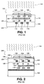
- FIG. 1 is a simplified illustration of a front-illuminated image sensor in accordance with the prior art.
- Image sensor 100 includes pixels 102, 104, 106 formed within a sensor layer 108 and a circuit layer 110.
- Photodetectors 112, 114, 116 are formed in sensor layer 108.
- Conductive interconnects 118, 120, 122, such as gates and connectors, are formed in circuit layer 110.
- a back-illuminated image sensor addresses the fill factor and quantum efficiency issues by constructing the image sensor such that the light from a subject scene is incident on a backside of a sensor layer.
- the "frontside" 126 of sensor layer 108 is conventionally known as the side of sensor layer 108 that abuts circuit layer 110, while the "backside” 128 is the side of sensor layer 108 that opposes frontside 126.
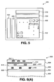
- FIG. 2 is a simplified illustration of a back-illuminated image sensor in accordance with the prior art.
- Circuit layer 110 is positioned between support substrate 202 and sensor layer 108. This allows light 124 to strike the backside 128 of sensor layer 108, where it is detected by photodetectors 112, 114, 116. The detection of light 124 by photodetectors 112, 114, 116 is no longer impacted by the metallization level interconnects and other features of circuit layer 110.
- Interface 204 between sensor layer 108 and insulating layer 206 can produce high levels of dark current and a loss of quantum efficiency, especially in the blue light spectrum. This is due to the presence of dangling bonds at the etched silicon surface of backside 128. Moreover, conventional passivation techniques for passivating interface 204 can be adversely impacted by subsequent processing steps during fabrication of image sensor 200.
- FIG. 3 depicts an exemplary doping profile of interface 204 along line A-A' in FIG. 2 .
- Conventional back-illuminated image sensors are constructed as n-type metal-oxide-semiconductor (NMOS) image sensor.
- NMOS metal-oxide-semiconductor
- the n-doped photodetectors are formed in a well or layer doped with one or more p-type dopants.
- Line 300 depicts a doping profile of boron dopants (p-type) at interface 204 prior to the performance of subsequent Complementary Metal Oxide Semiconductor (CMOS) fabrication steps on image sensor 200, while line 302 illustrates the doping profile of boron at interface 204 after the performance of the subsequent CMOS fabrication steps. As shown in FIG.
- CMOS Complementary Metal Oxide Semiconductor
- the boron dopants diffuse out of sensor layer 108 and into insulating layer 206 during the subsequent CMOS fabrication steps. This diffusion creates a drop in doping profile 304 on the sensor layer side of interface 204. The drop in the doping profile produces an unwanted electrostatic potential well that traps photo-induced charge carriers at interface 204. Substituting slower diffusing p-type dopants, such as indium, for boron can reduce the thermal diffusion during processing, but indium increases the number of dark field bright point defects in the image sensor.
- US 2006/186560 A1 describes a method for fabricating a back-illuminated semiconductor imaging device on a thin semiconductor-on-insulator substrate and the resulting imaging device.
- the resulting device is described as having a monotonically varying doping profile which provides a desired electric field and eliminates a dead band proximate to the backside surface.
- EP 1612863 A2 describes a back-illuminated solid-state imaging device that is described as being able to suppress a crystal defect caused by a metal contamination in a process and to suppress a dark current to improve quantum efficiency. Also described is a method of producing such a device. The method has the steps of forming a structure including a substrate, a first conductive type epitaxial layer and a first conductive type impurity layer. The first conductive type epitaxial layer is formed on the substrate to have a first impurity concentration, and the first conductive type impurity layer is formed in a boundary region to have a second impurity concentration higher than the first impurity concentration of the epitaxial layer. The method also includes forming a second conductive type region storing a charge generated by a photoelectric conversion in the epitaxial layer, forming an interconnection layer on the epitaxial layer and removing the substrate.
- WO 2005/046207 A2 describes an imager, an image sensor included in the imager and a method of fabricating the image sensor.
- the image sensor has a substrate with front and back sides to produce image data. It includes a transparent conductive coating arranged on the back side of the substrate, a first well region of a first conductive type having first and second opposite sides, the first side being arranged adjacent with the front side of the image sensor; and a second well region of a second conductive type, different from the first conductive type and having a deep well region provided adjacent with the second side of the first well region.
- the transparent conductive coating is configured to develop or to receive a first potential and the first well region is configured to receive a second potential to substantially deplete a region between the transparent conductive coating and the first well region.
- US 2007/235829 A1 describes a method for fabricating a back-illuminated semiconductor imaging device on a semiconductor-on-insulator substrate, and a resulting imaging device.
- the device includes an insulator layer; a semiconductor substrate having an interface with the insulator layer; an epitaxial layer grown on the semiconductor substrate by epitaxial growth; and one or more imaging components in the epitaxial layer in proximity to a face of the epitaxial layer, the face being opposite the interface of the semiconductor substrate and the insulator layer.
- the imaging components comprise junctions within the epitaxial layer.
- the semiconductor substrate and the epitaxial layer exhibit a net doping concentration having a maximum value at a predetermined distance from the interface of the insulating layer and the semiconductor substrate and which decreases monotonically on both sides of the profile from the maximum value within a portion of the semiconductor substrate and the epitaxial layer.
- the doping profile between the interface with the insulation layer and the peak of the doping profile functions as a "dead band" to prevent dark current carriers from penetrating to the front side of the device.
- EP 1653521 A1 describes a back illuminated photodetector having a back illuminated photodiode that comprises an N-type semiconductor substrate, a P + - type impurity semiconductor region, a recessed portion, and a window plate.
- the P + -type impurity semiconductor region In the surface layer on the upper surface side of the N-type semiconductor substrate is formed the P + -type impurity semiconductor region.
- the recessed portion In the rear surface of the N-type semiconductor substrate and in an area opposite the P + -type impurity semiconductor region is formed the recessed portion that functions as an incident part for to-be-detected light.
- the window plate is bonded to the outer edge portion of the recessed portion. The window plate covers the recessed portion and seals the rear surface of the N-type semiconductor substrate.
- a method for making a solid-state imaging device that can form a first P-type well region deep in a substrate without being affected by the heat applied during an epitaxial growth process.
- the method includes a first step of preparing a substrate composite comprising an first substrate and a second substrate on the first substrate, a second step of implanting impurity ions from the surface of the second substrate at an energy exceeding 3 MeV so as to form a barrier layer, and a third step of forming a photosensor in the second substrate.
- JP 2008/0210580 discloses a back irradiation image sensor which performs imaging by irradiating the back side of a p-substrate with light and reading out charges generated in the p-substrate depending on the light from the surface side.
- the p-substrate comprises a plurality of n-layers for storing the charges formed on the same plane near the surface of the p-substrate in the p-substrate, a plurality of n+ layers formed between the plurality of n-layers and the surface of the p-substrate, respectively, and functioning as an overflow drain for discharging unnecessary charges stored in the plurality of n-layers, respectively, and a plurality of p+ layers formed between the plurality of n+ layers and the plurality of n-layers, respectively, and functioning as an overflow barrier for the overflow drain.
- the n+ layer is formed at a position overlapping the maximum potential point (center) of the n-layer on the plan view.
- the n-type dopant or dopants in the well or buried well have a segregation coefficient that causes the n-type dopant to accumulate in the sensor layer side of an interface between the backside of the sensor layer and the insulating layer. This accumulation of the n-type dopant or dopants passivates the interface between the sensor layer and the insulating layer and prevents the formation of an electrostatic potential well at the interface. Additionally, the well or buried well can be biased at a predetermined potential with respect to ground for driving the photo-generated charges into the nearest respective photodetector in the sensor layer. The well or buried well can also include a doping gradient that steers the photo-generated charges into the nearest respective photodetector in the sensor layer. And finally, one or more active electronic components can be disposed in the sensor layer within each pixel, and electronic circuitry that is electrically connected to the imaging area can be disposed outside of the imaging area.
- n-type dopants in the well or buried well accumulate in the sensor layer side of an interface between the backside of the sensor layer and the insulating layer while the p-type dopants diminish in the sensor layer side of the interface.
- the combination of the increased concentration of the n-type dopant and the decreased concentration of the p-type dopant at the interface prevents the formation of a potential well in the sensor layer side of the interface.
- Doping of the well or buried well can occur after thermal oxidation of the shallow trench isolation regions. This minimizes the thermal diffusion of the dopants in the well or buried well.
- any photo-generated charge that is trapped at the interface between the sensor layer and the insulating layer during the fabrication process is typically positive in a PMOS image sensor. Positive charge directs the photo-generated charges toward the photodetectors and favorably passivates the interface.
- the terms such as “on” or “over”, when used in conjunction with layers of an image sensor wafer or corresponding image sensor, are intended to be construed broadly, and therefore should not be interpreted to preclude the presence of one or more intervening layers or other intervening image sensor features or elements.
- a given layer that is described herein as being formed on or formed over another layer may be separated from the latter layer by one or more additional layers.
- Image capture device 400 is implemented as a digital camera in FIG. 4 .
- a digital camera is only one example of an image capture device that can utilize an image sensor incorporating the present invention.
- Other types of image capture devices such as, for example, cell phone cameras and digital video camcorders, can be used with the present invention.
- Imaging stage 404 can include conventional elements such as a lens, a neutral density filter, an iris and a shutter. Light 402 is focused by imaging stage 404 to form an image on image sensor 406. Image sensor 406 captures one or more images by converting the incident light into electrical signals. Digital camera 400 further includes processor 408, memory 410, display 412, and one or more additional input/output (I/O) elements 414. Although shown as separate elements in the embodiment of FIG. 4 , imaging stage 404 may be integrated with image sensor 406, and possibly one or more additional elements of digital camera 400, to form a compact camera module.
- I/O input/output
- Processor 408 may be implemented, for example, as a microprocessor, a central processing unit (CPU), an application-specific integrated circuit (ASIC), a digital signal processor (DSP), or other processing device, or combinations of multiple such devices.
- Various elements of imaging stage 404 and image sensor 406 may be controlled by timing signals or other signals supplied from processor 408.
- Memory 410 may be configured as any type of memory, such as, for example, random access memory (RAM), read-only memory (ROM), Flash memory, disk-based memory, removable memory, or other types of storage elements, in any combination.
- RAM random access memory
- ROM read-only memory
- Flash memory disk-based memory
- removable memory or other types of storage elements, in any combination.
- a given image captured by image sensor 406 may be stored by processor 408 in memory 410 and presented on display 412.
- Display 412 is typically an active matrix color liquid crystal display (LCD), although other types of displays may be used.
- the additional I/O elements 414 may include, for example, various on-screen controls, buttons or other user interfaces, network interfaces, or memory card interfaces.
- the digital camera shown in FIG. 4 may comprise additional or alternative elements of a type known to those skilled in the art. Elements not specifically shown or described herein may be selected from those known in the art. As noted previously, the present invention may be implemented in a wide variety of image capture devices. Also, as mentioned above, certain aspects of the embodiments described herein may be implemented at least in part in the form of software executed by one or more processing elements of an image capture device. Such software can be implemented in a straightforward manner given the teachings provided herein, as will be appreciated by those skilled in the art.
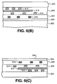
- FIG. 5 is a simplified block diagram of image sensor 406 shown in FIG. 4 in an embodiment in accordance with the invention.
- Image sensor 406 typically includes an array of pixels 500 that form an imaging area 502.
- Image sensor 406 further includes column decoder 504, row decoder 506, digital logic 508, and analog or digital output circuits 510.
- Image sensor 406 is implemented as a back-illuminated Complementary Metal Oxide Semiconductor (CMOS) image sensor in an embodiment in accordance with the invention.
- CMOS Complementary Metal Oxide Semiconductor
- column decoder 504, row decoder 506, digital logic 508, and analog or digital output circuits 510 are implemented as standard CMOS electronic circuits that are electrically connected to imaging area 502.
- Functionality associated with the sampling and readout of imaging area 502 and the processing of corresponding image data may be implemented at least in part in the form of software that is stored in memory 410 and executed by processor 408 (see FIG. 4 ). Portions of the sampling and readout circuitry may be arranged external to image sensor 406, or formed integrally with imaging area 502, for example, on a common integrated circuit with photodetectors and other elements of the imaging area. Those skilled in the art will recognize that other peripheral circuitry configurations or architectures can be implemented in other embodiments in accordance with the invention.
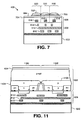
- FIGS. 6(A)-6(C) there are shown simplified cross-sectional views of a portion of an image sensor that are used to illustrate a method of fabricating a back-illuminated image sensor in an embodiment in accordance with the invention.
- FIG. 6 shows a portion of an image sensor wafer 600 at the completion of a number of initial steps of an exemplary CMOS fabrication process.
- Image sensor wafer 600 at this stage includes substrate 602, insulating layer 604 formed over substrate 602, sensor layer 606 formed over insulating layer 604, and circuit layer 608 formed over sensor layer 606.
- Various image sensor features, such as conductive interconnects 610, 612, gates 614, or other circuit elements can be formed within circuit layer 608 using conventional techniques.
- Sensor layer 606 is processed to form photodetectors 616 and other circuit elements within sensor layer 606.
- Sensor layer 606 has a frontside 618 and a backside 620.
- the "frontside” 618 of sensor layer 606 is conventionally known as the side of sensor layer 606 that is adjacent to circuit layer 608, while the "backside” 620 is the side of sensor layer 606 that opposes frontside 618.
- Substrate 602 and sensor layer 606 are typically formed with a silicon material, insulating layer 604 with a silicon dioxide material, and circuit layer 608 with a dielectric material in an embodiment in accordance with the invention.
- Interconnects 610, 612 and gates 614 in circuit layer 608 are associated with various metallization levels.
- Image sensor wafer 600 depicted in FIG. 6(A) is an example of a silicon-on-insulator (SOI) wafer.
- the thickness of the sensor layer 606 may be approximately 1 to 50 micrometers, and the thickness of insulating layer 604 may be approximately 0.1 to 3 micrometers, although other thicknesses may be used.
- Substrate 602 is typically substantially thicker than sensor layer 606 or insulating layer 604, and may be approximately 300 to 1000 micrometers in thickness.
- Other embodiments in accordance with the invention may use other types of wafers to form back-illuminated image sensors, such as, for example, epitaxial wafers or bulk semiconductor wafers that do not include an insulating layer 604.
- FIG. 6(B) illustrates image sensor wafer 600 after support wafer 622 is bonded to circuit layer 608.
- Support wafer 622 is typically bonded to circuit layer 608 with one or more adhesive layers (not shown), or bonded directly with the application of pressure or temperature.
- One example of a material that can be used for direct bonding is silicon dioxide.
- Substrate 602 is then removed, resulting in the image sensor wafer structure as shown in FIG. 6(C) .
- Substrate 602 may be removed using, for example, grinding, polishing or etching techniques, in any combination.
- Substrate 602 is removed in its entirety with insulating layer 604 acting as an etch stop in an embodiment in accordance with the invention.
- substrate 602 can be thinned rather than removed completely, and an insulating layer deposited onto the etched surface.
- processing steps may include the formation of a color filter array and associated microlenses on the backside 624 of insulating layer 604 (see FIG. 7 ).
- Image sensor 406 includes pixels 500 formed within a sensor layer 606 and a circuit layer 608.
- Photodetectors 616 are formed in sensor layer 606.
- Conductive interconnects 610, 612, 614, such as gates and connectors, are formed in circuit layer 608.
- Color filter elements 700 are shown formed on insulating layer 604. Also associated with each color filter element 700 is a corresponding microlens 702. Color filter elements 700 are arranged over respective photodetectors 616 and typically act as bandpass filters that allow each photodetector 616 to detect light propagating at particular wavelength ranges. For example, one color filter element permits light propagating in the wavelength range corresponding to red light to be detected by a photodetector while an adjacent color filter element allows light propagating in the wavelength range corresponding to green light to be detected by a photodetector.
- sensor layer 606 is formed in a manner that passivates interface 704 between sensor layer 606 and insulating layer 604 to reduce dark current and improve quantum efficiency. Moreover, sensor layer 606 is biased to a known potential with respect to ground to steer photo-generated charges, especially those charges generated near the back side surface of the back-illuminated image sensor, into the nearest photodetector. And finally, sensor layer 606 can include a dopant gradient that steers the photo-generated charges into the nearest photodetector. Steering the photo-generated charges into the nearest photodetector minimizes crosstalk and lag within the image sensor.
- FIG. 8 is a cross-sectional view of a first pixel structure in an embodiment in accordance with the invention.
- Pixel 500 includes photodetector 616 formed within well 800.
- Photodetector 616 is implemented as a photodiode in the embodiment of FIG. 8 .
- Pinning layer 802 is formed over photodetector 616.
- One or more shallow trench isolation (STI) regions 803 are formed within pixel 500.
- STI shallow trench isolation
- Transfer gate 804 is used to transfer the photo-generated charges from photodetector 616 to charge-to-voltage converter 806.
- Charge-to-voltage converter 806 is configured as a floating diffusion in an embodiment in accordance with the invention. Converter 806 converts the charge into a voltage signal.
- Source-follower transistor 808 buffers the voltage signal stored in charge-to-voltage converter 806.
- Reset transistor 806, 810, 812 is used to reset converter 806 to a known potential prior to pixel readout.
- Well 800 is biased to a known voltage level VDD through well contact 814. Biasing well 800 to a known potential with respect to ground steers the photo-generated charges into photodetector 616.
- Well contact 814 is positioned outside of imaging area 502 ( FIG. 5 ) at the periphery of image sensor 406 in an embodiment in accordance with the invention.
- Other well contacts 816 are periodically spaced throughout imaging area 502 ( FIG. 5 ) to reduce the effective resistance of well 800 and reduce or eliminate well bounce in the embodiment shown in FIG. 8 .
- Pixel 500 is based on p-type metal-oxide-semiconductor (PMOS) circuitry in an embodiment in accordance with the invention.
- photodetector 616 is doped with one or more p-type dopants and well 800 and pinning layer 802 are doped with one or more n-type dopants.
- n-type dopants include, but are not limited to, phosphorus, antimony, and arsenic. Boron and gallium are examples of p-type dopants.
- FIG. 9 depicts an exemplary doping profile of interface 704 along line C-C' in FIG. 8 in an embodiment in accordance with the invention.
- Line 900 illustrates the doping profile of a boron doped SOI wafer after oxidation of STI regions 803, while line 902 depicts the doping profile of implanted phosphorous dopants in well 800 after oxidation of the STI regions.
- both the boron and the phosphorous dopants diffuse during oxidation of the STI regions. Due to segregation, the phosphorus dopants accumulate on the silicon side of interface 704 (see point 904) while the boron dopants diminish on the silicon side of interface 704 (see point 906).
- the combination of the increased concentration of the n-type phosphorus dopants and the decreased concentration of the p-type boron dopants at interface 704 reduces or prevents the formation of a potential well on the sensor layer side of interface.
- the phosphorous segregation at interface 704 further improves the performance of an image sensor because the segregation coefficients between silicon and silicon dioxide for phosphorous and boron provide for an effective build-up of net n-type dopants on the silicon side of interface 704.
- This enhanced net n-type doping concentration in the silicon at interface 704 creates a potential gradient that directs photo-generated charges (i.e., holes) into the photodetector.
- the electric field gradient may be small, an electrostatic potential well like prior art well 304 (see FIG. 3 ) is not created at the surface.
- positive charge can be trapped at interface 704, which further directs the photo-generated charge towards the photodetector.
- n i is 1.6E10 cm-3. Therefore an electron concentration of 2E16 cm-3 at interface 704 will suppress the dark current generation from dangling silicon bonds by almost six orders of magnitude, effectively passivating interface 704. This is unlike the NMOS image sensor shown in FIG. 2 , where the effective n-dopant build-up on the silicon side of interface 204 produces a well in the boron concentration (see point 304 in FIG. 3 ).
- the dopants in well 800 can be doped such that an enhanced dopant gradient is formed in well 800.
- the dopant gradient is formed, for example, by performing a chain of implants that result in a greater number of n-type dopants at interface 704. This dopant gradient provides a more uniform electric field in well 800 so that photo-generated charges are driven more effectively into photodetector 616.
- FIG. 10 depicts an alternate exemplary doping profile of interface 704 along line C-C' in FIG. 8 when a chain of three phosphorous implants are implanted into well 800.
- Line 1000 depicts the phosphorous dopants after a deep well implant and before thermal oxidation of STI regions 803 ( FIG. 8 ).
- Line 1002 illustrates the phosphorous dopants after thermal oxidation of the STI regions.
- the STI oxidation thermally diffuses the n-type dopants in well 800 and removes the peaks and valleys in doping profile 1000. Removing the peaks and valleys reduces potential wells in the electrostatic profile between interface 704 and photodetector 616.
- n-type dopant in well 800 is phosphorous
- the phosphorous segregation at interface 704 improves lag and dark current performance as described earlier. It is worth noting again that the high energy implant doses required to define an n-type well 800 are much lower than the doses required to define a p-type well for a corresponding NMOS pixel with comparable lag and dark current performance.
- FIG. 11 there is shown a cross-sectional view of a portion of the standard CMOS circuitry in an example being useful to understand the present invention.
- the standard PMOS 1100 and NMOS 1102 transistors, and their associated shallow n-well 1104 and p-well 1106 implants are unaffected by the deep well implant 800 ( FIG. 8 ) in the imaging area 502 ( FIG. 5 ).
- the p-type 1100 and n-type 1102 transistors in the CMOS circuitry outside of imaging area 502 are fabricated using the standard CMOS process flow.
- the CMOS circuitry is protected from back illumination by an opaque lightshield (not shown) in an example being useful to understand the present invention.
- the lightshield can be metal, a stacked layer of red, green, and blue color filter array material, or a unique light absorbing material.
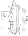
- FIG. 12 is a cross-sectional view of an alternate pixel structure in an embodiment in accordance with the invention.
- Pixel 500 includes a number of the same elements shown in FIG. 8 , and like reference numerals have been used to indicate such elements.
- Pixel 500 increases a depletion depth of photodetector 616 with region 1200 by effectively producing an "extension" of photodetector 616.
- Region 1200 is lightly doped with one or more p-type dopants in an embodiment in accordance with the invention.
- Buried well 1202 and side wells 1204, 1206 are doped with an n-type dopant and are formed such that p-region 1200 is created between photodetector 616, buried well 1202, and side wells 1204, 1206.
- Side n-wells 1204, 1206 steer the photo-generated charges into photodetector 616 and electrically connect well contact 816 to buried well 1202.
- side wells 1204, 1206 do not abut and make direct contact with buried well 1202.
- U.S. Patent Application 12/054,505 filed on March 25, 2008 and entitled "A Pixel Structure With A Photodetector Having An Extended Depletion Depth," describes in more detail the pixel structure of FIG. 12 and an alternate pixel structure where side wells 1204, 1206 do not abut buried well 1202.
- FIGS. 13(A)-13(E) are cross-sectional views of a portion of a pixel that are used to illustrate a method of fabricating photodetector 616, buried well 1202, and side wells 1204, 1206 shown in FIG. 12 in an embodiment in accordance with the invention. Only those fabrication steps necessary to understanding the present invention are shown in FIG. 13 .
- epitaxial layer 1300 is formed on insulating layer 604 ( FIG. 6 ) using a known fabrication technique.
- Epitaxial layer 1300 and substrate 602 ( FIG. 6 ) are doped with a p-type dopant in an embodiment in accordance with the invention.
- a portion of epitaxial layer 1300 is doped with one or more n-type dopants (doping represented by arrows 1302) to form buried well 1202 ( FIG. 12 ).
- Buried well 1202 is formed by implanting one or more n-type dopants into epitaxial layer 1300 in the embodiment shown in FIG. 13(B) .
- Buried well 1202 is disposed in only a portion of epitaxial layer 1300, and a portion of the remaining epitaxial layer 1300 will be used to form p-region 1200 ( FIG. 12 ).
- STI 803 shallow trench isolation 803 is formed in epitaxial layer 1300 and filled with a dielectric material prior to the formation of side wells 1204, 1206 (formation of STI 803 is optional and not part of the present invention).
- side wells 1204, 1206 do not abut buried well 1202.
- side wells 1204, 1206 abut and make direct contact with buried well 1202 (as shown in the embodiment of FIG. 12 ) .
- Mask 1304 is then removed and transfer gate 1308 formed on the surface of the pixel, as shown in FIG. 13(D) .
- Mask 1310 is deposited and patterned over the pixel and photodetector 616 is formed in a portion of epitaxial layer 1300 by doping a portion of epitaxial layer 1300 with one or more p-type dopants (doping represented by arrows 1312).
- the p-type dopant or dopants that are implanted into photodetector 616 are self-aligned to transfer gate 1308, thereby improving lag performance of the pixel.
- FIG. 13(E) mask 1310 is removed and another mask 1314 deposited and patterned on the surface of the pixel.
- Pinning layer 802 ( FIG. 8 ) is then formed over photodetector 616 by doping a portion of photodetector 616 with one or more n-type dopants (doping represented by arrows 1316).
- FIG. 13(E) depicts side well 1206 as not abutting photodetector 616 and pinning layer 802, those skilled in the art will appreciate that side well 1206 can be formed to abut and make direct contact with photodetector 616.
- FIG. 14 there is shown a cross-sectional view of a portion of pixel that is used to illustrate the pixel at the point of the fabrication process shown in FIG. 6(C) in an embodiment in accordance with the invention.
- a pixel in sensor layer 606 (see FIG. 6 ) includes side wells 1204, 1206, photodetector 616, and buried well 1202 formed in epitaxial layer 1300.
- Pinning layer 802 is formed over photodetector 616.
- one or more STI regions 803 are formed in sensor layer 606 in an embodiment in accordance with the invention.
- the backside 620 of sensor layer 606 is adjacent to insulating layer 604 and the frontside 618 of sensor layer 606 is adjacent to circuit layer 608 ( FIG. 6 ).
- Circuit layer 608 includes transfer gate 1308 and other features and conductive interconnects (not shown).
- Support substrate 622 is bonded to circuit layer 608.
- interface 704 between insulating layer 604 and sensor layer 606 is passivated by the accumulation of the n-type dopant or dopants in the sensor layer side of interface 704. This passivation reduces or prevents the formation of potential wells in the sensor layer side of interface 704.
- FIGS. 15(A)-15(B) are cross-sectional views of a portion of a pixel that are used to illustrate a first alternate method to fabricating buried well 1202 that can be performed instead of the step shown in FIG. 13(B) in in an example not forming part of the claimed invention.
- the combined thickness of insulating layer 604 and substrate 602 is between twenty to ten thousand angstroms in an embodiment in accordance with the invention.
- layer 1500 known as a seed layer, is formed on the surface of insulating layer 604 ( FIG. 6 ) using a known fabrication technique (see FIG. 15 (A) ).
- Mask 1502 is then deposited over layer 1500 and patterned to form opening 1504.
- a portion of layer 1500 is doped with one or more n-type dopants (doping represented by arrows 1506) to form buried well 1202 ( FIG. 12 ).
- Epitaxial layer 1300 is an intrinsic layer or a lightly p-doped layer in an example not forming part of the claimed invention.
- the structure shown in FIG. 15(B) is then processed pursuant to the steps shown in FIGS. 13(C)-13(E) .
- FIGS. 16(A)-16(B) there are shown cross-sectional views of a portion of a pixel that are used to illustrate a second alternate method to fabricating buried well 1202 that can be performed instead of the step shown in FIG. 13(B) in an an example not forming part of the claimed invention.
- a heavily n-type doped layer 1202 is formed on insulating layer 604 using a known fabrication technique (see FIG. 16(A) ) .
- Epitaxial layer 1300 is then grown on layer 1202, thereby causing layer 1202 to become a buried well.
- the structure shown in FIG. 16(B) is then processed pursuant to the steps shown in FIGS. 13(C)-13(E) .
- pixel configurations can include additional, fewer, or different components than the ones shown in FIGS. 8 and 11 .
- a bulk wafer (without epitaxial layer 1300) can be used to fabricate an image sensor.
- photodetector 616 can be implemented using alternate structures in other embodiments in accordance with the invention.
- Photodetector 616 can be implemented as an unpinned p-type diode formed in an n- well in a p-type epitaxial layer or substrate in another embodiment in accordance with the invention.
- a simple non-shared pixel structure is shown in FIG. 8 and FIG. 11 , a shared architecture can be used in other embodiments in accordance with the invention.
- One example of a shared architecture is disclosed in United States Patent 6,107,655 .
Landscapes
- Solid State Image Pick-Up Elements (AREA)
- Transforming Light Signals Into Electric Signals (AREA)
Claims (6)
- Procédé de fabrication d'un capteur d'images rétroéclairé (406) qui inclut une couche de capteur (606) disposée entre une couche isolante (604) et une couche de circuit (608) connectée électriquement à la couche de capteur (606), dans lequel une face avant (618) de la couche de capteur (606) est adjacente à la couche de circuit (608) et une face arrière (620) de la couche de capteur (606) est adjacente à la couche isolante (604), le capteur d'images rétroéclairé (406) incluant en outre une zone d'imagerie (502) comprenant une pluralité de photodétecteurs (616) dopés avec un dopant de type « p » et disposés dans la couche de capteur (606) adjacente à la face avant (618) de la couche de capteur (606) ;
caractérisé en ce que le procédé comprend les étapes ci-dessous consistant à :avant de former la couche de circuit sur la couche de capteur, implanter la couche de capteur (606) avec un dopant de type « n » (1302) à partir de la face avant (618) de la couche de capteur (606), et à travers cette dernière, en vue de former un puits (800, 1202) dans au moins une partie de la couche de capteur (606) adjacente à la face arrière (620) de la couche de capteur (606), dans lequel le puits (800, 1202) englobe la zone d'imagerie (502) ;doper la couche de capteur implantée (606) avec un dopant de type « p » (1312) en vue de former la pluralité de photodétecteurs (616) adjacente à la face avant (618) de la couche de capteur (606) ;diffuser le dopant de type « n » et le dopant de type « p » au cours de l'oxydation thermique de régions STI, ce qui amène, du fait de la ségrégation, le dopant de type « n » à s'accumuler sur le côté de couche de capteur d'une interface entre la face arrière de la couche de capteur (606) et la couche isolante (604), et le dopant de type « p » à diminuer sur le côté de couche de capteur d'une interface entre la face arrière de la couche de capteur (606) et la couche isolante (604). - Procédé selon la revendication 1, dans lequel l'étape consistant à implanter la couche de capteur (606) avec un dopant de type « n » en vue de former un puits (800, 1202) consiste à implanter la couche de capteur (606) avec un dopant de type « n » en vue de former un puits enterré (1202) dans une partie de la couche de capteur (606) adjacente à la face arrière (620) de la couche de capteur (606).
- Procédé selon la revendication 2, comprenant en outre l'étape consistant à doper la couche de capteur (606) avec un dopant de type « n » (1306) en vue de former un premier puits latéral (1204), latéralement adjacent à, et sur un côté de, chaque photodétecteur (616), et un second puits latéral (1206), latéralement adjacent à, et sur le côté opposé de, chaque photodétecteur (616).
- Procédé selon la revendication 3, dans lequel le puits enterré (1202) et les premier et second puits latéraux (1204, 1206) sont formés de sorte qu'une région dopée avec un dopant de type « p » est disposée entre le puits enterré, chaque photodétecteur et les premier et second puits latéraux respectifs.
- Procédé selon la revendication 1, comprenant en outre l'étape consistant à fournir au moins un contact de puits (814) connecté au puits (800, 1202).
- Procédé selon la revendication 1, dans lequel l'étape de dopage de la couche de capteur (606) avec un dopant de type « n » à partir de la face avant (618) de la couche de capteur (606), et à travers cette dernière, en vue de former un puits (800, 1202) dans au moins une partie de la couche de capteur (606) adjacente à la face arrière (620) de la couche de capteur (606) comprend l'étape consistant à mettre en oeuvre une chaîne d'implants d'un dopant de type « n » à partir de la face avant (618) de la couche de capteur (606), et à travers cette dernière, en vue de former un puits (800, 1202) dans au moins une partie de la couche de capteur (606) adjacente à la face arrière (620) de la couche de capteur (606), dans lequel le puits comprend des crêtes et des creux de dopants implantés, dans lequel la concentration maximale de dopants dans les crêtes respectives diminue de la face avant vers la face arrière de la couche de capteur.
Applications Claiming Priority (2)
| Application Number | Priority Date | Filing Date | Title |
|---|---|---|---|
| US12/266,764 US8618458B2 (en) | 2008-11-07 | 2008-11-07 | Back-illuminated CMOS image sensors |
| PCT/US2009/005989 WO2010053557A2 (fr) | 2008-11-07 | 2009-11-05 | Capteurs d'image cmos rétroéclairés |
Publications (2)
| Publication Number | Publication Date |
|---|---|
| EP2345079A2 EP2345079A2 (fr) | 2011-07-20 |
| EP2345079B1 true EP2345079B1 (fr) | 2016-06-15 |
Family
ID=41587892
Family Applications (1)
| Application Number | Title | Priority Date | Filing Date |
|---|---|---|---|
| EP09752521.6A Active EP2345079B1 (fr) | 2008-11-07 | 2009-11-05 | Capteurs d'image cmos rétroéclairés |
Country Status (6)
| Country | Link |
|---|---|
| US (1) | US8618458B2 (fr) |
| EP (1) | EP2345079B1 (fr) |
| KR (1) | KR101594927B1 (fr) |
| CN (1) | CN102362351B (fr) |
| TW (1) | TWI469334B (fr) |
| WO (1) | WO2010053557A2 (fr) |
Families Citing this family (25)
| Publication number | Priority date | Publication date | Assignee | Title |
|---|---|---|---|---|
| KR101038789B1 (ko) * | 2008-09-22 | 2011-06-03 | 주식회사 동부하이텍 | 이미지센서 및 그 제조방법 |
| JP2010098219A (ja) * | 2008-10-20 | 2010-04-30 | Toshiba Corp | 裏面照射型固体撮像装置 |
| JP2010206173A (ja) | 2009-02-06 | 2010-09-16 | Canon Inc | 光電変換装置およびカメラ |
| JP2010206178A (ja) * | 2009-02-06 | 2010-09-16 | Canon Inc | 光電変換装置、及び光電変換装置の製造方法 |
| JP2010206174A (ja) * | 2009-02-06 | 2010-09-16 | Canon Inc | 光電変換装置およびその製造方法ならびにカメラ |
| US8076746B2 (en) * | 2009-06-26 | 2011-12-13 | Omnivision Technologies, Inc. | Back-illuminated image sensors having both frontside and backside photodetectors |
| US8018016B2 (en) * | 2009-06-26 | 2011-09-13 | Omnivision Technologies, Inc. | Back-illuminated image sensors having both frontside and backside photodetectors |
| US20100327389A1 (en) * | 2009-06-26 | 2010-12-30 | Mccarten John P | Back-illuminated image sensors having both frontside and backside photodetectors |
| JP5546222B2 (ja) * | 2009-12-04 | 2014-07-09 | キヤノン株式会社 | 固体撮像装置及び製造方法 |
| US9000500B2 (en) * | 2009-12-30 | 2015-04-07 | Omnivision Technologies, Inc. | Image sensor with doped transfer gate |
| US20120083067A1 (en) * | 2010-09-30 | 2012-04-05 | Doan Hung Q | Method for forming photodetector isolation in imagers |
| US8378398B2 (en) * | 2010-09-30 | 2013-02-19 | Omnivision Technologies, Inc. | Photodetector isolation in image sensors |
| US20120080731A1 (en) * | 2010-09-30 | 2012-04-05 | Doan Hung Q | Photodetector isolation in image sensors |
| JP2012156310A (ja) * | 2011-01-26 | 2012-08-16 | Sony Corp | 固体撮像素子、固体撮像素子の製造方法、および電子機器 |
| KR20130007901A (ko) * | 2011-07-11 | 2013-01-21 | 삼성전자주식회사 | 후면 조사형 이미지 센서 |
| US8748315B2 (en) * | 2012-02-15 | 2014-06-10 | Taiwan Semiconductor Manufacturing Co., Ltd. | Condition before TMAH improved device performance |
| NL2011568A (en) * | 2012-10-31 | 2014-05-06 | Asml Netherlands Bv | Sensor and lithographic apparatus. |
| CN104167419B (zh) * | 2013-03-21 | 2017-08-25 | 英属开曼群岛商恒景科技股份有限公司 | 抑制热簇集的半导体结构、制作抑制热簇集半导体元件的方法与抑制热簇集的方法 |
| JP2016149387A (ja) * | 2015-02-10 | 2016-08-18 | ルネサスエレクトロニクス株式会社 | 撮像装置およびその製造方法 |
| US9876045B2 (en) | 2015-05-06 | 2018-01-23 | Cista System Corp. | Back side illuminated CMOS image sensor arrays |
| CN108550594B (zh) * | 2018-04-25 | 2021-01-22 | 德淮半导体有限公司 | 图像传感器及其形成方法 |
| US11721774B2 (en) * | 2020-02-27 | 2023-08-08 | Taiwan Semiconductor Manufacturing Company, Ltd. | Full well capacity for image sensor |
| CN113314551A (zh) * | 2020-02-27 | 2021-08-27 | 台湾积体电路制造股份有限公司 | 图像传感器及其形成方法 |
| TWI826139B (zh) | 2022-11-22 | 2023-12-11 | 力晶積成電子製造股份有限公司 | 背照式影像感測器及其製造方法 |
| TWI828436B (zh) * | 2022-11-23 | 2024-01-01 | 力晶積成電子製造股份有限公司 | 影像感測器結構的製造方法 |
Citations (2)
| Publication number | Priority date | Publication date | Assignee | Title |
|---|---|---|---|---|
| US20030210580A1 (en) * | 2002-01-24 | 2003-11-13 | Hideshi Abe | Semiconductor, solid-state imaging device, and method for making the same |
| JP2008103668A (ja) * | 2006-09-20 | 2008-05-01 | Fujifilm Corp | 裏面照射型撮像素子及びこれを備えた撮像装置 |
Family Cites Families (29)
| Publication number | Priority date | Publication date | Assignee | Title |
|---|---|---|---|---|
| US235829A (en) * | 1880-12-21 | And samtjbl v | ||
| US186560A (en) * | 1877-01-23 | Improvement in bale-ties | ||
| JPS6157181A (ja) * | 1984-08-28 | 1986-03-24 | Sharp Corp | 固体撮像装置 |
| JPS62124771A (ja) * | 1985-11-25 | 1987-06-06 | Sharp Corp | 固体撮像装置 |
| US4774557A (en) * | 1986-05-15 | 1988-09-27 | General Electric Company | Back-illuminated semiconductor imager with charge transfer devices in front surface well structure |
| US5238864A (en) * | 1990-12-21 | 1993-08-24 | Mitsubishi Denki Kabushiki Kaisha | Method of making solid-state imaging device |
| US6107655A (en) | 1997-08-15 | 2000-08-22 | Eastman Kodak Company | Active pixel image sensor with shared amplifier read-out |
| JP3457551B2 (ja) * | 1998-11-09 | 2003-10-20 | 株式会社東芝 | 固体撮像装置 |
| JP4604296B2 (ja) | 1999-02-09 | 2011-01-05 | ソニー株式会社 | 固体撮像装置及びその製造方法 |
| US6168965B1 (en) * | 1999-08-12 | 2001-01-02 | Tower Semiconductor Ltd. | Method for making backside illuminated image sensor |
| JP4419238B2 (ja) * | 1999-12-27 | 2010-02-24 | ソニー株式会社 | 固体撮像素子及びその製造方法 |
| US7265397B1 (en) * | 2000-08-30 | 2007-09-04 | Sarnoff Corporation | CCD imager constructed with CMOS fabrication techniques and back illuminated imager with improved light capture |
| US6713768B2 (en) * | 2001-04-16 | 2004-03-30 | Photon Imaging, Inc. | Junction-side illuminated silicon detector arrays |
| CN100466270C (zh) | 2003-06-30 | 2009-03-04 | 罗姆股份有限公司 | 图像传感器及光电二极管的分离结构的形成方法 |
| JP4499386B2 (ja) | 2003-07-29 | 2010-07-07 | 浜松ホトニクス株式会社 | 裏面入射型光検出素子の製造方法 |
| US7166878B2 (en) | 2003-11-04 | 2007-01-23 | Sarnoff Corporation | Image sensor with deep well region and method of fabricating the image sensor |
| JP4046067B2 (ja) * | 2003-11-04 | 2008-02-13 | ソニー株式会社 | 固体撮像素子の製造方法 |
| JP4046069B2 (ja) * | 2003-11-17 | 2008-02-13 | ソニー株式会社 | 固体撮像素子及び固体撮像素子の製造方法 |
| JP2005259829A (ja) * | 2004-03-10 | 2005-09-22 | Sumitomo Electric Ind Ltd | 裏面入射型受光素子アレイ |
| JP3998665B2 (ja) * | 2004-06-16 | 2007-10-31 | 株式会社ルネサステクノロジ | 半導体装置およびその製造方法 |
| JP4211696B2 (ja) * | 2004-06-30 | 2009-01-21 | ソニー株式会社 | 固体撮像装置の製造方法 |
| US7385167B2 (en) * | 2004-07-19 | 2008-06-10 | Micron Technology, Inc. | CMOS front end process compatible low stress light shield |
| JP4507769B2 (ja) * | 2004-08-31 | 2010-07-21 | ソニー株式会社 | 固体撮像素子、カメラモジュール及び電子機器モジュール |
| US7238583B2 (en) | 2005-02-11 | 2007-07-03 | Sarnoff Corporation | Back-illuminated imaging device and method of fabricating same |
| US7723215B2 (en) | 2005-02-11 | 2010-05-25 | Sarnoff Corporation | Dark current reduction in back-illuminated imaging sensors and method of fabricating same |
| US8049293B2 (en) * | 2005-03-07 | 2011-11-01 | Sony Corporation | Solid-state image pickup device, electronic apparatus using such solid-state image pickup device and method of manufacturing solid-state image pickup device |
| JP2006294871A (ja) * | 2005-04-11 | 2006-10-26 | Matsushita Electric Ind Co Ltd | 固体撮像装置 |
| KR100690884B1 (ko) * | 2005-04-28 | 2007-03-09 | 삼성전자주식회사 | 이미지 센서 및 그 제조 방법 |
| US7728277B2 (en) * | 2005-11-16 | 2010-06-01 | Eastman Kodak Company | PMOS pixel structure with low cross talk for active pixel image sensors |
-
2008
- 2008-11-07 US US12/266,764 patent/US8618458B2/en active Active
-
2009
- 2009-11-05 WO PCT/US2009/005989 patent/WO2010053557A2/fr not_active Ceased
- 2009-11-05 EP EP09752521.6A patent/EP2345079B1/fr active Active
- 2009-11-05 CN CN200980154359.1A patent/CN102362351B/zh active Active
- 2009-11-05 KR KR1020117012969A patent/KR101594927B1/ko active Active
- 2009-11-06 TW TW98137772A patent/TWI469334B/zh active
Patent Citations (2)
| Publication number | Priority date | Publication date | Assignee | Title |
|---|---|---|---|---|
| US20030210580A1 (en) * | 2002-01-24 | 2003-11-13 | Hideshi Abe | Semiconductor, solid-state imaging device, and method for making the same |
| JP2008103668A (ja) * | 2006-09-20 | 2008-05-01 | Fujifilm Corp | 裏面照射型撮像素子及びこれを備えた撮像装置 |
Also Published As
| Publication number | Publication date |
|---|---|
| CN102362351B (zh) | 2015-02-11 |
| TW201027734A (en) | 2010-07-16 |
| KR101594927B1 (ko) | 2016-02-17 |
| US20100116971A1 (en) | 2010-05-13 |
| TWI469334B (zh) | 2015-01-11 |
| WO2010053557A2 (fr) | 2010-05-14 |
| CN102362351A (zh) | 2012-02-22 |
| KR20110082611A (ko) | 2011-07-19 |
| WO2010053557A3 (fr) | 2010-08-19 |
| EP2345079A2 (fr) | 2011-07-20 |
| US8618458B2 (en) | 2013-12-31 |
Similar Documents
| Publication | Publication Date | Title |
|---|---|---|
| EP2345079B1 (fr) | Capteurs d'image cmos rétroéclairés | |
| CN109786402B (zh) | 具有吸收增强半导体层的图像传感器 | |
| EP2245666B1 (fr) | Capteur d'imagerie eclaire par l'arriere a couche dopee p+ arriere | |
| KR101864481B1 (ko) | 이미지 센서 및 이미지 센서의 형성 방법 | |
| EP2244296B1 (fr) | Structure de pixels de capteur d'images multicouche pour réduire la diaphonie | |
| US8378398B2 (en) | Photodetector isolation in image sensors | |
| US8048711B2 (en) | Method for forming deep isolation in imagers | |
| CN101752394B (zh) | 具有改进背侧表面处理的cmos图像传感器 | |
| US9373657B2 (en) | System and method for fabricating a 3D image sensor structure | |
| US8211732B2 (en) | Image sensor with raised photosensitive elements | |
| JP2013012556A (ja) | 固体撮像装置とその製造方法、および電子機器 | |
| TWI493696B (zh) | 在影像感測器中光偵測器之隔離 | |
| WO2004086507A1 (fr) | Photodiode a double pin pour aps cmos et procede de formation | |
| JPH11317512A (ja) | Cmosイメ―ジセンサ―及びその製造方法 | |
| CN102237386A (zh) | 用于图像传感器的改良的激光退火 | |
| US20100148230A1 (en) | Trench isolation regions in image sensors | |
| US20100140668A1 (en) | Shallow trench isolation regions in image sensors | |
| US8222587B2 (en) | Image sensor and method for manufacturing the same | |
| KR100326267B1 (ko) | 큰정전용량의포토다이오드를갖는이미지센서및그제조방법 | |
| KR20100025873A (ko) | 혼색 방지 불순물 격리 구조를 갖는 이미지 센서 및 그 제조 방법 | |
| JP2004079657A (ja) | 固体撮像素子の製造方法 | |
| HK1170843B (en) | Photodetector isolation in image sensors | |
| HK1172731B (en) | Method for producing photodetector isolation in image sensors | |
| HK1170846A (en) | Photodetector isolation in image sensors |
Legal Events
| Date | Code | Title | Description |
|---|---|---|---|
| PUAI | Public reference made under article 153(3) epc to a published international application that has entered the european phase |
Free format text: ORIGINAL CODE: 0009012 |
|
| 17P | Request for examination filed |
Effective date: 20110525 |
|
| AK | Designated contracting states |
Kind code of ref document: A2 Designated state(s): AT BE BG CH CY CZ DE DK EE ES FI FR GB GR HR HU IE IS IT LI LT LU LV MC MK MT NL NO PL PT RO SE SI SK SM TR |
|
| AX | Request for extension of the european patent |
Extension state: AL BA RS |
|
| RAP1 | Party data changed (applicant data changed or rights of an application transferred) |
Owner name: OMNIVISION TECHNOLOGIES, INC. |
|
| DAX | Request for extension of the european patent (deleted) | ||
| 17Q | First examination report despatched |
Effective date: 20141124 |
|
| GRAP | Despatch of communication of intention to grant a patent |
Free format text: ORIGINAL CODE: EPIDOSNIGR1 |
|
| INTG | Intention to grant announced |
Effective date: 20160201 |
|
| GRAS | Grant fee paid |
Free format text: ORIGINAL CODE: EPIDOSNIGR3 |
|
| GRAA | (expected) grant |
Free format text: ORIGINAL CODE: 0009210 |
|
| AK | Designated contracting states |
Kind code of ref document: B1 Designated state(s): AT BE BG CH CY CZ DE DK EE ES FI FR GB GR HR HU IE IS IT LI LT LU LV MC MK MT NL NO PL PT RO SE SI SK SM TR |
|
| REG | Reference to a national code |
Ref country code: CH Ref legal event code: EP Ref country code: GB Ref legal event code: FG4D |
|
| REG | Reference to a national code |
Ref country code: IE Ref legal event code: FG4D |
|
| REG | Reference to a national code |
Ref country code: AT Ref legal event code: REF Ref document number: 806868 Country of ref document: AT Kind code of ref document: T Effective date: 20160715 |
|
| REG | Reference to a national code |
Ref country code: DE Ref legal event code: R096 Ref document number: 602009039247 Country of ref document: DE |
|
| REG | Reference to a national code |
Ref country code: LT Ref legal event code: MG4D |
|
| REG | Reference to a national code |
Ref country code: NL Ref legal event code: MP Effective date: 20160615 |
|
| PG25 | Lapsed in a contracting state [announced via postgrant information from national office to epo] |
Ref country code: NO Free format text: LAPSE BECAUSE OF FAILURE TO SUBMIT A TRANSLATION OF THE DESCRIPTION OR TO PAY THE FEE WITHIN THE PRESCRIBED TIME-LIMIT Effective date: 20160915 Ref country code: FI Free format text: LAPSE BECAUSE OF FAILURE TO SUBMIT A TRANSLATION OF THE DESCRIPTION OR TO PAY THE FEE WITHIN THE PRESCRIBED TIME-LIMIT Effective date: 20160615 Ref country code: LT Free format text: LAPSE BECAUSE OF FAILURE TO SUBMIT A TRANSLATION OF THE DESCRIPTION OR TO PAY THE FEE WITHIN THE PRESCRIBED TIME-LIMIT Effective date: 20160615 |
|
| REG | Reference to a national code |
Ref country code: AT Ref legal event code: MK05 Ref document number: 806868 Country of ref document: AT Kind code of ref document: T Effective date: 20160615 |
|
| REG | Reference to a national code |
Ref country code: FR Ref legal event code: PLFP Year of fee payment: 8 |
|
| PG25 | Lapsed in a contracting state [announced via postgrant information from national office to epo] |
Ref country code: LV Free format text: LAPSE BECAUSE OF FAILURE TO SUBMIT A TRANSLATION OF THE DESCRIPTION OR TO PAY THE FEE WITHIN THE PRESCRIBED TIME-LIMIT Effective date: 20160615 Ref country code: SE Free format text: LAPSE BECAUSE OF FAILURE TO SUBMIT A TRANSLATION OF THE DESCRIPTION OR TO PAY THE FEE WITHIN THE PRESCRIBED TIME-LIMIT Effective date: 20160615 Ref country code: HR Free format text: LAPSE BECAUSE OF FAILURE TO SUBMIT A TRANSLATION OF THE DESCRIPTION OR TO PAY THE FEE WITHIN THE PRESCRIBED TIME-LIMIT Effective date: 20160615 Ref country code: GR Free format text: LAPSE BECAUSE OF FAILURE TO SUBMIT A TRANSLATION OF THE DESCRIPTION OR TO PAY THE FEE WITHIN THE PRESCRIBED TIME-LIMIT Effective date: 20160916 Ref country code: NL Free format text: LAPSE BECAUSE OF FAILURE TO SUBMIT A TRANSLATION OF THE DESCRIPTION OR TO PAY THE FEE WITHIN THE PRESCRIBED TIME-LIMIT Effective date: 20160615 |
|
| PG25 | Lapsed in a contracting state [announced via postgrant information from national office to epo] |
Ref country code: EE Free format text: LAPSE BECAUSE OF FAILURE TO SUBMIT A TRANSLATION OF THE DESCRIPTION OR TO PAY THE FEE WITHIN THE PRESCRIBED TIME-LIMIT Effective date: 20160615 Ref country code: IT Free format text: LAPSE BECAUSE OF FAILURE TO SUBMIT A TRANSLATION OF THE DESCRIPTION OR TO PAY THE FEE WITHIN THE PRESCRIBED TIME-LIMIT Effective date: 20160615 Ref country code: RO Free format text: LAPSE BECAUSE OF FAILURE TO SUBMIT A TRANSLATION OF THE DESCRIPTION OR TO PAY THE FEE WITHIN THE PRESCRIBED TIME-LIMIT Effective date: 20160615 Ref country code: SK Free format text: LAPSE BECAUSE OF FAILURE TO SUBMIT A TRANSLATION OF THE DESCRIPTION OR TO PAY THE FEE WITHIN THE PRESCRIBED TIME-LIMIT Effective date: 20160615 Ref country code: CZ Free format text: LAPSE BECAUSE OF FAILURE TO SUBMIT A TRANSLATION OF THE DESCRIPTION OR TO PAY THE FEE WITHIN THE PRESCRIBED TIME-LIMIT Effective date: 20160615 Ref country code: IS Free format text: LAPSE BECAUSE OF FAILURE TO SUBMIT A TRANSLATION OF THE DESCRIPTION OR TO PAY THE FEE WITHIN THE PRESCRIBED TIME-LIMIT Effective date: 20161015 |
|
| PG25 | Lapsed in a contracting state [announced via postgrant information from national office to epo] |
Ref country code: BE Free format text: LAPSE BECAUSE OF FAILURE TO SUBMIT A TRANSLATION OF THE DESCRIPTION OR TO PAY THE FEE WITHIN THE PRESCRIBED TIME-LIMIT Effective date: 20160615 Ref country code: AT Free format text: LAPSE BECAUSE OF FAILURE TO SUBMIT A TRANSLATION OF THE DESCRIPTION OR TO PAY THE FEE WITHIN THE PRESCRIBED TIME-LIMIT Effective date: 20160615 Ref country code: PT Free format text: LAPSE BECAUSE OF FAILURE TO SUBMIT A TRANSLATION OF THE DESCRIPTION OR TO PAY THE FEE WITHIN THE PRESCRIBED TIME-LIMIT Effective date: 20161017 Ref country code: SM Free format text: LAPSE BECAUSE OF FAILURE TO SUBMIT A TRANSLATION OF THE DESCRIPTION OR TO PAY THE FEE WITHIN THE PRESCRIBED TIME-LIMIT Effective date: 20160615 Ref country code: PL Free format text: LAPSE BECAUSE OF FAILURE TO SUBMIT A TRANSLATION OF THE DESCRIPTION OR TO PAY THE FEE WITHIN THE PRESCRIBED TIME-LIMIT Effective date: 20160615 Ref country code: ES Free format text: LAPSE BECAUSE OF FAILURE TO SUBMIT A TRANSLATION OF THE DESCRIPTION OR TO PAY THE FEE WITHIN THE PRESCRIBED TIME-LIMIT Effective date: 20160615 |
|
| REG | Reference to a national code |
Ref country code: DE Ref legal event code: R097 Ref document number: 602009039247 Country of ref document: DE |
|
| PLBE | No opposition filed within time limit |
Free format text: ORIGINAL CODE: 0009261 |
|
| STAA | Information on the status of an ep patent application or granted ep patent |
Free format text: STATUS: NO OPPOSITION FILED WITHIN TIME LIMIT |
|
| 26N | No opposition filed |
Effective date: 20170316 |
|
| PG25 | Lapsed in a contracting state [announced via postgrant information from national office to epo] |
Ref country code: DK Free format text: LAPSE BECAUSE OF FAILURE TO SUBMIT A TRANSLATION OF THE DESCRIPTION OR TO PAY THE FEE WITHIN THE PRESCRIBED TIME-LIMIT Effective date: 20160615 |
|
| REG | Reference to a national code |
Ref country code: IE Ref legal event code: MM4A |
|
| PG25 | Lapsed in a contracting state [announced via postgrant information from national office to epo] |
Ref country code: SI Free format text: LAPSE BECAUSE OF FAILURE TO SUBMIT A TRANSLATION OF THE DESCRIPTION OR TO PAY THE FEE WITHIN THE PRESCRIBED TIME-LIMIT Effective date: 20160615 |
|
| PG25 | Lapsed in a contracting state [announced via postgrant information from national office to epo] |
Ref country code: LU Free format text: LAPSE BECAUSE OF NON-PAYMENT OF DUE FEES Effective date: 20161130 |
|
| REG | Reference to a national code |
Ref country code: FR Ref legal event code: PLFP Year of fee payment: 9 |
|
| PG25 | Lapsed in a contracting state [announced via postgrant information from national office to epo] |
Ref country code: IE Free format text: LAPSE BECAUSE OF NON-PAYMENT OF DUE FEES Effective date: 20161105 |
|
| PG25 | Lapsed in a contracting state [announced via postgrant information from national office to epo] |
Ref country code: CY Free format text: LAPSE BECAUSE OF FAILURE TO SUBMIT A TRANSLATION OF THE DESCRIPTION OR TO PAY THE FEE WITHIN THE PRESCRIBED TIME-LIMIT Effective date: 20160615 Ref country code: HU Free format text: LAPSE BECAUSE OF FAILURE TO SUBMIT A TRANSLATION OF THE DESCRIPTION OR TO PAY THE FEE WITHIN THE PRESCRIBED TIME-LIMIT; INVALID AB INITIO Effective date: 20091105 |
|
| PG25 | Lapsed in a contracting state [announced via postgrant information from national office to epo] |
Ref country code: MC Free format text: LAPSE BECAUSE OF FAILURE TO SUBMIT A TRANSLATION OF THE DESCRIPTION OR TO PAY THE FEE WITHIN THE PRESCRIBED TIME-LIMIT Effective date: 20160615 Ref country code: MK Free format text: LAPSE BECAUSE OF FAILURE TO SUBMIT A TRANSLATION OF THE DESCRIPTION OR TO PAY THE FEE WITHIN THE PRESCRIBED TIME-LIMIT Effective date: 20160615 Ref country code: TR Free format text: LAPSE BECAUSE OF FAILURE TO SUBMIT A TRANSLATION OF THE DESCRIPTION OR TO PAY THE FEE WITHIN THE PRESCRIBED TIME-LIMIT Effective date: 20160615 |
|
| PG25 | Lapsed in a contracting state [announced via postgrant information from national office to epo] |
Ref country code: BG Free format text: LAPSE BECAUSE OF FAILURE TO SUBMIT A TRANSLATION OF THE DESCRIPTION OR TO PAY THE FEE WITHIN THE PRESCRIBED TIME-LIMIT Effective date: 20160615 |
|
| PG25 | Lapsed in a contracting state [announced via postgrant information from national office to epo] |
Ref country code: MT Free format text: LAPSE BECAUSE OF NON-PAYMENT OF DUE FEES Effective date: 20161105 |
|
| REG | Reference to a national code |
Ref country code: FR Ref legal event code: PLFP Year of fee payment: 10 |
|
| P01 | Opt-out of the competence of the unified patent court (upc) registered |
Effective date: 20230418 |
|
| REG | Reference to a national code |
Ref country code: DE Ref legal event code: R079 Ref document number: 602009039247 Country of ref document: DE Free format text: PREVIOUS MAIN CLASS: H01L0027146000 Ipc: H10F0039180000 |
|
| REG | Reference to a national code |
Ref country code: CH Ref legal event code: U11 Free format text: ST27 STATUS EVENT CODE: U-0-0-U10-U11 (AS PROVIDED BY THE NATIONAL OFFICE) Effective date: 20251201 |
|
| PGFP | Annual fee paid to national office [announced via postgrant information from national office to epo] |
Ref country code: DE Payment date: 20251013 Year of fee payment: 17 |
|
| PGFP | Annual fee paid to national office [announced via postgrant information from national office to epo] |
Ref country code: GB Payment date: 20251009 Year of fee payment: 17 |
|
| PGFP | Annual fee paid to national office [announced via postgrant information from national office to epo] |
Ref country code: FR Payment date: 20251013 Year of fee payment: 17 |
|
| PGFP | Annual fee paid to national office [announced via postgrant information from national office to epo] |
Ref country code: CH Payment date: 20251201 Year of fee payment: 17 |