EP2345123B1 - Procédé de protection différentielle et appareil de protection différentielle - Google Patents
Procédé de protection différentielle et appareil de protection différentielle Download PDFInfo
- Publication number
- EP2345123B1 EP2345123B1 EP08874999.9A EP08874999A EP2345123B1 EP 2345123 B1 EP2345123 B1 EP 2345123B1 EP 08874999 A EP08874999 A EP 08874999A EP 2345123 B1 EP2345123 B1 EP 2345123B1
- Authority
- EP
- European Patent Office
- Prior art keywords
- phase
- current values
- current
- differential
- stabilization
- Prior art date
- Legal status (The legal status is an assumption and is not a legal conclusion. Google has not performed a legal analysis and makes no representation as to the accuracy of the status listed.)
- Active
Links
Images


Classifications
-
- H—ELECTRICITY
- H02—GENERATION; CONVERSION OR DISTRIBUTION OF ELECTRIC POWER
- H02H—EMERGENCY PROTECTIVE CIRCUIT ARRANGEMENTS
- H02H3/00—Emergency protective circuit arrangements for automatic disconnection directly responsive to an undesired change from normal electric working condition with or without subsequent reconnection ; integrated protection
- H02H3/26—Emergency protective circuit arrangements for automatic disconnection directly responsive to an undesired change from normal electric working condition with or without subsequent reconnection ; integrated protection responsive to difference between voltages or between currents; responsive to phase angle between voltages or between currents
- H02H3/28—Emergency protective circuit arrangements for automatic disconnection directly responsive to an undesired change from normal electric working condition with or without subsequent reconnection ; integrated protection responsive to difference between voltages or between currents; responsive to phase angle between voltages or between currents involving comparison of the voltage or current values at two spaced portions of a single system, e.g. at opposite ends of one line, at input and output of apparatus
- H02H3/283—Emergency protective circuit arrangements for automatic disconnection directly responsive to an undesired change from normal electric working condition with or without subsequent reconnection ; integrated protection responsive to difference between voltages or between currents; responsive to phase angle between voltages or between currents involving comparison of the voltage or current values at two spaced portions of a single system, e.g. at opposite ends of one line, at input and output of apparatus and taking into account saturation of current transformers
Definitions
- the invention relates to a method for detecting a short circuit with respect to at least one phase of a protected object, e.g. a busbar, an electrical energy transmission line or a power transformer, in a multi-phase electrical energy transmission network in which current values are detected for at least two measuring points of the protected object, differential current values are determined for each phase from the current values and a triggering signal for a specific phase is generated; when the difference current value of this phase exceeds a threshold.
- the invention also relates to a corresponding differential protection device.
- Corresponding differential protection devices in which the aforementioned method is used, are manufactured and sold by the applicant, for example, as line differential protection devices under the name "SIPROTEC 4: 7SD52” or busbar protection devices under the name "SIPROTEC 4: 7SS52".
- the current transformer which are required to calculate the differential current values required current values are usually carried out as small as possible and in a small space arranged adjacent to each other. This development can be observed in particular in gas-insulated high-voltage switchgear. Due to the spatial proximity of the current transformers of the individual phases, in the event of a short circuit between a single phase and earth (a so-called earth short circuit) or a short circuit between two or more phases, a high short-circuit current caused thereby can influence the same Current transformers come, which are assigned to the phases not affected by the short circuit.
- a differential protection device connected to the secondary side which uses the corresponding current values as the basis for the calculation of differential currents, may in the worst case detect a significant differential current and therefore erroneously deliver a trip signal to one or more corresponding power switches to at least isolate the relevant phase from the rest of the power grid ,
- differential protection could be adjusted accordingly less sensitive. As a result, however, there is the danger of not recognizing certain current-weaker errors.
- the invention has for its object to provide a differential protection method of the type mentioned above and a corresponding differential protection device, despite the spatial proximity of the current transformer used for detecting the current values a reliable and selective shutdown only those phase (s) makes, which is actually affected by a short circuit (are).
- the invention proposes a method of the type mentioned above in which a stabilization current value is determined for each phase from the current values and a blocking signal for a specific phase is generated when the respective stabilization current value is below a predetermined stabilization threshold, the blocking signal being the output a trigger signal for the phase in question suppressed.
- the invention is based on the finding that the stabilization current values of the phases not affected by the short circuit are significantly smaller than the stabilization current of the phase actually affected by the short circuit, despite influencing the individual current transformers.
- it can be decided by a relatively simple criterion based on the stabilization current values for the individual phases, whether actually a short circuit in a particular phase of the protected object is present or if a differential current for this phase occurred only due to an influence of the current transformer by the phase affected by the short circuit is.
- a particular advantage of the invention is that merely by changing the software processed by the protective devices, an improvement in the stability of the differential protection method with external errors and the selectivity of the triggering can take place; a costly use of other current transformers is not necessary.
- the stabilization threshold value is adapted dynamically to the respective present situation.
- the maximum stabilization current value be determined and the stabilization threshold value determined as a function of the maximum stabilization current value.
- the stabilization threshold value is determined by multiplying the maximum stabilization current value by a predefinable stabilizing factor, the transverse stabilization factor being selected between 0 and 1, preferably between 0.3 and 0.5.
- the value has become 0.4, i. that is, for those phases whose stabilization current values do not exceed a value of 40% of the maximum stabilization current value, a blocking signal is output.
- a phase position between the differential current values or the stabilization current values of the phase with the maximum stabilization current and the differential current values or the stabilization current values of the remaining phases is determined and the blocking signal for a specific phase is generated only if the phase position of this phase with the phase position that phase coincides with the maximum stabilization current value or is shifted by 180 degrees.
- This refinement is based on the further recognition that a differential current or stabilizing current arising from the influencing of the individual current transformers will assume the same phase position in all phases, while one due to an actual short circuit in a phase induced differential current or stabilizing current will have a different phase position.
- a blocking signal can therefore be generated with even greater reliability.
- a still further increased reliability in the formation of the blocking signal can be achieved by considering for each phase a progression of a plurality of temporally immediately following differential current values or stabilizing current values, and a blocking signal for a particular phase is generated only when an increase in the course of this phase until a predetermined time offset, eg 2-3 milliseconds, delayed occurs as the slope of the curve for that phase with the maximum stabilization current value.
- a predetermined time offset eg 2-3 milliseconds
- the respective stabilization current values are calculated by summation of the amounts of all current values detected for the relevant phase.
- an electrical differential protection device for monitoring a protected object in an electrical energy supply network for short circuits, which has a data processing device which is adapted to carry out one of the aforementioned methods.
- FIG. 1 shows a section 10 of an electric power supply network not further detailed below.
- a protected object 11 is arranged, which may be, for example, a three-phase electrical overhead line of an electrical power supply network.
- the protected object 11 is monitored at its first end 11a by means of a first differential protection device 12a and at its second end 11b by means of a second differential protection device 12b.
- first differential protection device 12a for each phase 13a, 13b, 13c of the protected object 11 with first current transformers 14a at the first end 11a of the protected object 11 and second current transformers 15a, 15b and 15c at the second end 11b of the protected object 11 current values are detected and the respective differential protection device 12a or 12b forwarded.
- the differential protection devices 12a and 12b are connected to each other by a communication line 16 and can provide the respective other differential protection device 12a or 12b their own current values in synchronized form via this communication line, that is, it can in each differential protection device 12a and 12b for each Phase 13a, 13b, 13c of the object to be protected 11 each pairs of simultaneously recorded at both ends 11a and 11b current values are formed.
- a difference between the amounts of the current values per phase can be formed in one or both differential protection devices 12a or 12b by means of a data processing device be compared with a threshold.
- the current entering the protected object 11 per phase is equal to the current emerging from the protected object 11, so that the difference between the amounts of the current values would have to assume the value zero. Due to converter inaccuracies and measurement errors, however, the difference value, even in the error-free case, never exactly assumes the value zero, but instead lies below a predetermined threshold value.
- This threshold value can be determined either statically or dynamically, for example adapted to the height of the respective phase currents.
- the predetermined threshold indicates a short circuit within the relevant phase of the protected object 11, which is, for example, a short circuit or a two- or multi-pole short circuit, ie a short circuit between two or more phases of the protected object, can act.
- the differential protection devices 12a and 12b give a corresponding via control lines 17a, 17b Trigger signal to phase-selectively switchable circuit breaker 18 and 19, whereby the corresponding phase-related power switch 18a, 18b, 18c and 19a, 19b, 19c to open its switch contacts is caused and the affected by the error phase 13a, 13b, 13c separated from the rest of the power grid ,
- the differential protection devices 12a and 12b detect this by means of a difference current value exceeding the respective threshold value and output trip signals to the phase-related power switches 18b or 19b in order to separate the phase 13b of the protected object 11 from the power supply network ,
- FIG. 1 a three-phase protection object 11 is shown with only two ends 11a and 11b, the inventive method can also be used in any multi-phase objects with two or more ends, such as electrical busbars with multiple branches. In the FIG. 1 as well as in the following figures described operation is then to expand accordingly to more ends of such a protected object.
- FIG. 2 a section 20 of an electrical power supply network with a protective object in the form of a three-phase busbar 21. For clarity, has been dispensed with the representation of possible outgoing from the busbar branches.
- the busbar 21 is divided into two protection zones 21a and 21b. Each section is delimited at its ends by a measuring point 22a, 22b, 22c and in each case by a circuit breaker 23a, 23b, 23c.
- a circuit breaker 23a, 23b, 23c In the embodiment according to FIG. 2 If the circuit breakers 231, 23b, 23c are 3-pole circuit breakers, in which all three phases are switched together, ie a phase-selective shutdown of individual phases does not take place here. This embodiment of circuit breakers is often found in high voltage or medium voltage switchgear.
- the protection zone 21a should be considered in more detail, ie all faults occurring within this protection zone 21a, such as ground faults or two- or multipolar short circuits between two or more phase conductors, are considered as internal faults, while faults occurring outside this protection zone 21a, for example, in the protection zone 21b occurring errors - be referred to as external errors.
- Secondary currents are detected at the measuring points 22a, 22b, 22c with current transformers and supplied to measuring devices 24a, 24b, 24c. These detect the secondary currents in the form of current values and transmit these current values to a central differential protection device 26 via a communication link 25, which may be, for example, a ring-shaped communication bus.
- the central differential protection device Determines the differential currents with respect to each protection zone 21a, 21b on the basis of the corresponding current values. Using the differential currents associated with the respective protection zones 21a, 21b, the central differential protection device makes a decision as to whether an error exists in the relevant protection zone 21a, 21b or not.
- the central differential protection device If the central differential protection device detects an error, it sends over the communication link 25 trigger signals to the corresponding measuring devices 24a, 24b, 24c, which in turn give trigger signals via control lines 27a, 27b, 27c to the corresponding power switches 23a, 23b, 23c to the faulty protection zone 21a, 21b completely, ie with respect to all three phases, separate from the remaining busbar 21.
- the spatial proximity of the current transformers at the measuring point 23b may cause the high short-circuit current caused by the fault to affect the adjacent current transformers at this measuring point 23b and the calculation of the differential current for the protection zone 21a is falsified so that the central protection device, in addition to the fault in the actually affected protection zone 21b, erroneously detects an internal fault in the protection zone 21a and shuts it down due to the transducer influence. Since from the point of view of the protection zone 21a, however, actually only one external fault - namely the fault in the protection zone 21b - is present, such a shutdown is undesirable. The method described below therefore makes it possible to avoid even such erroneous treatment of external errors as internal errors.
- FIGS. 3 to 6 show in a schematic block diagram representation of parts in the differential protection devices 12a, 12b (see. FIG. 1 ) or in the central differential protection device 26 (see. FIG. 2 ) provided data processing facilities.
- the purpose in the FIGS. 3 to 6 shown function blocks are in the data processing facilities of Differential protection devices 12a, 12b and 26 usually realized by means of a special device software.
- This protection object can be, for example, the protected object 11 in accordance with FIG. 1 act.
- the current values I a1 , I a2 and I a3 at the first end 11a and the current values I b1 , I b2 and I b3 at the second end 11b from the differential protection devices 12a, 12b using the current transformers 14a, 14b, 14c or 15a, 15b, 15c recorded.
- the protected object may also be the considered protection zone 21a according to FIG FIG. 2 act.
- the current values I a1 , I a2 and I a3 are recorded by means of the measuring device 24a using the current transformer at the measuring point 22a and the current values I b1 , I b2 and I b3 by means of the measuring device 24b using the current transformer at the measuring point 22b and transmitted to the central differential protection device 26.
- FIG. 3 shows a differential protection unit 30 of a data processing device of a differential protection device 12a, 12b and 26, which is the input side with the current detected via the respective current transformer to the protected object current values I a1 , I a2 and I a3 and I b1 , I b2 and I b3 acted upon.
- the differential protection unit 30 calculates differential current values in a manner explained in greater detail below and decides on the basis of the differential current values whether there is a short circuit for the respective phases. Should such a short circuit be detected, the differential protection unit 30 outputs triggering signals A 1 , A 2 and A 3 on the output side.
- FIG. 3 further shows a blocking device 31, which is also the input side with the current values I a1 , I a2 , I a3 and I b1 , I b2 , I b3 acted upon.
- the blocking device determines on the basis of the current values I a1 , I a2 , I a3 , or I b1 , I b2 , I b3 in a manner explained in more detail later, whether there is actually a short circuit for the respective phase or if only an influencing of the corresponding current transformer such Phase has taken place by the high flowing short circuit current.
- AND elements 32a, 32b, 32c may be provided, which on the input side are acted upon on the one hand with the respective triggering signals A 1 , A 2 , A 3 and on the other hand via an inverting input with the respective blocking signal B 1 , B 2 , B 3 .
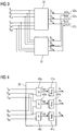
- FIG. 4 shows an example of an embodiment of the differential protection unit 30.
- the differential protection unit 30 is supplied on the input side with the current values I a1 , I a2 , I a3 or I b1 , I b2 and I b3 .
- the respectively Current values assigned to a phase of the protected object are supplied to difference value formers 40a, 40b and 40c, where, according to equation (1), an absolute sum of the current values is formed for the respective phase: I diff .
- the differential protection unit 30 On the output side, the differential protection unit 30 outputs trip signals A 1 , A 2 and A 3 , if for the respective phase of the respective differential current value I diff, 1 , I diff, 2 or I diff, 3 above in the thresholds 41a, 41b, 41c for Comparison used thresholds.
- FIG. 5 shows a first embodiment of a blocking device 50.
- the blocking means 50 are supplied with the individual current values I a1 , I a2 , I a3 and I b1 , I b2 , I b3 .
- the respective current values belonging to one phase are supplied on the input side to summation formers 51a, 51b, 51c, which according to equation (2) below the stabilizing current values belonging to the corresponding phase as the sum of the amounts of the individual current values.
- I stab, i is the stabilizing current of the respective phase; the remaining terms are to be understood according to equation (1).
- the resulting stabilization current values I bar, I, I bar, 2 and I bar, 3 are output on the output side of the summation devices 51 a, 51 b and 51 c to a maximum detection device 52.
- the maximum detection device 52 considers the individual stabilization current values I bar , 1 , I bar, 2 and I bar, 3 and determines therefrom the maximum stabilization current value I bar , max which is output by the maximum detection device 52 on the output side.
- the maximum stabilization current value I stab, max is supplied to a threshold value element 53 and serves there for the dynamic, that is adapted to the maximum stabilization current value I stab, max , determination of a stabilization threshold value.
- the stabilization current value I stab, max is multiplied by a transverse stabilization factor f, wherein the transverse stabilization factor f can be selected in the range between 0 and 1.
- Usual suitable values for the transverse stabilization factor f are between 0.3 and 0.5, preferably a value of 0.4 is selected.
- the threshold value element 53 is also supplied on the input side with the stabilization current values I bar, I, I bar, 2 and I bar, 3 .
- the stabilization current values I bar , 1 , I bar, 2 and I bar, 3 are compared with the stabilization threshold value f ⁇ I stab, max and it becomes for that phase a blocking signal B 1 , B 2 , B 3 output on the output side, whose stabilizing current value I bar , 1 , I bar, 2 , I bar , 3 the stabilization threshold f stab I , max below.
- This manner of forming the blocking signal B 1 , B 2 , B 3 is based on the fact that a rise in the stabilizing current of a stabilization current not affected by a short circuit is significantly less than the stabilizing current I stab, max that is actually generated by influencing the current transformers phase affected by the short circuit.
- the transverse stabilization factor f thus designates the percentage of the maximum stabilizing current I stab, max , which does not exceed a rise in the stabilizing current value of a specific phase, which is generated merely by influencing the current transformers (ie, as it were, by a transverse influencing).
- the blocking device 50 recognizes on the basis of the current values I a2 and I b2 with respect to this phase 13b stabilizing current value I bar , 2 compared to the other lower failing stabilizing current values I bar , 1 and I bar, 3 the maximum stabilizing current value I bar , max , which is multiplied by the transverse stabilization factor f.
- the stabilization current values formed from the current values I a1, I b1 and I a3 and I b3 I bar, 1, and I rod, 3 should normally be increased only by influencing the current transformer and, therefore, not exceed the stabilizing threshold value in the threshold member 53, so that for these phases, the blocking signals B 1 and B 3 are generated while the blocking signal B 2 is not generated because of the associated phase 13 b, the maximum stabilizing current value I bar , max has been detected.
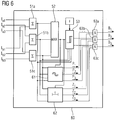
- FIG. 2 shows a second exemplary embodiment of a blocking device 60, which essentially corresponds to the first exemplary embodiment of the blocking device 50. Therefore, corresponding components of the Embodiments according to the Figures 5 and 6 marked with corresponding reference numerals.
- the blocking unit 60 In order to further increase the reliability of the formation of the blocking signals B 1 , B 2 and B 3 , the blocking unit 60 according to FIG. 6 in addition, a phase position detection device 61 and a time offset detection device 62 are provided.
- the phase angle detection device 61 is the input side of the output from the sum generators 51a, 51b, 51c output phase-related stabilization current values I bar , 1 , I bar, 2 and I bar, 3 acted upon. In addition, the phase angle detection device 61 is supplied with the maximum stabilization current value I stab, max .
- the phase position detection device 61 compares the phase positions of the individual stabilizing current values I bar, I, I bar, 2 , I bar, 3 with the phase position of the maximum stabilizing current value I bar , max and then then outputs a phase position output signal P 1 , P 2 , P for the corresponding phase 3 , when the phase position of the stabilizing current of the relevant phase of the phase position of the maximum stabilizing current I bar , max corresponds or is exactly shifted by 180 °.
- the phase-position signals P 1 , P 2 , P 3 are supplied to AND gates 63a, 63b and 63c, to which the output signals of the threshold value element 53 are supplied on the input side.
- phase position detection device 61 the knowledge is applied that when influenced by the current transformer to each other resulting increased stabilization current values whose phase position is impressed by the short-circuit current on the primary side of the respective affected by the short circuit phase.
- the time offset detection device 62 is also supplied with the maximum stabilization current value I stab, max .
- the skew detection means 62 examines the gradients Immediately successive values of the phase-related stabilization current values I bar , 1 , I bar, 2 , I bar, 3 and the maximum stabilization current value I stab, max and gives exactly a time offset signal Z 1 , Z 2 , Z 3 for a relevant phase, if an increase in the course of the stabilization current values I bar , 1 , I bar, 2 , I bar, 3 for the relevant phase with a specific time offset, preferably with a time offset between 2 and 3 milliseconds, to the increase in the course of the maximum stabilization current values I stab, max occurs.
- the corresponding time offset signal Z 1 , Z 2 , Z 3 is also supplied to the AND gates 63a, 63b, 63c
- the AND gates 63a, 63b and 63c emit a blocking signal if and only if all input conditions are met, that is, if the stabilization current value of a particular phase is below the stabilization threshold, the phase of the stabilization current of that phase coincides with the phase of the maximum stabilization current and the increase of the stabilization current profile of the relevant phase follows the rise of the maximum stabilization current profile by a specific time offset.
- phase comparator 61 and the time offset detection means 62 are shown, in the scope of the invention, such embodiments are also conceivable in which additionally either only the phase offset detection means 61 or the time offset detection means 62 is present.
- the blocking signals B 1 , B 2 , B 3 are then formed according to two input criteria.
- the blocking device 60 may differ from the illustration according to FIG. 6 It may also be provided that the differential current values are supplied to the phase position detection device 61 and the time offset detection device 62 instead of the stabilization current values and these are compared with the phase position or the profile of the difference current values of that phase with the maximum stabilization current value.
- the invention thus provides a total of a method that can be easily included in the software of differential protection devices to avoid by triggering the current transformer caused false triggering. With the described method can be detected in a reliable manner by influencing the current transformer with each other resulting differential currents and generation of corresponding trigger signals can be prevented.
- the criteria for forming the blocking signals it is also possible to prevent a false blocking of a triggering signal if there is actually a short circuit for a particular phase, that is to say if two or three phases are actually affected by a short circuit instead of a single phase.
- the checks of the criteria for the actually affected by the short circuit phases exceeding the stabilization threshold and optionally a deviating from zero or 180 ° phase position offset and falls below the time offset since in this case does not prevail the influence of the current transformers with each other, but the high short-circuit actually applied to the respective primary side of the individual current transformers influences the value of the differential currents or stabilizing currents.
Landscapes
- Engineering & Computer Science (AREA)
- Power Engineering (AREA)
- Emergency Protection Circuit Devices (AREA)
Claims (7)
- Procédé de détection d'un court-circuit concernant au moins une phase (13a, 13b, 13c) d'un objet (11) à protéger dans un réseau de transport d'énergie électrique polyphasé, dans lequel- on détecte, pour chaque phase (13a, 13b, 13c), des valeurs de courant en au moins deux points de mesure de l'objet (11) à protéger;- pour chaque phase (13a, 13b, 13c), on détermine des valeurs de courant de différence à partir des valeurs de courant et- on produit un signal de déclenchement pour une phase (par exemple 13b) déterminée si la valeur de courant de différence de cette phase (par exemple 13b) dépasse une valeur de seuil;dans lequel- pour chaque phase (13a, 13b, 13c), on détermine, à partir des valeurs de courant, une valeur de courant de stabilisation et on produit un signal de blocage pour une phase (par exemple 13a, 13c) déterminée si la valeur de courant de stabilisation concernée est inférieure à une valeur de seuil de stabilisation donnée à l'avance, le signal de blocage supprimant l'émission d'un signal de déclenchement pour la phase (par exemple 13a, 13c) concernée,caractérisé en ce que- on détermine la valeur de courant de stabilisation maximum et on fixe la valeur de seuil de stabilisation en fonction de la valeur de courant de stabilisation maximum;- on détermine une position en phase entre les valeurs de courant de différence ou les valeurs de courant de stabilisation de la phase (par exemple 13b) ayant le courant de stabilisation maximum et les valeurs de courant de différence ou les valeurs de courant de stabilisation des autres phases (par exemple 13a, 13c) et- on ne produit le signal de blocage pour une phase (par exemple (13a, 13c) déterminée que si la position en phase de cette phase (par exemple 13a, 13c) coïncide avec la position en phase de la phase (par exemple 13b) ayant la valeur de courant de stabilisation maximum ou est décalée de 180°.
- Procédé suivant la revendication 1,
caractérisé en ce que- l'on fixe la valeur de seuil de stabilisation en multipliant la valeur de courant de stabilisation maximum par un facteur de stabilisation transversale pouvant être donné à l'avance. - Procédé suivant la revendication 2,
caractérisé en ce que- l'on choisit le facteur de stabilisation transversale entre 0 et 1, de préférence entre 0,3 et 0,5. - Procédé suivant la revendication 3,
caractérisé en ce que- l'on choisit la valeur 0,4 comme facteur de stabilisation transversale. - Procédé suivant l'une des revendications précédents,
caractérisé en ce que- on considère pour chaque phase (13a, 13b, 13c) une courbe composée de plusieurs valeurs de courant de différence ou valeur de courant de stabilisation se succédant immédiatement dans le temps et- on ne produit un signal de blocage pour une phase (par exemple 13a, 13c) déterminée que si une croissance de la courbe pour cette phase (par exemple 13a, 13c) se produit seulement en étant retardée d'un décalage dans le temps donné à l'avance par rapport à la croissance de la courbe pour la phase (par exemple 13b) ayant la valeur de courant de stabilisation maximum. - Procédé suivant l'une des revendications précédentes,
caractérisé en ce que- on calcule les valeurs de courant de stabilisation respectives en sommant les valeurs absolues de toutes les valeurs de courant détectées pour les phases (13a, 13b, 13c) concernées. - Appareil (12a, 12b) électrique de protection différentielle pour contrôler des courts-circuits sur un objet (11) à protéger dans un réseau d'alimentation en énergie électrique comprenant- un dispositif de traitement de données, qui est conçu pour effectuer un procédé suivant l'une des revendications 1 à 6.
Applications Claiming Priority (1)
| Application Number | Priority Date | Filing Date | Title |
|---|---|---|---|
| PCT/EP2008/009190 WO2010048973A1 (fr) | 2008-10-28 | 2008-10-28 | Procédé de protection différentielle et appareil de protection différentielle |
Publications (2)
| Publication Number | Publication Date |
|---|---|
| EP2345123A1 EP2345123A1 (fr) | 2011-07-20 |
| EP2345123B1 true EP2345123B1 (fr) | 2018-11-28 |
Family
ID=40671073
Family Applications (1)
| Application Number | Title | Priority Date | Filing Date |
|---|---|---|---|
| EP08874999.9A Active EP2345123B1 (fr) | 2008-10-28 | 2008-10-28 | Procédé de protection différentielle et appareil de protection différentielle |
Country Status (4)
| Country | Link |
|---|---|
| EP (1) | EP2345123B1 (fr) |
| CN (1) | CN102204050B (fr) |
| BR (1) | BRPI0823146A2 (fr) |
| WO (1) | WO2010048973A1 (fr) |
Families Citing this family (5)
| Publication number | Priority date | Publication date | Assignee | Title |
|---|---|---|---|---|
| DE102009057633B3 (de) | 2009-12-09 | 2011-03-31 | Thyssenkrupp Presta Teccenter Ag | Verfahren zur Herstellung einer gebauten Nockenwelle, Nockenwellengrundkörper und gebaute Nockenwelle |
| CN103135023B (zh) * | 2011-11-28 | 2015-12-09 | 西门子公司 | 在电力网络中检测短路的方法和装置 |
| US20170138996A1 (en) * | 2014-03-28 | 2017-05-18 | Siemens Aktiengesellschaft | Differential protection method and differential protection device |
| CN110927508A (zh) * | 2019-12-30 | 2020-03-27 | 中铁建电气化局集团第一工程有限公司 | 一种便携式差动回路校验仪及校验方法 |
| CN114089250B (zh) * | 2021-10-11 | 2024-06-18 | 国电南瑞科技股份有限公司 | 一种电流互感器异常识别与处理方法 |
Family Cites Families (5)
| Publication number | Priority date | Publication date | Assignee | Title |
|---|---|---|---|---|
| SE470295B (sv) * | 1992-05-22 | 1994-01-10 | Asea Brown Boveri | Förfarande och anordning för att förhindra understabilisering av längsdifferentialskydd vid yttre fel och strömtransformatormättning |
| JPH11341679A (ja) * | 1998-05-25 | 1999-12-10 | Toshiba Corp | ディジタル形保護継電器 |
| JP3768441B2 (ja) * | 2001-12-25 | 2006-04-19 | 三菱電機株式会社 | 母線保護リレ− |
| US7199991B2 (en) * | 2002-06-27 | 2007-04-03 | Nxt Phase T & D Corporation | Electrical bus protection method & apparatus |
| JP2004088919A (ja) * | 2002-08-27 | 2004-03-18 | Kansai Electric Power Co Inc:The | 電流差動保護継電装置 |
-
2008
- 2008-10-28 EP EP08874999.9A patent/EP2345123B1/fr active Active
- 2008-10-28 WO PCT/EP2008/009190 patent/WO2010048973A1/fr not_active Ceased
- 2008-10-28 BR BRPI0823146-0A patent/BRPI0823146A2/pt not_active IP Right Cessation
- 2008-10-28 CN CN200880131714.9A patent/CN102204050B/zh not_active Expired - Fee Related
Non-Patent Citations (1)
| Title |
|---|
| None * |
Also Published As
| Publication number | Publication date |
|---|---|
| WO2010048973A1 (fr) | 2010-05-06 |
| EP2345123A1 (fr) | 2011-07-20 |
| RU2011121565A (ru) | 2012-12-10 |
| CN102204050A (zh) | 2011-09-28 |
| CN102204050B (zh) | 2014-06-18 |
| BRPI0823146A2 (pt) | 2015-06-16 |
Similar Documents
| Publication | Publication Date | Title |
|---|---|---|
| EP3198698B1 (fr) | Procédé de protection de différentiel et appareil de protection de différentiel permettant de mettre en oeuvre un procédé de protection de différentiel | |
| EP3447870B1 (fr) | Procédé de protection différentielle, dispositif de protection différentielle et système de protection différentielle | |
| DE69823936T2 (de) | Erdschlussfehlerschutzschaltung für mehrquellensystem | |
| EP2605352B1 (fr) | Protection de lignes parallèles d'un réseau d'alimentation en énergie électrique | |
| DE112018005677T5 (de) | Verfahren und vorrichtung zur fehlererkennung und zum schutz von elektrischen netzwerken | |
| EP3300199B1 (fr) | Procédé et dispositif destinés à contrôler un disjoncteur pour un réseau d'alimentation en énergie électrique lors du passage à zéro du courant | |
| EP3552289B1 (fr) | Disjoncteur basse tension | |
| CH697108A5 (de) | Verfahren zur Detektion eines Fehlers auf Übertragungsleitungen unter Verwendung von Harmonischen und einem Zustandsübergangsdiagramm. | |
| EP2345123B1 (fr) | Procédé de protection différentielle et appareil de protection différentielle | |
| EP3876373A1 (fr) | Procédé de protection différentielle, dispositif de protection différentielle et système de protection différentielle | |
| EP3108554B1 (fr) | Procédé de protection de différentiel et dispositif de protection de différentiel | |
| EP1416287B1 (fr) | Procédé permettant de produire un signal d'erreur indiquant le court-circuit avec la terre | |
| WO2015028062A1 (fr) | Procédé de protection différentielle et appareil de protection différentielle permettant la mise en œuvre d'un tel procédé | |
| DE2604311A1 (de) | Phasenvergleichsrelais | |
| EP3207610B1 (fr) | Procédé et dispositif de protection pour générer un signal de défaut indiquant un type de défaut d'un réseau d'alimentation en énergie électrique polyphasée | |
| WO2008034400A1 (fr) | Procédé pour générer un signal d'erreur indiquant la présence d'une erreur dans un circuit électrique de transformateur de courant auxiliaire, ainsi que dispositif de protection par circuit de compensation | |
| DE102018128121A1 (de) | AC/DC-Umwandlungs-Anordnung | |
| EP3868021B1 (fr) | Commutateur électronique | |
| EP2901534B1 (fr) | Procédé de protection différentielle et appareil de protection servant à mettre en uvre un procédé de protection différentielle | |
| EP3595114B1 (fr) | Procédé et agencement de détection d'une erreur de spire dans un transformateur sur la base de valeurs correspondantes de courant à séquence inverse | |
| DE69122078T2 (de) | Leistungseinführungssystem | |
| DE4026799A1 (de) | Verfahren zur selektiven erfassung von fehlern der leiter in hoch- und hoechstspannungsnetzen | |
| EP1977492A1 (fr) | Dispositif de protection comprenant un commutateur de puissance, notamment un commutateur de puissance à basse tension | |
| DE102004008994B4 (de) | Verfahren und Schaltungsanordnung zur Fehlerdiagnose in Hochspannungsnetzen | |
| DE2736953A1 (de) | Phasenvergleichsschutzschalteinrichtung |
Legal Events
| Date | Code | Title | Description |
|---|---|---|---|
| PUAI | Public reference made under article 153(3) epc to a published international application that has entered the european phase |
Free format text: ORIGINAL CODE: 0009012 |
|
| 17P | Request for examination filed |
Effective date: 20110420 |
|
| AK | Designated contracting states |
Kind code of ref document: A1 Designated state(s): AT BE BG CH CY CZ DE DK EE ES FI FR GB GR HR HU IE IS IT LI LT LU LV MC MT NL NO PL PT RO SE SI SK TR |
|
| AX | Request for extension of the european patent |
Extension state: AL BA MK RS |
|
| DAX | Request for extension of the european patent (deleted) | ||
| RAP1 | Party data changed (applicant data changed or rights of an application transferred) |
Owner name: SIEMENS AKTIENGESELLSCHAFT |
|
| RAP1 | Party data changed (applicant data changed or rights of an application transferred) |
Owner name: SIEMENS AKTIENGESELLSCHAFT |
|
| GRAP | Despatch of communication of intention to grant a patent |
Free format text: ORIGINAL CODE: EPIDOSNIGR1 |
|
| STAA | Information on the status of an ep patent application or granted ep patent |
Free format text: STATUS: GRANT OF PATENT IS INTENDED |
|
| INTG | Intention to grant announced |
Effective date: 20180626 |
|
| RIN1 | Information on inventor provided before grant (corrected) |
Inventor name: FUNK, HANS-WERNER Inventor name: SCHNEIDER, SEBASTIAN Inventor name: SCHICK, MATHIAS Inventor name: SCHUMACHER, MARTIN Inventor name: SCHAEFER, BERND |
|
| GRAS | Grant fee paid |
Free format text: ORIGINAL CODE: EPIDOSNIGR3 |
|
| GRAA | (expected) grant |
Free format text: ORIGINAL CODE: 0009210 |
|
| STAA | Information on the status of an ep patent application or granted ep patent |
Free format text: STATUS: THE PATENT HAS BEEN GRANTED |
|
| AK | Designated contracting states |
Kind code of ref document: B1 Designated state(s): AT BE BG CH CY CZ DE DK EE ES FI FR GB GR HR HU IE IS IT LI LT LU LV MC MT NL NO PL PT RO SE SI SK TR |
|
| REG | Reference to a national code |
Ref country code: GB Ref legal event code: FG4D Free format text: NOT ENGLISH |
|
| REG | Reference to a national code |
Ref country code: CH Ref legal event code: EP |
|
| REG | Reference to a national code |
Ref country code: AT Ref legal event code: REF Ref document number: 1071356 Country of ref document: AT Kind code of ref document: T Effective date: 20181215 |
|
| REG | Reference to a national code |
Ref country code: DE Ref legal event code: R096 Ref document number: 502008016494 Country of ref document: DE |
|
| REG | Reference to a national code |
Ref country code: IE Ref legal event code: FG4D Free format text: LANGUAGE OF EP DOCUMENT: GERMAN |
|
| REG | Reference to a national code |
Ref country code: NL Ref legal event code: MP Effective date: 20181128 |
|
| REG | Reference to a national code |
Ref country code: LT Ref legal event code: MG4D |
|
| PG25 | Lapsed in a contracting state [announced via postgrant information from national office to epo] |
Ref country code: HR Free format text: LAPSE BECAUSE OF FAILURE TO SUBMIT A TRANSLATION OF THE DESCRIPTION OR TO PAY THE FEE WITHIN THE PRESCRIBED TIME-LIMIT Effective date: 20181128 Ref country code: LT Free format text: LAPSE BECAUSE OF FAILURE TO SUBMIT A TRANSLATION OF THE DESCRIPTION OR TO PAY THE FEE WITHIN THE PRESCRIBED TIME-LIMIT Effective date: 20181128 Ref country code: LV Free format text: LAPSE BECAUSE OF FAILURE TO SUBMIT A TRANSLATION OF THE DESCRIPTION OR TO PAY THE FEE WITHIN THE PRESCRIBED TIME-LIMIT Effective date: 20181128 Ref country code: NO Free format text: LAPSE BECAUSE OF FAILURE TO SUBMIT A TRANSLATION OF THE DESCRIPTION OR TO PAY THE FEE WITHIN THE PRESCRIBED TIME-LIMIT Effective date: 20190228 Ref country code: ES Free format text: LAPSE BECAUSE OF FAILURE TO SUBMIT A TRANSLATION OF THE DESCRIPTION OR TO PAY THE FEE WITHIN THE PRESCRIBED TIME-LIMIT Effective date: 20181128 Ref country code: BG Free format text: LAPSE BECAUSE OF FAILURE TO SUBMIT A TRANSLATION OF THE DESCRIPTION OR TO PAY THE FEE WITHIN THE PRESCRIBED TIME-LIMIT Effective date: 20190228 Ref country code: IS Free format text: LAPSE BECAUSE OF FAILURE TO SUBMIT A TRANSLATION OF THE DESCRIPTION OR TO PAY THE FEE WITHIN THE PRESCRIBED TIME-LIMIT Effective date: 20190328 Ref country code: FI Free format text: LAPSE BECAUSE OF FAILURE TO SUBMIT A TRANSLATION OF THE DESCRIPTION OR TO PAY THE FEE WITHIN THE PRESCRIBED TIME-LIMIT Effective date: 20181128 |
|
| PG25 | Lapsed in a contracting state [announced via postgrant information from national office to epo] |
Ref country code: GR Free format text: LAPSE BECAUSE OF FAILURE TO SUBMIT A TRANSLATION OF THE DESCRIPTION OR TO PAY THE FEE WITHIN THE PRESCRIBED TIME-LIMIT Effective date: 20190301 Ref country code: PT Free format text: LAPSE BECAUSE OF FAILURE TO SUBMIT A TRANSLATION OF THE DESCRIPTION OR TO PAY THE FEE WITHIN THE PRESCRIBED TIME-LIMIT Effective date: 20190328 Ref country code: SE Free format text: LAPSE BECAUSE OF FAILURE TO SUBMIT A TRANSLATION OF THE DESCRIPTION OR TO PAY THE FEE WITHIN THE PRESCRIBED TIME-LIMIT Effective date: 20181128 |
|
| PG25 | Lapsed in a contracting state [announced via postgrant information from national office to epo] |
Ref country code: NL Free format text: LAPSE BECAUSE OF FAILURE TO SUBMIT A TRANSLATION OF THE DESCRIPTION OR TO PAY THE FEE WITHIN THE PRESCRIBED TIME-LIMIT Effective date: 20181128 |
|
| PG25 | Lapsed in a contracting state [announced via postgrant information from national office to epo] |
Ref country code: PL Free format text: LAPSE BECAUSE OF FAILURE TO SUBMIT A TRANSLATION OF THE DESCRIPTION OR TO PAY THE FEE WITHIN THE PRESCRIBED TIME-LIMIT Effective date: 20181128 Ref country code: DK Free format text: LAPSE BECAUSE OF FAILURE TO SUBMIT A TRANSLATION OF THE DESCRIPTION OR TO PAY THE FEE WITHIN THE PRESCRIBED TIME-LIMIT Effective date: 20181128 Ref country code: CZ Free format text: LAPSE BECAUSE OF FAILURE TO SUBMIT A TRANSLATION OF THE DESCRIPTION OR TO PAY THE FEE WITHIN THE PRESCRIBED TIME-LIMIT Effective date: 20181128 |
|
| REG | Reference to a national code |
Ref country code: DE Ref legal event code: R097 Ref document number: 502008016494 Country of ref document: DE |
|
| PG25 | Lapsed in a contracting state [announced via postgrant information from national office to epo] |
Ref country code: SK Free format text: LAPSE BECAUSE OF FAILURE TO SUBMIT A TRANSLATION OF THE DESCRIPTION OR TO PAY THE FEE WITHIN THE PRESCRIBED TIME-LIMIT Effective date: 20181128 Ref country code: EE Free format text: LAPSE BECAUSE OF FAILURE TO SUBMIT A TRANSLATION OF THE DESCRIPTION OR TO PAY THE FEE WITHIN THE PRESCRIBED TIME-LIMIT Effective date: 20181128 Ref country code: RO Free format text: LAPSE BECAUSE OF FAILURE TO SUBMIT A TRANSLATION OF THE DESCRIPTION OR TO PAY THE FEE WITHIN THE PRESCRIBED TIME-LIMIT Effective date: 20181128 |
|
| PLBE | No opposition filed within time limit |
Free format text: ORIGINAL CODE: 0009261 |
|
| STAA | Information on the status of an ep patent application or granted ep patent |
Free format text: STATUS: NO OPPOSITION FILED WITHIN TIME LIMIT |
|
| PG25 | Lapsed in a contracting state [announced via postgrant information from national office to epo] |
Ref country code: SI Free format text: LAPSE BECAUSE OF FAILURE TO SUBMIT A TRANSLATION OF THE DESCRIPTION OR TO PAY THE FEE WITHIN THE PRESCRIBED TIME-LIMIT Effective date: 20181128 |
|
| 26N | No opposition filed |
Effective date: 20190829 |
|
| PG25 | Lapsed in a contracting state [announced via postgrant information from national office to epo] |
Ref country code: TR Free format text: LAPSE BECAUSE OF FAILURE TO SUBMIT A TRANSLATION OF THE DESCRIPTION OR TO PAY THE FEE WITHIN THE PRESCRIBED TIME-LIMIT Effective date: 20181128 |
|
| PG25 | Lapsed in a contracting state [announced via postgrant information from national office to epo] |
Ref country code: MC Free format text: LAPSE BECAUSE OF FAILURE TO SUBMIT A TRANSLATION OF THE DESCRIPTION OR TO PAY THE FEE WITHIN THE PRESCRIBED TIME-LIMIT Effective date: 20181128 |
|
| REG | Reference to a national code |
Ref country code: CH Ref legal event code: PL |
|
| PG25 | Lapsed in a contracting state [announced via postgrant information from national office to epo] |
Ref country code: CH Free format text: LAPSE BECAUSE OF NON-PAYMENT OF DUE FEES Effective date: 20191031 Ref country code: LI Free format text: LAPSE BECAUSE OF NON-PAYMENT OF DUE FEES Effective date: 20191031 Ref country code: LU Free format text: LAPSE BECAUSE OF NON-PAYMENT OF DUE FEES Effective date: 20191028 |
|
| REG | Reference to a national code |
Ref country code: BE Ref legal event code: MM Effective date: 20191031 |
|
| PG25 | Lapsed in a contracting state [announced via postgrant information from national office to epo] |
Ref country code: BE Free format text: LAPSE BECAUSE OF NON-PAYMENT OF DUE FEES Effective date: 20191031 |
|
| PG25 | Lapsed in a contracting state [announced via postgrant information from national office to epo] |
Ref country code: IE Free format text: LAPSE BECAUSE OF NON-PAYMENT OF DUE FEES Effective date: 20191028 |
|
| REG | Reference to a national code |
Ref country code: AT Ref legal event code: MM01 Ref document number: 1071356 Country of ref document: AT Kind code of ref document: T Effective date: 20191028 |
|
| PG25 | Lapsed in a contracting state [announced via postgrant information from national office to epo] |
Ref country code: AT Free format text: LAPSE BECAUSE OF NON-PAYMENT OF DUE FEES Effective date: 20191028 |
|
| PG25 | Lapsed in a contracting state [announced via postgrant information from national office to epo] |
Ref country code: CY Free format text: LAPSE BECAUSE OF FAILURE TO SUBMIT A TRANSLATION OF THE DESCRIPTION OR TO PAY THE FEE WITHIN THE PRESCRIBED TIME-LIMIT Effective date: 20181128 |
|
| PG25 | Lapsed in a contracting state [announced via postgrant information from national office to epo] |
Ref country code: HU Free format text: LAPSE BECAUSE OF FAILURE TO SUBMIT A TRANSLATION OF THE DESCRIPTION OR TO PAY THE FEE WITHIN THE PRESCRIBED TIME-LIMIT; INVALID AB INITIO Effective date: 20081028 Ref country code: MT Free format text: LAPSE BECAUSE OF FAILURE TO SUBMIT A TRANSLATION OF THE DESCRIPTION OR TO PAY THE FEE WITHIN THE PRESCRIBED TIME-LIMIT Effective date: 20181128 |
|
| PGFP | Annual fee paid to national office [announced via postgrant information from national office to epo] |
Ref country code: GB Payment date: 20251111 Year of fee payment: 18 |
|
| PGFP | Annual fee paid to national office [announced via postgrant information from national office to epo] |
Ref country code: IT Payment date: 20251027 Year of fee payment: 18 |
|
| PGFP | Annual fee paid to national office [announced via postgrant information from national office to epo] |
Ref country code: FR Payment date: 20251020 Year of fee payment: 18 |
|
| PGFP | Annual fee paid to national office [announced via postgrant information from national office to epo] |
Ref country code: DE Payment date: 20251219 Year of fee payment: 18 |