EP2348366A1 - Feuille conductrice de rouleau de charge, et cartouche de révélateur - Google Patents
Feuille conductrice de rouleau de charge, et cartouche de révélateur Download PDFInfo
- Publication number
- EP2348366A1 EP2348366A1 EP09827166A EP09827166A EP2348366A1 EP 2348366 A1 EP2348366 A1 EP 2348366A1 EP 09827166 A EP09827166 A EP 09827166A EP 09827166 A EP09827166 A EP 09827166A EP 2348366 A1 EP2348366 A1 EP 2348366A1
- Authority
- EP
- European Patent Office
- Prior art keywords
- contact plate
- conductive film
- charge roller
- developer cartridge
- input
- Prior art date
- Legal status (The legal status is an assumption and is not a legal conclusion. Google has not performed a legal analysis and makes no representation as to the accuracy of the status listed.)
- Withdrawn
Links
Images


Classifications
-
- G—PHYSICS
- G03—PHOTOGRAPHY; CINEMATOGRAPHY; ANALOGOUS TECHNIQUES USING WAVES OTHER THAN OPTICAL WAVES; ELECTROGRAPHY; HOLOGRAPHY
- G03G—ELECTROGRAPHY; ELECTROPHOTOGRAPHY; MAGNETOGRAPHY
- G03G21/00—Arrangements not provided for by groups G03G13/00 - G03G19/00, e.g. cleaning, elimination of residual charge
- G03G21/16—Mechanical means for facilitating the maintenance of the apparatus, e.g. modular arrangements
- G03G21/18—Mechanical means for facilitating the maintenance of the apparatus, e.g. modular arrangements using a processing cartridge, whereby the process cartridge comprises at least two image processing means in a single unit
- G03G21/1839—Means for handling the process cartridge in the apparatus body
- G03G21/1867—Means for handling the process cartridge in the apparatus body for electrically connecting the process cartridge to the apparatus, electrical connectors, power supply
-
- G—PHYSICS
- G03—PHOTOGRAPHY; CINEMATOGRAPHY; ANALOGOUS TECHNIQUES USING WAVES OTHER THAN OPTICAL WAVES; ELECTROGRAPHY; HOLOGRAPHY
- G03G—ELECTROGRAPHY; ELECTROPHOTOGRAPHY; MAGNETOGRAPHY
- G03G2221/00—Processes not provided for by group G03G2215/00, e.g. cleaning or residual charge elimination
- G03G2221/16—Mechanical means for facilitating the maintenance of the apparatus, e.g. modular arrangements and complete machine concepts
- G03G2221/1693—Mechanical means for facilitating the maintenance of the apparatus, e.g. modular arrangements and complete machine concepts for charging
Definitions
- the present invention relates to a charge roller conductive film used in an image forming apparatus developer cartridge and a developer cartridge having the conductive film.
- the present invention is based on Chinese Utility Model Patent Application Number 200820203938.3, filed on Nov. 19, 2008 . The contents of the application are incorporated herein as a reference.
- a developer cartridge used in a laser printer and other image forming apparatus are generally divided into two types: an all-in-one cartridge and a split cartridge.
- the all-in-one cartridge is formed by a combination of a developing unit and a processing unit permanently connected to each other, and is used as one assembled inside the laser printer.
- the split cartridge refers to a developer cartridge in which the above developing unit and processing unit can relatively be removed by a user, and the developing unit can be individually replaced.
- the developing unit mainly comprises a developing unit frame, a developer chamber, an agitator, a toner supply roller, a developing roller and a toner deposit blade. The agitator, the toner supply roller and the developing roller can be rotatably assembled on the developing unit frame.
- the processing unit mainly comprises a processing unit frame, a waste toner chamber, a photosensitive drum, a charge roller and a cleaning blade.
- the photosensitive drum and the charge roller can be rotatably assembled on the processing unit frame.
- the developer chamber provides a developer storage space and an appropriate developer transmission channel;
- the agitator can make a stand-by developer exported to the developing roller to be uniformly distributed through its own rotation;
- the developing roller adjacent to the photosensitive drum makes the developer to be adsorbed to the electrostatic latent image region on the photosensitive drum through the role of opposite polarity charge.
- the charge roller of the processing unit provides charging to the photosensitive drum causing the photosensitive area of the photosensitive drum to carry the charge with the opposite polarity to the developer's adsorbed charge.
- the cleaning blade can frictionally contact with the photosensitive area's surface of the photosensitive drum through visual image transfer and scrape the remained developer on the photosensitive area's surface of the photosensitive drum into the waste toner chamber.
- Chinese Utility Model Patent Number CN2755647Y discloses a developer cartridge that can be removably mounted on a main assembly of an electrophotographic image forming apparatus.
- the specification of the patent describes the overall structure of the developer cartridge in detail.
- the main assembly comprises an output contact movable between an electrical connection position and a retracted position, a mobile member used for moving the output contact, and a flexible function member used for flexibly pushing the mobile member toward the retracted position to push the output contact.
- the developer cartridge comprises an electrophotographic photosensitive drum, a processing device acted on the photosensitive drum and a movable operational member moved relative to the developer cartridge's frame, in which the movable operational member can connect with a permanent connecting member and move relative to the cartridge frame when the developer cartridge is inserted into the apparatus main assembly. And after said connection, the movable operational member can connect with the movable connecting section of the mobile member to make the output contact to move from the retracted position to the electrical connection position by overcoming the elastic force. An input electrical contact is used to receive the connection via the output contact moved to the electrical connection position to start the processing device's voltage.
- the developer cartridge uses too many electrical connection accessories with complex structures. Thus, the use of a large number of molds is required, its production procedure is so long, and the product assembly process is relatively long and complex.
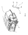
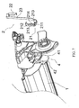
- an existing developer cartridge 1' is formed by a combination of a developing unit 2' and a processing unit 3' connected to each other.
- the frame of the processing unit 3' provides a conductive film 4' and a conductive film bearing 5' at one longitudinal end of a charge roller inside the processing unit 3' (not shown).
- the conductive film bearing 5' extends downward to form a bearing plate 6'.
- the bearing plate 6' has a left side and a right side parallel to each other, and a bottom perpendicular to the above two sides. The width of the bottom is the thickness of the bearing plate 6'.
- the conductive film 4' has an input 41', an output 42' and a transmission section 43' connecting the input 41' and the output 42'.
- the input 41' is electrically connected to the output 42' through the transmission section 43' and connected to the charge roller in order to provide pre-charged bias for the charge roller.
- the input 41' has a middle contact plate 44' shaped like a bent strip. The middle contact plate 44' comes in close contact with the bottom of the bearing plate 6'.
- the conductive film bearing 5' and the bearing plate 6' formed from its extension are existed in a naked and permanent state.
- An electrical contact of the image forming apparatus main assembly is also existed in a permanent state.
- the middle contact plate 44' of the conductive film 4' can contact with the electrical contact 7' of the image forming apparatus main assembly in its permanent position state to achieve the electrical connection without other extra accessories thereby reducing the complexity of device structure and helping to improve the stability of electrical contact.
- the conductive film 4' wraps the bearing plate 6' in a single side and contacts the electrical contact 7' only through the middle contact plate 44' with smaller width
- the electrical contact 7' suitable for the developer cartridge in the image forming apparatus main assembly is usually a thin and long metal wire with much smaller width
- the scenario in which the electrical contact 7' offsets toward both sides of the middle contact plate 44' as shown in Figure 4 and Figure 5 can occur when the developer cartridge is assembled inside the image forming apparatus main assembly and assembled in place.
- the phenomenon of bad contact with the middle contact plate 44' occurs.
- the image forming apparatus main assembly cannot induce the developer cartridge.
- the primary object of the present invention is to provide a charge roller conductive film having a good contact with an electrical contact of an image forming apparatus main assembly and reliable induction.
- Another object of the present invention is to provide a developer cartridge having the above charge roller conductive film.
- the present invention provides a charge roller conductive film comprising an input contacting an electrical contact of the image forming apparatus main assembly, an output connecting with a charge roller and a transmission section connecting with the input and the output.
- the input has a middle contact plate shaped like a bent strip. At least one side of said middle contact plate forms a side contact plate.
- both sides of a middle contact plate form a side contact plate so that regardless of which side of the electrical contact offsets the middle contact plate it can form a contact with side contact plate.
- at least one protrusion can be provided in the outer side of the side contact plate.
- Said side contact plate and said middle contact plate are best configured to be an integrated structure.
- Said side contact plate has two pieces in each side of said middle contact plate. Each piece of the side contact plate is roughly trapezoidal.
- the present invention provides a developer cartridge having the above charge roller conductive film comprising a developing unit and a processing unit connected to each other.
- Said processing unit comprises a processing unit frame, a photosensitive drum and a charge roller rotatably assembled on the processing unit frame.
- Said processing unit frame provides a charge roller conductive film and a conductive bearing plate at one longitudinal end of the charge roller.
- Said charge roller conductive film comprises an input fixed on said conductive bearing plate and contacting the electrical contact of the image forming apparatus main assembly, an output connecting with the charge roller, and a transmission section connecting with the input and the output.
- the input has a middle contact plate shaped like a bend strip. At least one side of said middle contact plate forms a side contact plate.
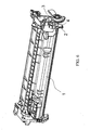
- the developer cartridge's main structure in the present invention is roughly similar as the developer cartridge as shown in Figure 1 .
- the main difference is the charge roller conductive film section.
- Figure 6 and Figure 7 only schematically show the processing unit 1 of the developer cartridge in the present invention but omit the developing unit and other parts identical to or similar as those in the existing technology, such as a photosensitive drum and a charge roller.
- the processing unit frame 1 provides a conductive film 2 and a conductive film bearing 3 at one longitudinal end (the axial direction of the charge roller).
- the conductive film bearing 3 extends downward to form a bearing plate 4.
- the bearing plate 4 has the left side and the right side 41 parallel to each other, and the bottom 42 perpendicular to the above two sides.
- the width of the bottom 42 is a thickness of the bearing plate 4.
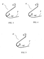
- the conductive film 2 has an input 21, an output 22 and a transmission section 23 connecting the input 21 and the output 22.
- the output 22 is electrically connected with the input 21 through the transmission section 23 and the charge roller so as to provide pre-charged bias to the charge roller.
- the input 21 has a middle contact plate 211 shaped like a bent strip. The middle contact plate 211 comes in close contact with the bottom 42 of the bearing plate 4 while clip 212 at both sides is used to wrap the entire input 21 and fix it on the bearing plate 4.
- two pieces of the side contact plates 213 are formed at two sides of the middle contact plate 211 in the above conductive film 2.
- Each piece of the side contact plate 213 is roughly trapezoidal and forms an integrated structure with the middle contact plate 211.
- the electrical contact 5 of the image forming apparatus main assembly is located whether below the middle of the conductive film 2 as shown in Figure 8 , or the left or right side offsetting the middle contact plate 211 as shown in Figure 9 and Figure 10 , the electrical contact 5 can form electrical connection with the conductive film 2 via contacting the middle contact plate 211 or the side contact plate 213.
- two small protrusions 214 are provided on the outer side of each piece of the side contact plate 213.
- the developer cartridge slides below into the corresponding positioning slot provided in the image forming apparatus main assembly along the chute on the side wall of the image forming apparatus main box.
- the position of the conductive film 2 is gradually reduced as the developer cartridge declines.
- the input 21 being wrapped around the outside surface of the bearing plate 4 by the conductive film 2 can also reach and contact the position of the electrical contact 5 of the image forming apparatus main assembly.
- the conductive film 2 of the developer cartridge can achieve electrical connection with the electrical contact 5 of the image forming apparatus main assembly.
- the side contact plate 213 on the conductive film 4 can only be provided at one side of the middle contact plate 211.
- the side contact plate 213 located at each side of the middle contact plate 211 can only have one piece, three pieces or more.
- the shape of each piece of the side contact plate 213 is not limited to trapezoidal but can be square, rectangular or any arbitrary shapes.
- each piece of the side contact plate 213 can also provide a structure form extending from the direction of the middle contact plate 211 far away from the middle contact plate 211 but is not limited to a substantially perpendicular structure form between the side contact plate 213 and the middle contact plate 211 shown in various embodiment drawings. Replacement program like this is in the protection range of the present invention.
- a conductive film in the present invention is added a side contact plate on at least one side of a middle contact plate.
Landscapes
- Engineering & Computer Science (AREA)
- Computer Vision & Pattern Recognition (AREA)
- Physics & Mathematics (AREA)
- General Physics & Mathematics (AREA)
- Electrophotography Configuration And Component (AREA)
- Electrostatic Charge, Transfer And Separation In Electrography (AREA)
Applications Claiming Priority (2)
| Application Number | Priority Date | Filing Date | Title |
|---|---|---|---|
| CNU2008202039383U CN201340516Y (zh) | 2008-11-19 | 2008-11-19 | 充电辊导电片和具有该导电片的显影剂盒 |
| PCT/CN2009/074907 WO2010057417A1 (fr) | 2008-11-19 | 2009-11-12 | Feuille conductrice de rouleau de charge, et cartouche de révélateur |
Publications (2)
| Publication Number | Publication Date |
|---|---|
| EP2348366A1 true EP2348366A1 (fr) | 2011-07-27 |
| EP2348366A4 EP2348366A4 (fr) | 2012-08-01 |
Family
ID=41236059
Family Applications (1)
| Application Number | Title | Priority Date | Filing Date |
|---|---|---|---|
| EP09827166A Withdrawn EP2348366A4 (fr) | 2008-11-19 | 2009-11-12 | Feuille conductrice de rouleau de charge, et cartouche de révélateur |
Country Status (4)
| Country | Link |
|---|---|
| US (1) | US8634739B2 (fr) |
| EP (1) | EP2348366A4 (fr) |
| CN (1) | CN201340516Y (fr) |
| WO (1) | WO2010057417A1 (fr) |
Families Citing this family (4)
| Publication number | Priority date | Publication date | Assignee | Title |
|---|---|---|---|---|
| CN201340516Y (zh) | 2008-11-19 | 2009-11-04 | 珠海天威飞马打印耗材有限公司 | 充电辊导电片和具有该导电片的显影剂盒 |
| CN201600555U (zh) * | 2009-12-24 | 2010-10-06 | 珠海天威飞马打印耗材有限公司 | 充电装置及感光鼓组件 |
| CN201600556U (zh) * | 2009-12-24 | 2010-10-06 | 珠海天威飞马打印耗材有限公司 | 充电装置及感光鼓组件 |
| JP2017167288A (ja) * | 2016-03-15 | 2017-09-21 | ブラザー工業株式会社 | 現像カートリッジ |
Family Cites Families (15)
| Publication number | Priority date | Publication date | Assignee | Title |
|---|---|---|---|---|
| JPH07219307A (ja) | 1994-01-27 | 1995-08-18 | Ricoh Co Ltd | 接触帯電装置及びその帯電部材の抵抗層形成方法 |
| JP3332813B2 (ja) * | 1997-08-01 | 2002-10-07 | キヤノン株式会社 | プロセスカートリッジ及び電子写真画像形成装置 |
| JP3697168B2 (ja) * | 2001-03-09 | 2005-09-21 | キヤノン株式会社 | プロセスカートリッジおよび電子写真画像形成装置 |
| US6922534B2 (en) * | 2001-12-28 | 2005-07-26 | Canon Kabushiki Kaisha | Process cartridge and electrophotographic image forming apparatus having electrical connection for memory |
| US6508601B1 (en) * | 2002-05-17 | 2003-01-21 | Monitek Electronics Limited | Charging contact plate |
| CN100454177C (zh) | 2003-09-30 | 2009-01-21 | 佳能株式会社 | 处理盒和电摄影成像设备 |
| JP4387934B2 (ja) * | 2003-12-09 | 2009-12-24 | キヤノン株式会社 | プロセスカートリッジ及び電子写真画像形成装置 |
| JP4035516B2 (ja) * | 2004-02-27 | 2008-01-23 | キヤノン株式会社 | 電子写真画像形成装置 |
| JP4639638B2 (ja) * | 2004-05-14 | 2011-02-23 | 富士ゼロックス株式会社 | 像形成ユニット |
| JP4689239B2 (ja) | 2004-11-12 | 2011-05-25 | キヤノン株式会社 | 画像形成装置 |
| CN2906694Y (zh) | 2006-05-09 | 2007-05-30 | 周茂柏 | 充电辊的支撑装置 |
| CN201035326Y (zh) | 2006-10-27 | 2008-03-12 | 刘江 | 一种打印机充电辊 |
| JP5212693B2 (ja) * | 2008-01-10 | 2013-06-19 | 株式会社リコー | 電子写真感光体、感光体支持装置、画像形成装置、およびプロセスカートリッジ |
| CN201340516Y (zh) | 2008-11-19 | 2009-11-04 | 珠海天威飞马打印耗材有限公司 | 充电辊导电片和具有该导电片的显影剂盒 |
| KR101080425B1 (ko) * | 2009-07-20 | 2011-11-04 | 삼성전자주식회사 | 현상기 및 이를 채용한 화상형성장치 |
-
2008
- 2008-11-19 CN CNU2008202039383U patent/CN201340516Y/zh not_active Expired - Lifetime
-
2009
- 2009-11-12 US US13/123,343 patent/US8634739B2/en not_active Expired - Fee Related
- 2009-11-12 EP EP09827166A patent/EP2348366A4/fr not_active Withdrawn
- 2009-11-12 WO PCT/CN2009/074907 patent/WO2010057417A1/fr not_active Ceased
Also Published As
| Publication number | Publication date |
|---|---|
| US20110243602A1 (en) | 2011-10-06 |
| CN201340516Y (zh) | 2009-11-04 |
| EP2348366A4 (fr) | 2012-08-01 |
| US8634739B2 (en) | 2014-01-21 |
| WO2010057417A1 (fr) | 2010-05-27 |
Similar Documents
| Publication | Publication Date | Title |
|---|---|---|
| JP4359854B2 (ja) | プロセスユニットおよび画像形成装置 | |
| US7248810B2 (en) | Cartridge, process cartridge, and electrophotographic image forming apparatus | |
| US20130183058A1 (en) | Image forming apparatus | |
| JP5126268B2 (ja) | 現像カートリッジ | |
| CN102073251B (zh) | 供电装置和图像形成设备 | |
| JP6331646B2 (ja) | 画像形成装置 | |
| CN105573079B (zh) | 薄片体提供装置及图像形成装置 | |
| CN102636972B (zh) | 充电装置、使用该充电装置的图像形成组件和图像形成设备 | |
| CN104090471B (zh) | 激光打印机 | |
| US8634739B2 (en) | Charge roller conductive film and developer cartridge | |
| US8744300B2 (en) | Image forming apparatus | |
| JP5353936B2 (ja) | 画像形成装置 | |
| JP6391272B2 (ja) | ローラ部材、ローラ支持機構、および画像形成装置 | |
| JP4893769B2 (ja) | 像担持体カートリッジ、プロセスカートリッジおよび画像形成装置 | |
| CN201069516Y (zh) | 一种改进的碳粉盒 | |
| US9471010B2 (en) | Developing device having regulating portions that regulate movement of a seal member | |
| CN106527081A (zh) | 一种显影盒 | |
| CA3134890C (fr) | Cartouche de developpement | |
| JP6650102B2 (ja) | 電装品収納装置及び定着装置 | |
| JP2008298876A (ja) | 画像形成装置のスコロトロン帯電器 | |
| CN220752530U (zh) | 鼓盒 | |
| CN220419800U (zh) | 一种通用出粉刀及处理盒 | |
| CN206331243U (zh) | 粉盒 | |
| JP4849161B2 (ja) | 帯電器 | |
| JP2007065238A (ja) | 画像形成装置 |
Legal Events
| Date | Code | Title | Description |
|---|---|---|---|
| PUAI | Public reference made under article 153(3) epc to a published international application that has entered the european phase |
Free format text: ORIGINAL CODE: 0009012 |
|
| 17P | Request for examination filed |
Effective date: 20110426 |
|
| AK | Designated contracting states |
Kind code of ref document: A1 Designated state(s): AT BE BG CH CY CZ DE DK EE ES FI FR GB GR HR HU IE IS IT LI LT LU LV MC MK MT NL NO PL PT RO SE SI SK SM TR |
|
| AX | Request for extension of the european patent |
Extension state: AL BA RS |
|
| DAX | Request for extension of the european patent (deleted) | ||
| A4 | Supplementary search report drawn up and despatched |
Effective date: 20120702 |
|
| RIC1 | Information provided on ipc code assigned before grant |
Ipc: G03G 15/02 20060101AFI20120626BHEP Ipc: G03G 21/18 20060101ALI20120626BHEP |
|
| STAA | Information on the status of an ep patent application or granted ep patent |
Free format text: STATUS: THE APPLICATION IS DEEMED TO BE WITHDRAWN |
|
| 18D | Application deemed to be withdrawn |
Effective date: 20130130 |