EP2353032B1 - Analoger silizium-photovervielfacher mit phasendetektion - Google Patents
Analoger silizium-photovervielfacher mit phasendetektion Download PDFInfo
- Publication number
- EP2353032B1 EP2353032B1 EP09756184A EP09756184A EP2353032B1 EP 2353032 B1 EP2353032 B1 EP 2353032B1 EP 09756184 A EP09756184 A EP 09756184A EP 09756184 A EP09756184 A EP 09756184A EP 2353032 B1 EP2353032 B1 EP 2353032B1
- Authority
- EP
- European Patent Office
- Prior art keywords
- transmission line
- apds
- analog
- capacitor
- phase difference
- Prior art date
- Legal status (The legal status is an assumption and is not a legal conclusion. Google has not performed a legal analysis and makes no representation as to the accuracy of the status listed.)
- Active
Links
Images


Classifications
-
- G—PHYSICS
- G01—MEASURING; TESTING
- G01T—MEASUREMENT OF NUCLEAR OR X-RADIATION
- G01T1/00—Measuring X-radiation, gamma radiation, corpuscular radiation, or cosmic radiation
- G01T1/16—Measuring radiation intensity
- G01T1/161—Applications in the field of nuclear medicine, e.g. in vivo counting
- G01T1/164—Scintigraphy
- G01T1/1641—Static instruments for imaging the distribution of radioactivity in one or two dimensions using one or several scintillating elements; Radio-isotope cameras
- G01T1/1648—Ancillary equipment for scintillation cameras, e.g. reference markers, devices for removing motion artifacts, calibration devices
-
- G—PHYSICS
- G01—MEASURING; TESTING
- G01T—MEASUREMENT OF NUCLEAR OR X-RADIATION
- G01T1/00—Measuring X-radiation, gamma radiation, corpuscular radiation, or cosmic radiation
Definitions
- the present invention relates to an analog silicon photomultiplier using phase detection.
- SiPMs Silicon photomultipliers
- PET positron emission topography
- An SiPM consists of a number of small avalanche photodiode cells driven in a limited Geiger mode (e.g., Geiger-mode avalanche photodiode, or GM-APD) and connected in parallel.
- SiPMs offer not only excellent timing resolution but also single photon detection capability.
- several issues such as sensitivity to blue light, the dark count rate and the yield in manufacturing have slowed the adoption of SiPMs as a solution for various systems, since these issues, along with other issues, result in high prices.
- SiPMs are intrinsically fast due to a very small width of depletion layer and an extremely short time of Geiger-type discharge development (less than 500 ps, in some cases). Moreover, after Geiger discharge, each pixel is recovered with a typical time of order C pixel X R pixel ⁇ 30 ns. In some cases, a single pixel recovery time of 10-15 ns can be achieved.
- each GM-APD cell e.g., each pixel cell
- the ouput of the SiPM device has generally been the analog sum of the currents through all of the GM-APD cells.
- the publication entitled “ Study of the properties of new SPM detectors”, by Stewart A. G. et al, Semiconductors Photodetectors III, San Jose CA (USA), vol. 6119, 25 June 2006, pages 1-10 discloses a SiPM system comprising at least one analog pixel comprising a plurality of APDs, the APDs being configured to fire upon detection of a photon.
- the analog read-out of the APDs within a pixel is shown in fig. 3 .
- any given SiPM there will be several GM-APDs in a pixel that are not working due to processing problems. This can result in a GM-APD always turned off or turned on. If the GM-APD is always turned on, it will always source a current to the system regardless of the photon activity. Accordingly, additional analog processing may be required before the subsequent digital post processing to screen out the GM-APDs that are always turned off or turned on (e.g., malfunctioning GM-APDs).
- Exemplary embodiments according to the present invention provide an analog SiPM using phase detection. Measuring the SiPM's timing and energy resolution from the analog current domain to the analog frequency domain provides additional analog processing that may be utilized to screen out GM-APDs that are always turned off or turned on. In addition, the number of defective GM-APDs may be detected before any digital post-processing is performed, which offers a speed advantage not found in devices that depend on digital post-processing.
- an analog silicon photomultiplier system as claimed in claim 1.
- the system is configured to detect low-energy photon emissions, wherein the system includes at least one analog pixel comprising a plurality of avalanche photodiodes (APDs) and a capacitor, the APDs configured to fire upon detection of a photon, a signal generator configured to generate and propagate a sinusoidal signal concurrently along a first transmission line and a second transmission line, wherein the capacitor is configured to be loaded on the first transmission line when an APD of the plurality of APDs in the at least one analog pixel corresponding to the capacitor detects a photon, a phase detector coupled with the first transmission line and the second transmission line, the phase detector configured to determine a phase difference between the first transmission line and the second transmission line and calculate a number of APDs that have fired from the phase difference, and a compensation network coupled with the second transmission line and the phase detector, the compensation network comprising a plurality of compensation capacitors, wherein the compensation
- the compensation network may determine the number of APDs that have fired.
- the plurality of APDs may be configured to be driven in Geiger mode.
- a method of determining the number of photons detected in a pixel array as claimed in claim 8. generates a signal to be propagated concurrently along a first transmission line and a second transmission line, wherein the plurality of analog pixels is coupled to the first transmission line, detects at least one photon with the pixel array, wherein each of the APDs is configured to fire upon detecting the at least one photon, turns on a switch when at least one of the APDs has fired for each of the analog pixels, wherein the capacitor is loaded on the first transmission line when the switch is turned on, and determines a phase difference between the first transmission line and the second transmission line, wherein the phase difference indicates the number of photons detected by the pixel array.
- the method generates a signal to be propagated concurrently along a first transmission line and a second transmission line, wherein the analog pixel is coupled to the first transmission line, detects at least one photon with the analog pixel, wherein each of the APDs of the analog pixel is configured to fire upon detecting the at least one photon, turns on a switch when at least one of the APDs has fired, wherein the capacitor is loaded on the first transmission line when the switch is turned on, determines a phase difference between the first transmission line and the second transmission line, and loads at least one compensation capacitor on the second transmission line to equalize the phase difference between the first transmission line and the second transmission line.
- APDs avalanche photodiodes
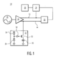
- FIG. 1 is a system block diagram of an exemplary embodiment in accordance with the present invention
- FIG. 2 is a pixel array in accordance with an exemplary embodiment of the present invention.
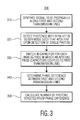
- FIG. 3 is a flow diagram of an exemplary embodiment in accordance with the present invention.
- FIG. 4 is another flow diagram of an exemplary embodiment in accordance with the present invention.
- an analog SiPM using phase detection Measuring the SiPMs timing and energy resolution from the analog current domain to the analog frequency domain provides additional analog processing that may be utilized to screen out GM-APDs that are always turned off or turned on.
- the number of defective GM-APDs may be detected before any digital post-processing is performed, which offers a speed advantage not found in devices that depend on digital post-processing.
- FIG. 1 is a system block diagram of an exemplary embodiment in accordance with the present invention.
- an analog SiPM system 10 includes an analog pixel 12, a first transmission line 14, a second transmission line 16, a signal generator 18, a differential broadband amplifier 20, a phase detector 22, a compensation network 24 and a timer 26.
- the analog pixel 12 includes at least one APD 28, a capacitor 30, a switch 32, an inverter 34, and a quenching resistor 36.
- the analog pixel 12 is coupled to the first transmission line 14 through the switch 32.
- multiple APDs 28 are coupled to the first transmission line 14, in an array format (e.g., arranged in a grid format).
- FIG. 2 illustrates this concept.
- the first transmission line 14 and the second transmission line 16 are configured such that a signal propagated simultaneously on the first transmission line 14 and the second transmission line 16 by the signal generator 18 reach the phase detector 22 at the same time and in the same phase.
- the signal is a sinusoidal signal. Accordingly, if a delay is introduced into either the first transmission line 14 or the second transmission line 16, the phase detector 22 is configured to measure such a phase difference resulting from the delay.
- the signal generator 18 is configured to generate a sinusoidal signal to be propagated approximately simultaneously on the transmission line 14 and the second transmission line 16.
- the differential broadband amplifier 20 is configured to propagate a sinusoidal signal approximately simultaneously on the transmission line 14 and the second transmission line 16.
- the phase detector 22 detects the phase difference between the signal propagated along the first transmission line 14 and the second transmission line 16.
- the phase detector 22 is coupled to the compensation network 24 and provides the compensation network 24 with a signal (e.g., a linear voltage) corresponding to the detected phase difference.
- the compensation network 24 is thereby configured to switch in a number of compensation capacitors (internal to the compensation network 24) corresponding to the number of analog pixels in which an APD 28 has fired. If at least one APD 28 has fired in the analog pixel 12, the capacitor 30 is switched onto the first transmission line 14, causing the sinusoidal signal propagated along the first transmission line 14 to be delayed due to the additional capacitance. This will cause a phase mismatch between the signals transmitted along transmission lines 14 and 16.
- the phase detector 22 will measure this phase difference and signal the compensation network 24 to switch in the requisite number of compensation capacitors to delay the sinusoidal signal propagated along the second transmission line 16.
- the net effect of the delay to the sinusoidal signal propagated along the second transmission line 16 is to equalize the phase difference detected by the phase detector 22, or in other words, to compensate for the delay introduced to the sinusoidal signal by the capacitor 30 when switched onto the first transmission line 14.
- the phase difference outputted by the phase detector 22 also serves to provide a number of photons that have been detected.
- the timer 26 is configured to provide an accurate time that the APD 28 fired.
- the accurate time provided by the timer 26 is useful in determining where any given photon originated from in a Time-of-Flight (TOF) PET system for example.
- TOF Time-of-Flight
- PET systems image the body using two coincident 511 keV gamma photons that are detected by means of scintillation crystals.
- the scintillator crystals stop the gamma photon and convert part of its energy into several optical photons with energies in the blue part of the spectrum. This phenomenon is referred to as a gamma photon hit.
- the optical photons may subsequently be detected by one or more SiPM's in the PET system.
- nanosecond timing resolution is sufficient for the system to detect coincident hits, i.e. hits that are associated with the same positron decay event.
- the timing resolution is improved to below a nanosecond (e.g., the timer 26 is configured to record sub-nanosecond time)
- localization of the particular positron decay event along the line of response defined by the two gamma hits and the additional timing resolution may be utilized to improve the overall quality of the PET image by reducing the signal to noise ratio.
- FIG. 2 is a pixel array in accordance with an exemplary embodiment of the present invention.
- a pixel array 38 includes a number of the analog pixels 12 arranged in an array format, the first transmission line 14, the second transmission line 16 and the phase detector 22.
- the first transmission line 14 and the second transmission line 16 are coupled to each of the analog pixels 12, allowing the detector to measure the phase difference for multiple analog pixels 12.
- the phase difference may also be converted into a voltage and provided as feedback to control the status of each of the analog pixels 12.
- FIG. 3 is a flow diagram of an exemplary embodiment in accordance with the present invention.
- a signal to be propagated along a first transmission line and a second transmission line is generated.
- the signal for example, is a sinusoidal signal.
- photon(s) are detected by utilizing APDs set in Geiger-mode (e.g., GM-APDs).
- the APDs set in Geiger-mode are configured such that the APDs fire-upon detection of a single photon.
- APDs set in Geiger-mode are intrinsically fast due to a very small width of depletion layer and an extremely short time of Geiger-type discharge development (less than 500 ps, in some cases).
- a capacitor is loaded on the first transmission line for each analog pixel in which an APD has fired.
- Each capacitor that is loaded on the first transmission line introduces a delay in the sinusoidal signal propagated along the first transmission line.
- a phase difference between the first transmission line and the second transmission line is determined.
- the phase difference will vary depending on how many capacitors have been loaded on the first transmission line.
- a number of photons detected is calculated from the phase difference. For each capacitor loaded on the first transmission line, the phase difference will increment, therefore enabling a simple algorithm to identify and calculate the number of photons detected.
- the analog SiPM detector system provides a simplified numerical indicator for the number of photons detected for time-of-flight positron emission tomography (PET) systems. Rather than limiting the acquisition and readout phase to post-process implementation in the digital domain, the system may continually allocate and read out information such as the number of photons detected while in operation. This is because the phase difference due to the APD firing will be rapidly accounted for by the compensation network 24, in turn enabling the analog SiPM detector system to immediately become operational once the phase delay has been compensated for. This has the added benefit of virtually hiding the dead time experienced in some systems implementations, due to the 10-15 ns recovery time of a APD, and providing virtually continuous operation of the analog SiPM detector system.
- PTT time-of-flight positron emission tomography
- FIG. 4 is another flow diagram of an exemplary embodiment in accordance with the present invention.
- Blocks 410 through 440 are the same or similar as Blocks 310 through 340 of FIG. 3 .
- Block 430 is written from the perspective of one analog pixel of a pixel array. However, one of ordinary skill in the art would recognize that FIG. 4 may be extrapolated to include multiple analog pixels.
- a number of compensation capacitors are loaded on the second transmission line to equalize the phase difference determined in Block 440. Equalizing the phase difference provides a simplified method to minimize dark time (e.g., recovery time of each analog pixel) since the junction capacitance is more quickly discharged to a steady (e.g., equalized) level.
- phase difference also indicates the number of APDs that are erroneously turned off or turned on, essentially providing a periodic snapshot of the number of working APDs.
- the phase difference is proportional to the number of APDs 12 that have fired.
- the phase detector 22 will measure the phase mismatch and cause the compensation network 24 to switch "n” compensation capacitors onto the transmission line 16 to eliminate the phase mismatch seen by the phase detector 22. Accordingly, a baseline case of "n” capacitors have been switched in. Subsequently, if a number of photons hit the analog photomultiplier 38, "m" APDs 12 will fire and switch their associated capacitors 20 onto the transmission line 14. The phase detector 22 will once more detect a phase mismatch between transmission line 14 and transmission line 16. Consequently, the compensation network will switch “m” more capacitors onto the transmission line 16 to bring the phases back into alignment. The compensation network will now identify "n+m” compensation capacitors on transmission line 16.
- the baseline case, "n" may be subtracted from the “n+m” case to get “m”, the number of APDs 12 that have fired. Over time (10-15ns), the APDs 12 will restore, stop firing, and remove their capacitors 20 from transmission line 14. The phase detector 20 will detect this as a phase mismatch and cause the compensation network to restore the number of switched capacitors back to "n" to bring the phase back into alignment.
- an analog SiPM using phase detection Measuring the SiPM's timing and energy resolution from the analog current domain to the analog frequency domain provides additional analog processing that may be utilized to screen out GM-APDs that are always turned off or turned on.
- the number of defective GM-APDs may be detected before any digital post-processing is performed, which offers a speed advantage not found in devices that depend on digital post-processing.
Landscapes
- Physics & Mathematics (AREA)
- Health & Medical Sciences (AREA)
- Life Sciences & Earth Sciences (AREA)
- General Physics & Mathematics (AREA)
- High Energy & Nuclear Physics (AREA)
- Molecular Biology (AREA)
- Spectroscopy & Molecular Physics (AREA)
- Engineering & Computer Science (AREA)
- Biomedical Technology (AREA)
- General Health & Medical Sciences (AREA)
- Medical Informatics (AREA)
- Nuclear Medicine, Radiotherapy & Molecular Imaging (AREA)
- Optics & Photonics (AREA)
- Light Receiving Elements (AREA)
- Photometry And Measurement Of Optical Pulse Characteristics (AREA)
Claims (14)
- Ein analoges Silizium Photomultipliersystem, das konfiguriert ist, um Nieder-Energie Photonenemissionen zu detektieren, das System aufweisend:zumindest ein analoges Pixel (12), das eine Mehrzahl von Lawinenphotodioden, auch APDs (28) genannt, und einen Kondensator (30) aufweist, wobei die APDs konfiguriert sind, um bei einer Detektion eines Photons abzufeuern,einen Signalgenerator (18), der konfiguriert ist, um ein sinusförmiges Signal gleichzeitig entlang einer ersten Übertragungsleitung (14) und einer zweiten Übertragungsleitung (16) zu generieren und zu übertragen, wobei der Kondensator konfiguriert ist, um auf der ersten Übertragungsleitung aufgeladen zu werden, wenn eine APD der Mehrzahl von APDs in dem zumindest einen analogen Pixel, das zu dem Kondensator korrespondiert, ein Photon detektiert,einen Phasendetektor (22), der mit der ersten Übertragungsleitung (14) und der zweiten Übertragungsleitung (16) gekoppelt ist, wobei der Phasendetektor konfiguriert ist, um eine Phasendifferenz zwischen der ersten Übertragungsleitung und der zweiten Übertragungsleitung zu bestimmen und eine Anzahl von APDs zu berechnen, die aus der Phasendifferenz abgefeuert haben, undein Kompensationsnetzwerk (24), das mit der zweiten Übertragungsleitung (16) und dem Phasendetektor (22) gekoppelt ist, wobei das Kompensationsnetzwerk eine Mehrzahl von Kompensationskondensatoren aufweist, wobei die Kompensationskondensatoren konfiguriert sind, um auf der zweiten Übertragungsleitung in Proportion zu der Anzahl von APDs, die abgefeuert haben, aufgeladen zu werden.
- Das analoges Silizium Photomultipliersystem gemäß Anspruch 1, wobei das Kompensationsnetzwerk die Anzahl von APDs, die abgefeuert haben, bestimmt.
- Das analoges Silizium Photomultipliersystem gemäß Anspruch 1, das System ferner aufweisend:einen an den Phasendetektor gekoppelten Timer, der konfiguriert ist, um eine Zeit für jedes Mal, wenn die Anzahl von APDs abgefeuert hat, zu speichern.
- Das analoges Silizium Photomultipliersystem gemäß Anspruch 3, wobei der Timer konfiguriert ist, um eine Sub-Nanosekunden Zeit zu speichern.
- Das analoges Silizium Photomultipliersystem gemäß Anspruch 1, wobei die Mehrzahl von APDs konfiguriert sind, um in einem Geigermodus betrieben zu werden.
- Das analoges Silizium Photomultipliersystem gemäß Anspruch 1, wobei der Phasendetektor eine Spannung an das Kompensationsnetzwerk ausgibt, die zu der Phasendifferenz korrespondiert.
- Das analoges Silizium Photomultipliersystem gemäß Anspruch 1, wobei die Mehrzahl von APDs ferner ein Array von APDs aufweist, die in einem Gitter angeordnet sind.
- Ein Verfahren zum Bestimmen einer Anzahl von Photonen, die in einem Pixelarray detektiert werden, wobei das Pixelarray eine Mehrzahl von analogen Pixeln beinhaltet, wobei jedes der analogen Pixel eine Mehrzahl von Lawinenphotodioden (APDs) und einen Kondensator aufweist, das Verfahren aufweisend:Generieren eines zu übertragenden Signals gleichzeitig entlang einer ersten Übertragungsleitung und einer zweiten Übertragungsleitung, wobei die Mehrzahl der analogen Pixel an die erste Übertragungsleitung gekoppelt ist,Detektieren zumindest eines Photons mit dem Pixelarray, wobei jede der APDs konfiguriert ist, um bei einem Detektieren des zumindest einen Photons abzufeuern,Anschalten eines Schalters, wenn zumindest eine der APDs für jedes der analogen Pixel abgefeuert hat, wobei der Kondensator auf der ersten Übertragungsleitung aufgeladen wird, wenn der Schalter angeschaltet ist, undBestimmen einer Phasendifferenz zwischen der ersten Übertragungsleitung und der zweiten Übertragungsleitung, wobei die Phasendifferenz die Anzahl der Photonen anzeigt, die mittels des Pixelarrays detektiert werden.
- Das Verfahren gemäß Anspruch 8, aufweisend:Speichern einer Zeit, bei der jede APD der Mehrzahl von APDs abgefeuert hat.
- Das Verfahren gemäß Anspruch 9, wobei die Zeit, bei der jede APD der Mehrzahl von APDs abgefeuert hat, auf eine Sub-Nanosekunden Zeit gespeichert wird.
- Das Verfahren gemäß Anspruch 8, wobei die Mehrzahl von APDs konfiguriert ist, um in einem Geigermodus betrieben zu werden.
- Das Verfahren gemäß Anspruch 8, wobei die Phasendifferenz in eine lineare Spannung konvertiert wird, um die Anzahl der Photonen anzuzeigen, die mittels des Pixelarrays detektiert werden.
- Ein Verfahren zum Kompensieren für nicht-reagierende Lawinenphotodioden (APDs) in einem analogen Pixel eines Pixelarrays, wobei das analoge Pixel eine Mehrzahl von APDs und einen Kondensator aufweist, das Verfahren aufweisend:Generieren eines zu übertragenden Signals gleichzeitig entlang einer ersten Übertragungsleitung und einer zweiten Übertragungsleitung, wobei das analoge Pixel an die erste Übertragungsleitung gekoppelt ist,Detektieren zumindest eines Photons mit dem analogen Pixel, wobei jede der APDs des analogen Pixels konfiguriert ist, um bei einem Detektieren des zumindest einen Photons abzufeuern,Anschalten eines Schalters, wenn zumindest eine der APDs abgefeuert hat, wobei der Kondensator auf der ersten Übertragungsleitung aufgeladen wird, wenn der Schalter angeschaltet ist,Bestimmen einer Phasendifferenz zwischen der ersten Übertragungsleitung und der zweiten Übertragungsleitung, undAufladen zumindest eines Kompensationskondensators auf der zweiten Übertragungsleitung, um die Phasendifferenz zwischen der ersten Übertragungsleitung und der zweiten Übertragungsleitung auszugleichen.
- Das Verfahren gemäß Anspruch 12, wobei die Mehrzahl von APDs konfiguriert ist, um in einem Geigermodus betrieben zu werden.
Applications Claiming Priority (2)
| Application Number | Priority Date | Filing Date | Title |
|---|---|---|---|
| US19866808P | 2008-11-07 | 2008-11-07 | |
| PCT/IB2009/054949 WO2010052674A2 (en) | 2008-11-07 | 2009-11-06 | Analog silicon photomultiplier using phase detection |
Publications (2)
| Publication Number | Publication Date |
|---|---|
| EP2353032A2 EP2353032A2 (de) | 2011-08-10 |
| EP2353032B1 true EP2353032B1 (de) | 2012-08-15 |
Family
ID=42153352
Family Applications (1)
| Application Number | Title | Priority Date | Filing Date |
|---|---|---|---|
| EP09756184A Active EP2353032B1 (de) | 2008-11-07 | 2009-11-06 | Analoger silizium-photovervielfacher mit phasendetektion |
Country Status (3)
| Country | Link |
|---|---|
| US (1) | US8716647B2 (de) |
| EP (1) | EP2353032B1 (de) |
| WO (1) | WO2010052674A2 (de) |
Families Citing this family (8)
| Publication number | Priority date | Publication date | Assignee | Title |
|---|---|---|---|---|
| US8766161B2 (en) * | 2009-12-02 | 2014-07-01 | Nucript LLC | System for controling and calibrating single photon detection devices |
| GB201004922D0 (en) * | 2010-03-24 | 2010-05-12 | Sensl Technologies Ltd | Silicon photomultiplier and readout method |
| US9606245B1 (en) | 2015-03-24 | 2017-03-28 | The Research Foundation For The State University Of New York | Autonomous gamma, X-ray, and particle detector |
| US10371835B2 (en) | 2016-01-11 | 2019-08-06 | General Electric Company | Microcell interconnection in silicon photomultipliers |
| US9939536B2 (en) | 2016-02-19 | 2018-04-10 | Sensi Technologies Ltd. | Semiconductor photomultiplier with baseline restoration for a fast terminal signal output including output loads to correct an overshoot of an output signal (as amended) |
| US10673204B2 (en) | 2017-03-07 | 2020-06-02 | Sensl Technologies Ltd. | Laser driver |
| JP6924085B2 (ja) * | 2017-06-27 | 2021-08-25 | キヤノン株式会社 | 光検出装置及び撮像システム |
| US10635168B2 (en) * | 2017-08-22 | 2020-04-28 | Microsoft Technology Licensing, Llc | MEMS line scanner and silicon photomultiplier based pixel camera for low light large dynamic range eye imaging |
Family Cites Families (6)
| Publication number | Priority date | Publication date | Assignee | Title |
|---|---|---|---|---|
| JP3441169B2 (ja) * | 1994-07-06 | 2003-08-25 | 浜松ホトニクス株式会社 | 同期型信号検出装置 |
| WO2006111883A2 (en) | 2005-04-22 | 2006-10-26 | Koninklijke Philips Electronics, N.V. | Digital silicon photomultiplier for tof-pet |
| JP5326081B2 (ja) * | 2006-03-06 | 2013-10-30 | 学校法人日本大学 | 光通信波長帯高速単一光子検出器 |
| WO2010029638A1 (ja) * | 2008-09-12 | 2010-03-18 | 三菱電機株式会社 | 光子検出器 |
| GB2475235B (en) * | 2009-11-09 | 2014-01-08 | Toshiba Res Europ Ltd | A photon detector |
| GB2483518B8 (en) * | 2010-09-13 | 2015-07-22 | Toshiba Res Europ Ltd | A receiver for a quantum communication system |
-
2009
- 2009-11-06 US US13/127,786 patent/US8716647B2/en active Active
- 2009-11-06 WO PCT/IB2009/054949 patent/WO2010052674A2/en not_active Ceased
- 2009-11-06 EP EP09756184A patent/EP2353032B1/de active Active
Also Published As
| Publication number | Publication date |
|---|---|
| EP2353032A2 (de) | 2011-08-10 |
| US8716647B2 (en) | 2014-05-06 |
| WO2010052674A3 (en) | 2010-10-07 |
| US20110315856A1 (en) | 2011-12-29 |
| WO2010052674A2 (en) | 2010-05-14 |
Similar Documents
| Publication | Publication Date | Title |
|---|---|---|
| US8716647B2 (en) | Analog silicon photomultiplier using phase detection | |
| JP6209683B2 (ja) | 光子を検出する検出デバイス及びそのための方法 | |
| RU2411542C2 (ru) | Цифровой кремниевый фотоумножитель для врп-пэт | |
| JP5644294B2 (ja) | 光検出器 | |
| EP2257835B1 (de) | Einzelphotonen-strahlungsdetektor | |
| CN101861527B (zh) | 硅光电倍增器触发网络 | |
| US9354332B2 (en) | Detector array with time-to-digital conversion having improved temporal accuracy | |
| JP5901523B2 (ja) | 単一光子分解能のための積算形読み出しチップを有するx線検出器 | |
| US10527740B2 (en) | Silicon photomultiplier based TOF-PET detector | |
| Gola et al. | The DLED algorithm for timing measurements on large area SiPMs coupled to scintillators | |
| CA2690387A1 (en) | Digitizer for a digital imaging system | |
| US20190302240A1 (en) | Dual mode stacked photomultipliers suitable for use in long range time of flight applications | |
| WO2017016469A1 (zh) | 光子测量前端电路 | |
| US11047996B2 (en) | Photodetector | |
| US10838088B2 (en) | Apparatus, device and method for measuring gain of sensor | |
| JP2014228464A (ja) | 放射線計測装置および放射線計測方法 | |
| WO2020018602A1 (en) | High-sensitivity depth sensor with non-avalanche photodetector | |
| Auger et al. | Multi-channel front-end board for SiPM readout | |
| JP7057630B2 (ja) | 放射線検出装置 | |
| Dolinsky et al. | Timing resolution performance comparison of different SiPM devices | |
| Meyer et al. | A time-based front end readout system for PET & CT | |
| Doroud et al. | The Strip Silicon Photo-Multiplier: An innovation for enhanced time and position measurement | |
| WO2024124367A1 (en) | Neutron detector | |
| US10175367B2 (en) | Tool for detecting photon radiation, particularly adapted for high-flux radiation | |
| JP2025104954A (ja) | 光検出器および光検出装置 |
Legal Events
| Date | Code | Title | Description |
|---|---|---|---|
| PUAI | Public reference made under article 153(3) epc to a published international application that has entered the european phase |
Free format text: ORIGINAL CODE: 0009012 |
|
| 17P | Request for examination filed |
Effective date: 20110607 |
|
| AK | Designated contracting states |
Kind code of ref document: A2 Designated state(s): AT BE BG CH CY CZ DE DK EE ES FI FR GB GR HR HU IE IS IT LI LT LU LV MC MK MT NL NO PL PT RO SE SI SK SM TR |
|
| REG | Reference to a national code |
Ref country code: DE Ref legal event code: R079 Ref document number: 602009009030 Country of ref document: DE Free format text: PREVIOUS MAIN CLASS: G01T0001208000 Ipc: G01T0001164000 |
|
| RIC1 | Information provided on ipc code assigned before grant |
Ipc: G01T 1/164 20060101AFI20111013BHEP Ipc: G01T 1/24 20060101ALI20111013BHEP |
|
| DAX | Request for extension of the european patent (deleted) | ||
| GRAP | Despatch of communication of intention to grant a patent |
Free format text: ORIGINAL CODE: EPIDOSNIGR1 |
|
| GRAS | Grant fee paid |
Free format text: ORIGINAL CODE: EPIDOSNIGR3 |
|
| GRAA | (expected) grant |
Free format text: ORIGINAL CODE: 0009210 |
|
| AK | Designated contracting states |
Kind code of ref document: B1 Designated state(s): AT BE BG CH CY CZ DE DK EE ES FI FR GB GR HR HU IE IS IT LI LT LU LV MC MK MT NL NO PL PT RO SE SI SK SM TR |
|
| REG | Reference to a national code |
Ref country code: CH Ref legal event code: EP Ref country code: AT Ref legal event code: REF Ref document number: 571115 Country of ref document: AT Kind code of ref document: T Effective date: 20120815 Ref country code: GB Ref legal event code: FG4D |
|
| REG | Reference to a national code |
Ref country code: IE Ref legal event code: FG4D |
|
| REG | Reference to a national code |
Ref country code: DE Ref legal event code: R096 Ref document number: 602009009030 Country of ref document: DE Effective date: 20121011 |
|
| REG | Reference to a national code |
Ref country code: NL Ref legal event code: VDEP Effective date: 20120815 |
|
| REG | Reference to a national code |
Ref country code: AT Ref legal event code: MK05 Ref document number: 571115 Country of ref document: AT Kind code of ref document: T Effective date: 20120815 |
|
| PG25 | Lapsed in a contracting state [announced via postgrant information from national office to epo] |
Ref country code: IS Free format text: LAPSE BECAUSE OF FAILURE TO SUBMIT A TRANSLATION OF THE DESCRIPTION OR TO PAY THE FEE WITHIN THE PRESCRIBED TIME-LIMIT Effective date: 20121215 Ref country code: NO Free format text: LAPSE BECAUSE OF FAILURE TO SUBMIT A TRANSLATION OF THE DESCRIPTION OR TO PAY THE FEE WITHIN THE PRESCRIBED TIME-LIMIT Effective date: 20121115 Ref country code: LT Free format text: LAPSE BECAUSE OF FAILURE TO SUBMIT A TRANSLATION OF THE DESCRIPTION OR TO PAY THE FEE WITHIN THE PRESCRIBED TIME-LIMIT Effective date: 20120815 Ref country code: FI Free format text: LAPSE BECAUSE OF FAILURE TO SUBMIT A TRANSLATION OF THE DESCRIPTION OR TO PAY THE FEE WITHIN THE PRESCRIBED TIME-LIMIT Effective date: 20120815 Ref country code: AT Free format text: LAPSE BECAUSE OF FAILURE TO SUBMIT A TRANSLATION OF THE DESCRIPTION OR TO PAY THE FEE WITHIN THE PRESCRIBED TIME-LIMIT Effective date: 20120815 Ref country code: HR Free format text: LAPSE BECAUSE OF FAILURE TO SUBMIT A TRANSLATION OF THE DESCRIPTION OR TO PAY THE FEE WITHIN THE PRESCRIBED TIME-LIMIT Effective date: 20120815 |
|
| PG25 | Lapsed in a contracting state [announced via postgrant information from national office to epo] |
Ref country code: BE Free format text: LAPSE BECAUSE OF FAILURE TO SUBMIT A TRANSLATION OF THE DESCRIPTION OR TO PAY THE FEE WITHIN THE PRESCRIBED TIME-LIMIT Effective date: 20120815 Ref country code: LV Free format text: LAPSE BECAUSE OF FAILURE TO SUBMIT A TRANSLATION OF THE DESCRIPTION OR TO PAY THE FEE WITHIN THE PRESCRIBED TIME-LIMIT Effective date: 20120815 Ref country code: GR Free format text: LAPSE BECAUSE OF FAILURE TO SUBMIT A TRANSLATION OF THE DESCRIPTION OR TO PAY THE FEE WITHIN THE PRESCRIBED TIME-LIMIT Effective date: 20121116 Ref country code: PL Free format text: LAPSE BECAUSE OF FAILURE TO SUBMIT A TRANSLATION OF THE DESCRIPTION OR TO PAY THE FEE WITHIN THE PRESCRIBED TIME-LIMIT Effective date: 20120815 Ref country code: PT Free format text: LAPSE BECAUSE OF FAILURE TO SUBMIT A TRANSLATION OF THE DESCRIPTION OR TO PAY THE FEE WITHIN THE PRESCRIBED TIME-LIMIT Effective date: 20121217 Ref country code: SI Free format text: LAPSE BECAUSE OF FAILURE TO SUBMIT A TRANSLATION OF THE DESCRIPTION OR TO PAY THE FEE WITHIN THE PRESCRIBED TIME-LIMIT Effective date: 20120815 Ref country code: SE Free format text: LAPSE BECAUSE OF FAILURE TO SUBMIT A TRANSLATION OF THE DESCRIPTION OR TO PAY THE FEE WITHIN THE PRESCRIBED TIME-LIMIT Effective date: 20120815 |
|
| PG25 | Lapsed in a contracting state [announced via postgrant information from national office to epo] |
Ref country code: NL Free format text: LAPSE BECAUSE OF FAILURE TO SUBMIT A TRANSLATION OF THE DESCRIPTION OR TO PAY THE FEE WITHIN THE PRESCRIBED TIME-LIMIT Effective date: 20120815 |
|
| PG25 | Lapsed in a contracting state [announced via postgrant information from national office to epo] |
Ref country code: RO Free format text: LAPSE BECAUSE OF FAILURE TO SUBMIT A TRANSLATION OF THE DESCRIPTION OR TO PAY THE FEE WITHIN THE PRESCRIBED TIME-LIMIT Effective date: 20120815 Ref country code: CZ Free format text: LAPSE BECAUSE OF FAILURE TO SUBMIT A TRANSLATION OF THE DESCRIPTION OR TO PAY THE FEE WITHIN THE PRESCRIBED TIME-LIMIT Effective date: 20120815 Ref country code: DK Free format text: LAPSE BECAUSE OF FAILURE TO SUBMIT A TRANSLATION OF THE DESCRIPTION OR TO PAY THE FEE WITHIN THE PRESCRIBED TIME-LIMIT Effective date: 20120815 Ref country code: EE Free format text: LAPSE BECAUSE OF FAILURE TO SUBMIT A TRANSLATION OF THE DESCRIPTION OR TO PAY THE FEE WITHIN THE PRESCRIBED TIME-LIMIT Effective date: 20120815 |
|
| PG25 | Lapsed in a contracting state [announced via postgrant information from national office to epo] |
Ref country code: IT Free format text: LAPSE BECAUSE OF FAILURE TO SUBMIT A TRANSLATION OF THE DESCRIPTION OR TO PAY THE FEE WITHIN THE PRESCRIBED TIME-LIMIT Effective date: 20120815 Ref country code: SK Free format text: LAPSE BECAUSE OF FAILURE TO SUBMIT A TRANSLATION OF THE DESCRIPTION OR TO PAY THE FEE WITHIN THE PRESCRIBED TIME-LIMIT Effective date: 20120815 |
|
| PLBE | No opposition filed within time limit |
Free format text: ORIGINAL CODE: 0009261 |
|
| STAA | Information on the status of an ep patent application or granted ep patent |
Free format text: STATUS: NO OPPOSITION FILED WITHIN TIME LIMIT |
|
| 26N | No opposition filed |
Effective date: 20130516 |
|
| PG25 | Lapsed in a contracting state [announced via postgrant information from national office to epo] |
Ref country code: BG Free format text: LAPSE BECAUSE OF FAILURE TO SUBMIT A TRANSLATION OF THE DESCRIPTION OR TO PAY THE FEE WITHIN THE PRESCRIBED TIME-LIMIT Effective date: 20121115 |
|
| REG | Reference to a national code |
Ref country code: IE Ref legal event code: MM4A |
|
| REG | Reference to a national code |
Ref country code: DE Ref legal event code: R097 Ref document number: 602009009030 Country of ref document: DE Effective date: 20130516 |
|
| PG25 | Lapsed in a contracting state [announced via postgrant information from national office to epo] |
Ref country code: IE Free format text: LAPSE BECAUSE OF NON-PAYMENT OF DUE FEES Effective date: 20121106 Ref country code: ES Free format text: LAPSE BECAUSE OF FAILURE TO SUBMIT A TRANSLATION OF THE DESCRIPTION OR TO PAY THE FEE WITHIN THE PRESCRIBED TIME-LIMIT Effective date: 20121126 |
|
| PG25 | Lapsed in a contracting state [announced via postgrant information from national office to epo] |
Ref country code: CY Free format text: LAPSE BECAUSE OF FAILURE TO SUBMIT A TRANSLATION OF THE DESCRIPTION OR TO PAY THE FEE WITHIN THE PRESCRIBED TIME-LIMIT Effective date: 20120815 Ref country code: MT Free format text: LAPSE BECAUSE OF FAILURE TO SUBMIT A TRANSLATION OF THE DESCRIPTION OR TO PAY THE FEE WITHIN THE PRESCRIBED TIME-LIMIT Effective date: 20120815 |
|
| PG25 | Lapsed in a contracting state [announced via postgrant information from national office to epo] |
Ref country code: MC Free format text: LAPSE BECAUSE OF NON-PAYMENT OF DUE FEES Effective date: 20121130 Ref country code: TR Free format text: LAPSE BECAUSE OF FAILURE TO SUBMIT A TRANSLATION OF THE DESCRIPTION OR TO PAY THE FEE WITHIN THE PRESCRIBED TIME-LIMIT Effective date: 20120815 |
|
| PG25 | Lapsed in a contracting state [announced via postgrant information from national office to epo] |
Ref country code: LU Free format text: LAPSE BECAUSE OF NON-PAYMENT OF DUE FEES Effective date: 20121106 Ref country code: SM Free format text: LAPSE BECAUSE OF FAILURE TO SUBMIT A TRANSLATION OF THE DESCRIPTION OR TO PAY THE FEE WITHIN THE PRESCRIBED TIME-LIMIT Effective date: 20120815 |
|
| REG | Reference to a national code |
Ref country code: CH Ref legal event code: PL |
|
| PG25 | Lapsed in a contracting state [announced via postgrant information from national office to epo] |
Ref country code: CH Free format text: LAPSE BECAUSE OF NON-PAYMENT OF DUE FEES Effective date: 20131130 Ref country code: HU Free format text: LAPSE BECAUSE OF FAILURE TO SUBMIT A TRANSLATION OF THE DESCRIPTION OR TO PAY THE FEE WITHIN THE PRESCRIBED TIME-LIMIT Effective date: 20091106 Ref country code: LI Free format text: LAPSE BECAUSE OF NON-PAYMENT OF DUE FEES Effective date: 20131130 |
|
| PG25 | Lapsed in a contracting state [announced via postgrant information from national office to epo] |
Ref country code: MK Free format text: LAPSE BECAUSE OF FAILURE TO SUBMIT A TRANSLATION OF THE DESCRIPTION OR TO PAY THE FEE WITHIN THE PRESCRIBED TIME-LIMIT Effective date: 20120815 |
|
| REG | Reference to a national code |
Ref country code: FR Ref legal event code: PLFP Year of fee payment: 7 |
|
| REG | Reference to a national code |
Ref country code: FR Ref legal event code: PLFP Year of fee payment: 8 |
|
| REG | Reference to a national code |
Ref country code: FR Ref legal event code: PLFP Year of fee payment: 9 |
|
| REG | Reference to a national code |
Ref country code: FR Ref legal event code: PLFP Year of fee payment: 10 |
|
| P01 | Opt-out of the competence of the unified patent court (upc) registered |
Effective date: 20230724 |
|
| PGFP | Annual fee paid to national office [announced via postgrant information from national office to epo] |
Ref country code: DE Payment date: 20251022 Year of fee payment: 17 |
|
| PGFP | Annual fee paid to national office [announced via postgrant information from national office to epo] |
Ref country code: GB Payment date: 20251022 Year of fee payment: 17 |
|
| PGFP | Annual fee paid to national office [announced via postgrant information from national office to epo] |
Ref country code: FR Payment date: 20251022 Year of fee payment: 17 |