EP2357681A2 - Dispositif électroluminescent et unité d'éclairage - Google Patents
Dispositif électroluminescent et unité d'éclairage Download PDFInfo
- Publication number
- EP2357681A2 EP2357681A2 EP11154427A EP11154427A EP2357681A2 EP 2357681 A2 EP2357681 A2 EP 2357681A2 EP 11154427 A EP11154427 A EP 11154427A EP 11154427 A EP11154427 A EP 11154427A EP 2357681 A2 EP2357681 A2 EP 2357681A2
- Authority
- EP
- European Patent Office
- Prior art keywords
- light emitting
- emitting device
- layer
- type semiconductor
- semiconductor layer
- Prior art date
- Legal status (The legal status is an assumption and is not a legal conclusion. Google has not performed a legal analysis and makes no representation as to the accuracy of the status listed.)
- Granted
Links
Images




Classifications
-
- H—ELECTRICITY
- H10—SEMICONDUCTOR DEVICES; ELECTRIC SOLID-STATE DEVICES NOT OTHERWISE PROVIDED FOR
- H10H—INORGANIC LIGHT-EMITTING SEMICONDUCTOR DEVICES HAVING POTENTIAL BARRIERS
- H10H20/00—Individual inorganic light-emitting semiconductor devices having potential barriers, e.g. light-emitting diodes [LED]
- H10H20/80—Constructional details
- H10H20/81—Bodies
- H10H20/819—Bodies characterised by their shape, e.g. curved or truncated substrates
-
- H—ELECTRICITY
- H10—SEMICONDUCTOR DEVICES; ELECTRIC SOLID-STATE DEVICES NOT OTHERWISE PROVIDED FOR
- H10H—INORGANIC LIGHT-EMITTING SEMICONDUCTOR DEVICES HAVING POTENTIAL BARRIERS
- H10H20/00—Individual inorganic light-emitting semiconductor devices having potential barriers, e.g. light-emitting diodes [LED]
- H10H20/80—Constructional details
- H10H20/83—Electrodes
- H10H20/831—Electrodes characterised by their shape
-
- H—ELECTRICITY
- H10—SEMICONDUCTOR DEVICES; ELECTRIC SOLID-STATE DEVICES NOT OTHERWISE PROVIDED FOR
- H10W—GENERIC PACKAGES, INTERCONNECTIONS, CONNECTORS OR OTHER CONSTRUCTIONAL DETAILS OF DEVICES COVERED BY CLASS H10
- H10W72/00—Interconnections or connectors in packages
- H10W72/30—Die-attach connectors
-
- H—ELECTRICITY
- H10—SEMICONDUCTOR DEVICES; ELECTRIC SOLID-STATE DEVICES NOT OTHERWISE PROVIDED FOR
- H10W—GENERIC PACKAGES, INTERCONNECTIONS, CONNECTORS OR OTHER CONSTRUCTIONAL DETAILS OF DEVICES COVERED BY CLASS H10
- H10W72/00—Interconnections or connectors in packages
- H10W72/90—Bond pads, in general
-
- H—ELECTRICITY
- H10—SEMICONDUCTOR DEVICES; ELECTRIC SOLID-STATE DEVICES NOT OTHERWISE PROVIDED FOR
- H10H—INORGANIC LIGHT-EMITTING SEMICONDUCTOR DEVICES HAVING POTENTIAL BARRIERS
- H10H20/00—Individual inorganic light-emitting semiconductor devices having potential barriers, e.g. light-emitting diodes [LED]
- H10H20/80—Constructional details
- H10H20/85—Packages
- H10H20/857—Interconnections, e.g. lead-frames, bond wires or solder balls
-
- H—ELECTRICITY
- H10—SEMICONDUCTOR DEVICES; ELECTRIC SOLID-STATE DEVICES NOT OTHERWISE PROVIDED FOR
- H10W—GENERIC PACKAGES, INTERCONNECTIONS, CONNECTORS OR OTHER CONSTRUCTIONAL DETAILS OF DEVICES COVERED BY CLASS H10
- H10W72/00—Interconnections or connectors in packages
- H10W72/071—Connecting or disconnecting
- H10W72/073—Connecting or disconnecting of die-attach connectors
- H10W72/07321—Aligning
- H10W72/07327—Aligning involving guiding structures, e.g. spacers or supporting members
-
- H—ELECTRICITY
- H10—SEMICONDUCTOR DEVICES; ELECTRIC SOLID-STATE DEVICES NOT OTHERWISE PROVIDED FOR
- H10W—GENERIC PACKAGES, INTERCONNECTIONS, CONNECTORS OR OTHER CONSTRUCTIONAL DETAILS OF DEVICES COVERED BY CLASS H10
- H10W72/00—Interconnections or connectors in packages
- H10W72/071—Connecting or disconnecting
- H10W72/073—Connecting or disconnecting of die-attach connectors
- H10W72/07331—Connecting techniques
-
- H—ELECTRICITY
- H10—SEMICONDUCTOR DEVICES; ELECTRIC SOLID-STATE DEVICES NOT OTHERWISE PROVIDED FOR
- H10W—GENERIC PACKAGES, INTERCONNECTIONS, CONNECTORS OR OTHER CONSTRUCTIONAL DETAILS OF DEVICES COVERED BY CLASS H10
- H10W72/00—Interconnections or connectors in packages
- H10W72/071—Connecting or disconnecting
- H10W72/073—Connecting or disconnecting of die-attach connectors
- H10W72/07331—Connecting techniques
- H10W72/07336—Soldering or alloying
-
- H—ELECTRICITY
- H10—SEMICONDUCTOR DEVICES; ELECTRIC SOLID-STATE DEVICES NOT OTHERWISE PROVIDED FOR
- H10W—GENERIC PACKAGES, INTERCONNECTIONS, CONNECTORS OR OTHER CONSTRUCTIONAL DETAILS OF DEVICES COVERED BY CLASS H10
- H10W72/00—Interconnections or connectors in packages
- H10W72/90—Bond pads, in general
- H10W72/931—Shapes of bond pads
Definitions
- Inventions relate to a light emitting device and a light unit.
- LEDs Light emitting diodes
- LEDs are semiconductor light emitting devices that convert current into light. As luminance of LEDs is increased recently, the LEDs are being used as light sources for displays, vehicles, and illuminations. Also, LEDs emitting highly efficient white light may be realized by using a fluorescent substance or combining LEDs having various colors.
- Inventions provide a light emitting device having a new structure and a light unit.
- Inventions also provide a light emitting device having improved reliability and a light unit.
- a light emitting device includes: a package body including a body, a plurality of electrodes on the body, and a concave portion on at least one of the plurality of electrodes; a light emitting chip including a convex portion at a lower surface thereof corresponding to the concave portion to couple and attach the concave portion to the convex portion, the light emitting chip including a first conductive type semiconductor layer, a second conductive type semiconductor layer, and an active layer between the first conductive type semiconductor layer and the second conductive type semiconductor layer; and an adhesion layer on a lower surface of the light emitting chip.
- a light emitting device in another invention, includes: a package body comprising a body, a plurality of electrodes on the body, and a concave portion on at least one of the plurality of electrodes; a light emitting chip including a convex portion at a lower surface thereof corresponding to the concave portion, wherein the light emitting chip includes a first conductive type semiconductor layer, an active layer, and a second conductive type semiconductor layer; and an adhesion layer on the lower surface of the light emitting chip, wherein the light emitting chip includes a conductive support member under the first conductive type semiconductor layer, the active layer, and the second conductive type semiconductor layer, and wherein the convex portion is formed on a lower surface of the conductive support member.
- Fig. 1 is a view of a light emitting device according to a first invention.
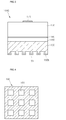
- Figs. 2 and 3 are sectional views of a light emitting chip attached to the light emitting device of Fig. 1 .
- Figs. 4 and 5 are views illustrating various examples of a convex portion disposed on the light emitting chip.
- Fig. 6 is a view of a light emitting device according to a second invention.
- Fig. 7 is a view illustrating a process of attaching a light emitting chip to a package body.
- Fig. 8 is a view of a light emitting device according to a third invention.
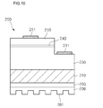
- Figs. 9 and 10 are sectional views of a light emitting chip attached to the light emitting device of Fig. 8 .
- Figs. 11 and 12 are views of a light unit using a light emitting device according to an invention.
- a layer (or film), a region, a pattern, or a structure is referred to as being on' a substrate, a layer (or film), a region, a pad, or patterns, it can be directly on another layer or substrate, or intervening layers may also be present. Further, it will be understood that when a layer is referred to as being 'under' another layer, it can be directly under another layer, and one or more intervening layers may also be present. Further, the reference about 'on' and 'under' each layer will be made on the basis of drawings.
- each layer is exaggerated, omitted, or schematically illustrated for convenience in description and clarity. Also, the size of each element does not entirely reflect an actual size.
- Fig. 1 is a view of a light emitting device according to a first invention.
- a light emitting device includes a body 11, a plurality of electrodes 31 and 32 disposed on the body 11, a package body 10 including a concave portion 35 disposed on at least one of the plurality of electrodes 31 and 32, and a light emitting chip 100 including a convex portion 181 at a lower surface thereof corresponding to the concave portion 35 and attached to the package body 10.
- the body 11 constitutes a body of the package body 10.
- the body 11 may be formed of silicon (Si), aluminum (Al), aluminum nitride (AIN), Alo x , photo sensitive glass (PSG), sapphire (A1 2 O 3 ), beryllium oxide, a printed circuit board (PCB), or various resins, but is not limited thereto.
- the body 11 may be manufactured using injection molding, or a plurality of layers may be stacked to manufacture the body.
- a cavity 15 having an opened upper side may be defined in the body 11.
- the cavity 15 may be formed by injection molding or etching.
- the cavity 15 may have a cup shape and a concave container shape.
- the cavity 15 may have a vertical or inclined inner side surface.
- the cavity 15 may have a surface configuration such as a circular shape, a square shape, a polygonal shape, or an oval shape.
- an insulation layer may be disposed on a surface of the body 11. The insulation layer may prevent the light emitting device from being electrically shorted.
- the plurality of electrodes 31 and 32 may be disposed on the body 11.
- the plurality of electrodes 31 and 32 may include a first electrode 31 and a second electrode 32.
- the first electrode 31 and the second electrode 32 respectively are electrically separated into a positive pole and a negative pole to provide a power to the light emitting chip 100.
- the first and second electrodes 31 and 32 may be formed of a metal containing at least one of Ti, Cu, Ni, and Au. Also, the first and second electrodes 31 and 32 may be selectively manufactured using a plating method, a deposition method, or a photolithograph process, but is not limited thereto.
- the concave portion 35 may be disposed on at least one of the plurality of electrodes 31 and 32.
- the concave portion 35 may be changed in position according to an electrode structure of the light emitting chip 100 and/or a design of the package body 10.
- a mask pattern may be formed using a photolithograph process, and then an etching process may be performed along the mask pattern to form the concave portion 35, but is not limited thereto.
- the concave portion 35 may have a shape corresponding to that of the convex portion 181 disposed on the lower surface of the light emitting chip 100.
- the concave portion 35 may be formed in a plurality and the convex portion 181 may be formed in a plurality.
- the convex portion 181 disposed on the lower surface of the light emitting chip 100 may be attached to the package body 10 by being coupled the concave portion 35.
- the concave portion 35 and the convex portion 181 may be engaged with each other to firmly fix the light emitting chip 100 on the package body 10 without being twisted out of position.
- the light emitting chip 100 is attached to the package body 10 by eutectic bonding or bonding using a bonding paste.
- the light emitting chip 100 may not be accurately attached in a desired position and thus is slightly twisted out of the desired position.
- the concave portion 35 and the convex portion 181 are respectively disposed on the package body 10 and the light emitting chip 100, it may prevent the light emitting chip 100 from being twisted in the eutectic bonding or the bonding using the adhesion layer such as the adhesive formed of the resin material. Therefore, reliability of the light emitting device may be improved.
- Fig. 2 is a sectional view of the light emitting chip 100 according to the first invention
- Fig. 3 is a sectional view of a light emitting chip 100B according to another invention.
- the light emitting chip 100 includes a first conductive type semiconductor layer 130, a first electrode unit 170 on the first conductive type semiconductor layer 130, an active layer 140 under the first conductive type semiconductor layer 130, a second conductive type semiconductor layer 150 under the active layer 140, a conductive support member 160 under the second conductive type semiconductor layer 150, and an adhesion metal layer 180 including the convex portion 181 under the conductive support member 160
- the first electrode unit 170 and the conductive support member 160 provide a power to the light emitting chip 100.
- the first conductive type semiconductor layer 130, the active layer 140, and the second conductive type semiconductor layer 150 constitute at least light emitting structure for generating light.
- the light emitting structure may be manufactured using a metal organic chemical vapor deposition (MOCVD) process, a chemical vapor deposition (CVD) process, a plasma-enhanced chemical vapor deposition (PECVD) process, a molecular beam epitaxy (MBE) process, or a hydride vapor phase epitaxy (HVPE) process, but is not limited thereto.
- MOCVD metal organic chemical vapor deposition
- CVD chemical vapor deposition
- PECVD plasma-enhanced chemical vapor deposition
- MBE molecular beam epitaxy
- HVPE hydride vapor phase epitaxy
- the first conductive type semiconductor layer 130 may include an n-type semiconductor layer.
- the n-type semiconductor layer may be formed of a semiconductor material having a compositional formula of In x Al y Ga 1-x-y N (0 ⁇ x ⁇ 1, 0 ⁇ y ⁇ 1, 0 ⁇ x+y ⁇ 1), e.g., at least one of InAlGaN, GaN, AlGaN, InGaN, AIN, and InN.
- the n-type semiconductor layer is doped with an n-type dopant such as Si, Ge, and Sn.
- the active layer 140 may be disposed under the first conductive type semiconductor layer 130.
- the active layer 140 is a layer in which electrons (or holes) injected through the first conductive type semiconductor layer 130 and electrons (or holes) injected through the second conductive type semiconductor layer 150 may be meet with each other to emit light by a band gap difference of an energy band depending on a formation material of the active layer 140.
- the active layer 140 may have a single quantum well structure or a multi quantum well (MQW) structure, but is not limited thereto.
- MQW multi quantum well
- the active layer 140 may be formed of a semiconductor material having a composition formula of In x Al y Ga 1-x-y N (0 ⁇ x ⁇ 1, 0 ⁇ y ⁇ 1, 0 ⁇ x+y ⁇ 1).
- a plurality of well layers and a plurality of barrier layers may be stacked to manufacture the active layer 140.
- the active layer 140 may be formed of at a cycle of an InGaN well layer/GaN barrier layer.
- the second conductive type semiconductor layer 150 is disposed under the active layer 140.
- the second conductive type semiconductor layer 150 may be realized as a p-type semiconductor layer.
- the p-type semiconductor layer may be formed of a semiconductor material having a compositional formula of In x Al y Ga 1-X-y N (0 ⁇ x ⁇ 1, 0 ⁇ y ⁇ 1, 0 ⁇ x+y ⁇ 1), e.g., InAlGaN, GaN, AlGaN, InGaN, AIN, or InN.
- the p-type semiconductor layer may be doped with the p-type dopant such as Mg, Zn, Ca, Sr, Ba, etc.
- the conductive support member 160 may be disposed under the second conductive type semiconductor layer 150.
- the conductive support member 160 may be formed of at least one of Ti, Cr, Ni, Al, Pt, Au, W, Cu, and Mo, or may include a semiconductor substrate in which impurities are injected.
- the conductive support member 160 may be manufactured using at least one of plating, coating, and deposition. Alternatively, the conductive support member 160 may be prepared in a sheet shape and adhere to the second conductive type semiconductor layer 150, but is not limited thereto.
- the adhesion metal layer 180 may be disposed under the conductive support member 160.
- the adhesion metal layer 180 may serve as an adhesion layer.
- the adhesion metal layer 180 may be formed of at least one of Ti, Au, Sn, Ni, Cr, Ga, In, Bi, Cu, Ag, and Ta.
- the convex portion 181 may be disposed on the lower surface of the adhesion metal layer 180.
- an etching process may be performed along a mask pattern after the mask pattern is formed by a photolithograph process, but is not limited thereto.
- the convex portion 181 may have a shape corresponding to that of the concave portion 35 disposed on the package body 10. Also, each of the first and convex portions 35 and 181 may have a regular or irregular distance.
- the convex portion 181 is disposed on the lower surface of the light emitting chip 100, it may prevent the light emitting chip 100 from being twisted when the light emitting chip 100 is bonded to the package body 10.
- the convex portion 181 is disposed on the lower surface of the light emitting chip 100, the light emitting chip 100 may be bonded at a desired position on the package body 10 without being twisted when the eutectic bonding in which heat or pressure is applied to the adhesion metal layer 180 to bond the light emitting chip 100 to the package body 10 or the bonding using a conductive adhesive are performed. Also, the convex portion 181 may have a relatively large area to be coupled to the concave portion 35 to more effectively transfer heat.
- the convex portion 181 is not absolutely disposed on only the adhesion metal layer 180.
- the convex portion 181 may be provided.
- the adhesion metal layer 180b may have a uniform thickness on the third pattern of the conductive support member 160.
- the convex portion 181 may be disposed on the conductive support member 160, but the adhesion metal layer 180 may not be disposed on the conductive support member 160.
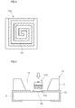
- Figs. 4 and 5 are views illustrating various examples of the convex portion 181 disposed on the light emitting chip.
- the convex portion 181 may have a lattice pattern shape in which a plurality of squares is arranged in a matrix.
- the convex portion 181 may have a spiral pattern shape.
- the convex portion 181 may have various shapes according to a design of the light emitting chip 100, but is not limited thereto.
- Fig. 6 is a view of a light emitting device according to a second invention.
- a light emitting device includes a body 11, a plurality of electrodes 31 and 32 disposed on the body 11, a package body 10 including a concave portion 36 disposed on at least one of the body 11 and the plurality of electrodes 31 and 32, and a light emitting chip 100 attached to the concave portion 36.
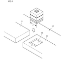
- Fig. 7 is a view illustrating a process of attaching the light emitting chip 10 to a package body.
- one concave portion 36 may have a shape corresponding to that of a lower surface of the light emitting chip 100.
- the concave portion may have an area (a) greater than or equal to that (c) of the lower surface of the light emitting chip 100.
- the concave portion 36 may have an area (a) equal to or greater by about 1.5 times than that (c) of the lower surface of the light emitting chip 100.
- the light emitting chip 100 Since the light emitting chip 100 is bonded and attached within the concave portion 36, it may prevent the light emitting chip 100 from being twisted due to an inner wall of the concave portion 36 when the light emitting chip 100 is bonded through eutectic bonding or bonding using an adhesive.
- the one concave portion 36 instead of the concave portion and convex portion of the first invention may be provided to prevent the light emitting chip 100 from being twisted during the bonding.
- the light emitting device manufacturing process may be simplified when compared to that in the first invention.
- Fig. 8 is a view of a light emitting device according to a third invention.
- a light emitting device includes a body 11, a plurality of electrodes 31 and 32 disposed on the body 11, a package body 10 including a concave portion 35 disposed on at least one of the plurality of electrodes 31 and 32, and a light emitting chip 200 including a convex portion 281 having a bottom surface thereof corresponding to the concave portion 35 and attached to the package body 10.
- Fig. 9 is a sectional view of a light emitting chip 200.
- the light emitting chip 200 may include a substrate 210, a first conductive type semiconductor layer 230 on the substrate 210, an active layer 240 on the first conductive type semiconductor layer 230, a second conductive type semiconductor layer 250 on the active layer 240, first and second electrode units 231 and 252 respectively disposed on the first and second conductive type semiconductor layers 230 and 250, and a reflective layer 205 including the convex portion 281 under the substrate 210.
- the substrate 210 may be formed of at least one of sapphire (A1 2 O 3 ), SiC, Si, GaAs, GaN, ZnO, Si, GaP, InP, and Ge, but is not limited thereto.
- the substrate 210 may include an insulating material.
- the first conductive type semiconductor layer 230, the active layer 240, and the second conductive type semiconductor layer 250 may be sequentially disposed on the substrate 210.
- a reflective layer 205 including the convex portion 281 may be disposed under the substrate 210.
- the reflective layer 205 may be formed of a metal having high reflective efficiency and including at least one of Ag, Al, Pd, Cu, and Pt or an alloy thereof.
- the light emitting chip 200 may be attached to the package body 10 through eutectic bonding or bonding using an adhesion layer such as an adhesive formed of a resin material.
- the reflective layer 205 may reflect light emitted from the active layer 240.
- the reflective layer 205 may not be provided.
- the convex portion 281 may be disposed on a lower surface of the substrate 210.
- an adhesion metal layer 206 may be further disposed on a lower surface of the reflective layer 205. Also, the convex portion 281 may be disposed on the adhesion metal layer 206, but is not limited thereto.
- the first and convex portions 35 and 281 may be respectively disposed on the package body 10 and the light emitting chip 200 to prevent the light emitting chip 200 from being twisted during the eutectic bonding or the bonding using the adhesion layer such as the adhesive formed of the resin material. Therefore, reliability of the light emitting device may be improved.
- Fig. 11 is view of a backlight unit using a light emitting device according to an invention.
- the backlight unit of Fig. 11 may be an example of a light unit, and thus, the present disclosure is not limited thereto.
- the backlight unit may include a bottom cover 1400, a light guide member 1100 disposed within the bottom cover 1400, and a light emitting module 1000 disposed on at least one side surface or a bottom surface of the light guide member 1100. Also, a reflective sheet 1300 may be disposed under the light guide member 1100.
- the bottom cover 1400 may have an upwardly opened box shape to receive the light guide member 1100, the light emitting module 1000, and the reflective sheet 1300. Also, the bottom cover 1400 may be formed of a metal material or a resin material, but is not limited thereto.
- the light emitting module 1000 may include a board and a plurality of light emitting devices mounted on the board.
- the plurality of light emitting devices according to an invention may provide light to the light guide member 1100.
- the light emitting module 1000 may be disposed on at least one of inner side surfaces of the bottom cover 1400, and thus, the light emitting module 1100 may provide light toward at least one side surface of the light guide member 1100.
- the light emitting module 1000 may be disposed on a bottom surface of the bottom cover 1400 to provide light toward a bottom surface of the light guide member 1100. Since this structure may be variously varied according to a design of the backlight unit, the present disclosure is not limited to the above-described structure.
- the light guide member 1100 may be disposed inside the bottom cover 1400.
- the light guide member 1100 may receive the light provided from the light emitting module 1000 to produce planar light, and then guide the planar light to a display panel (not shown).
- the light guide member 1100 may be a light guide panel (LGP).
- the light guide panel may be formed of one of an acryl-based material such as polymethylmethacrylate (PMMA), a polyethylene terephthalate (PET) resin, a poly carbonate (PC) resin, a cyclic olefin copolymer (COC) resin, and a polyethylene naphthalate (PEN) resin.
- PMMA polymethylmethacrylate
- PET polyethylene terephthalate
- PC poly carbonate
- COC cyclic olefin copolymer
- PEN polyethylene naphthalate
- the light guide member 1100 may include at least one of the light guide panel or the optical sheet.
- the optical sheet may include at least one of a diffusion sheet, a light collection sheet, and a brightness enhanced sheet.
- the diffusion sheet, the light collection sheet, and the brightness enhanced sheet may be sequentially stacked to form the optical sheet.
- the diffusion sheet may uniformly diffuse light emitted from the light emitting module 1000, and then the diffused light may be collected into the display panel (not shown) by the light collection sheet.
- the light emitted from the light collection sheet may be randomly polarized light.
- the bright enhanced sheet may enhance a degree of polarization of the light emitted from the light collection sheet.
- the light collection sheet may be a horizontal and/or vertical prism sheet.
- the bright enhanced sheet may be a dual brightness enhancement film.
- the reflective sheet 1300 may be disposed under the light guide member 1100.
- the reflective sheet 1300 may reflects the light emitted through the bottom surface of the light guide member 1100 toward a light emitting surface of the light guide member 1100.
- the reflective sheet 1300 may be formed of a material having superior reflectance, e.g., a PET resin, a PC resin, or a PVC resin, but is not limited thereto.
- Fig. 12 is a view of a lighting unit 1100 using a light emitting device 200 according to an invention.
- the lighting unit of Fig. 12 is an example of a light unit, but is not limited thereto.
- the lighting unit 1100 may include a case body 1110, a light emitting module 1130 disposed on the case body 1110, a connection terminal 1120 disposed on the case body 1110 to receive a power from an external power source.
- the case body 1110 may be formed of a material having good thermal dissipation properties, e.g., a metal material or a resin material.
- the light emitting module 1130 may include a board 1132 and at least one light emitting device 200 mounted on the board 1132.
- a circuit pattern may be printed on a dielectric to manufacture the board 1132.
- the board 1132 may include a printed circuit board (PCB), a metal core PCB, a flexible PCB, and a ceramic PCB.
- PCB printed circuit board
- metal core PCB metal core PCB
- flexible PCB flexible PCB
- ceramic PCB ceramic PCB
- the board 1132 may be formed of an effectively reflective material or have a color on which light is effectively reflected from a surface thereof, e.g., a white color or a silver color.
- At least one light emitting device 200 may be mounted on the board 1132.
- the light emitting device 200 may include at least one light emitting diode (LED).
- the LED may include color LEDs, which respectively emit light having a red color, a green color, a blue color, and a white color and an ultraviolet (UV) LED emitting UV rays.
- UV ultraviolet
- the light emitting module 1130 may have various combinations of the LEDs to obtain color impression and brightness.
- the white LED, the red LED, and the green LED may be combined with each other to secure a high color rendering index (CRI).
- CRI color rendering index
- connection terminal 1120 may be electrically connected to the light emitting module 1130 to provide a power to the light emitting module 1230.
- the connected terminal 1120 is screw-coupled to an external power source in a socket manner, but is not limited thereto.
- the connection terminal 1120 may have a pin shape, and thus, be inserted into the external power source.
- the connection terminal 1120 may be connected to the external power source by an interconnection.
- any reference in this specification to "one embodiment,” “an embodiment,” “example embodiment,” etc. means that a particular feature, structure, or characteristic described in connection with the embodiment is included in at least one embodiment of the invention.
- the appearances of such phrases in various places in the specification are not necessarily all referring to the same embodiment.
Landscapes
- Led Device Packages (AREA)
- Led Devices (AREA)
Applications Claiming Priority (1)
| Application Number | Priority Date | Filing Date | Title |
|---|---|---|---|
| KR1020100014161A KR100999736B1 (ko) | 2010-02-17 | 2010-02-17 | 발광 소자, 발광 소자 제조방법 및 라이트 유닛 |
Publications (3)
| Publication Number | Publication Date |
|---|---|
| EP2357681A2 true EP2357681A2 (fr) | 2011-08-17 |
| EP2357681A3 EP2357681A3 (fr) | 2014-09-10 |
| EP2357681B1 EP2357681B1 (fr) | 2017-07-19 |
Family
ID=43512604
Family Applications (1)
| Application Number | Title | Priority Date | Filing Date |
|---|---|---|---|
| EP11154427.6A Not-in-force EP2357681B1 (fr) | 2010-02-17 | 2011-02-14 | Dispositif électroluminescent et unité d'éclairage |
Country Status (5)
| Country | Link |
|---|---|
| US (1) | US8698185B2 (fr) |
| EP (1) | EP2357681B1 (fr) |
| KR (1) | KR100999736B1 (fr) |
| CN (1) | CN102194978B (fr) |
| TW (1) | TWI445220B (fr) |
Cited By (1)
| Publication number | Priority date | Publication date | Assignee | Title |
|---|---|---|---|---|
| EP2580792B1 (fr) * | 2010-06-10 | 2018-05-16 | OSRAM Opto Semiconductors GmbH | Corps semi-conducteur émetteur de rayonnement, procédé de fabrication d'un corps semi-conducteur émetteur de rayonnement et composant semi-conducteur émetteur de rayonnement |
Families Citing this family (10)
| Publication number | Priority date | Publication date | Assignee | Title |
|---|---|---|---|---|
| CN103811633B (zh) * | 2013-12-31 | 2017-05-10 | 江西鸿利光电有限公司 | 一种高可靠性发光二极管支架 |
| CN205564813U (zh) * | 2016-03-14 | 2016-09-07 | 京东方光科技有限公司 | 一种发光二极管装置及显示装置 |
| CN110792975A (zh) * | 2018-08-03 | 2020-02-14 | 汉能移动能源控股集团有限公司 | 灯带框架、灯带组件、型材、型材组件、拼接单元和路面系统 |
| CN109873060B (zh) * | 2019-04-18 | 2020-11-13 | 广东省半导体产业技术研究院 | 一种微发光二极管阵列制作方法 |
| CN110350061B (zh) * | 2019-07-10 | 2024-11-29 | 佛山市国星半导体技术有限公司 | 一种免用封装胶的led芯片、封装器件及封装方法 |
| KR102838438B1 (ko) * | 2019-11-25 | 2025-07-28 | 엘지전자 주식회사 | 마이크로 엘이디를 이용한 디스플레이 장치 |
| CN111725197B (zh) * | 2020-06-30 | 2022-06-03 | 上海天马微电子有限公司 | 微发光二极管基板及其制作方法、显示面板及其制作方法 |
| KR102721854B1 (ko) | 2020-11-26 | 2024-10-24 | 엘지디스플레이 주식회사 | 백라이트 유닛 및 그를 포함하는 표시 장치 |
| TWI820389B (zh) * | 2021-02-08 | 2023-11-01 | 隆達電子股份有限公司 | 發光元件封裝體、顯示裝置及製造顯示裝置的方法 |
| CN112859460B (zh) * | 2021-02-25 | 2022-10-04 | Tcl华星光电技术有限公司 | 显示装置、拼接显示装置以及绑定结构 |
Family Cites Families (16)
| Publication number | Priority date | Publication date | Assignee | Title |
|---|---|---|---|---|
| JP2004039983A (ja) | 2002-07-05 | 2004-02-05 | Rohm Co Ltd | 半導体発光装置 |
| US7015590B2 (en) | 2003-01-10 | 2006-03-21 | Samsung Electronics Co., Ltd. | Reinforced solder bump structure and method for forming a reinforced solder bump |
| JP4580633B2 (ja) * | 2003-11-14 | 2010-11-17 | スタンレー電気株式会社 | 半導体装置及びその製造方法 |
| JP2005203448A (ja) * | 2004-01-13 | 2005-07-28 | Toyoda Gosei Co Ltd | 発光装置 |
| WO2005091383A1 (fr) * | 2004-03-24 | 2005-09-29 | Renesas Yanai Semiconductor Inc. | Méthode de fabrication d'un dispositif émetteur de lumière et dispositif émetteur de lumière |
| JP4891556B2 (ja) * | 2005-03-24 | 2012-03-07 | 株式会社東芝 | 半導体装置の製造方法 |
| KR100755658B1 (ko) * | 2006-03-09 | 2007-09-04 | 삼성전기주식회사 | 발광다이오드 패키지 |
| JP4793169B2 (ja) * | 2006-08-24 | 2011-10-12 | 日立電線株式会社 | 接続体および光送受信モジュール |
| TWI318013B (en) | 2006-09-05 | 2009-12-01 | Epistar Corp | A light emitting device and the manufacture method thereof |
| JP2008091862A (ja) | 2006-09-08 | 2008-04-17 | Sharp Corp | 窒化物半導体発光素子および窒化物半導体発光素子の製造方法 |
| KR20080041794A (ko) | 2006-11-08 | 2008-05-14 | 삼성전기주식회사 | 발광 다이오드 패키지 |
| KR20090039261A (ko) | 2007-10-18 | 2009-04-22 | 삼성전기주식회사 | 발광다이오드 패키지 |
| KR101438826B1 (ko) | 2008-06-23 | 2014-09-05 | 엘지이노텍 주식회사 | 발광장치 |
| KR101103882B1 (ko) * | 2008-11-17 | 2012-01-12 | 엘지이노텍 주식회사 | 반도체 발광소자 및 그 제조방법 |
| KR101092063B1 (ko) | 2009-04-28 | 2011-12-12 | 엘지이노텍 주식회사 | 발광소자 패키지 및 그 제조방법 |
| TWM374006U (en) | 2009-08-26 | 2010-02-11 | Tse Jie Entpr Ltd | A modularized LED lighting device |
-
2010
- 2010-02-17 KR KR1020100014161A patent/KR100999736B1/ko not_active Expired - Fee Related
-
2011
- 2011-02-14 EP EP11154427.6A patent/EP2357681B1/fr not_active Not-in-force
- 2011-02-15 TW TW100104883A patent/TWI445220B/zh not_active IP Right Cessation
- 2011-02-15 US US13/027,949 patent/US8698185B2/en active Active
- 2011-02-17 CN CN2011100411626A patent/CN102194978B/zh not_active Expired - Fee Related
Non-Patent Citations (1)
| Title |
|---|
| None |
Cited By (1)
| Publication number | Priority date | Publication date | Assignee | Title |
|---|---|---|---|---|
| EP2580792B1 (fr) * | 2010-06-10 | 2018-05-16 | OSRAM Opto Semiconductors GmbH | Corps semi-conducteur émetteur de rayonnement, procédé de fabrication d'un corps semi-conducteur émetteur de rayonnement et composant semi-conducteur émetteur de rayonnement |
Also Published As
| Publication number | Publication date |
|---|---|
| US8698185B2 (en) | 2014-04-15 |
| TW201143171A (en) | 2011-12-01 |
| CN102194978B (zh) | 2013-10-23 |
| EP2357681B1 (fr) | 2017-07-19 |
| CN102194978A (zh) | 2011-09-21 |
| TWI445220B (zh) | 2014-07-11 |
| KR100999736B1 (ko) | 2010-12-08 |
| EP2357681A3 (fr) | 2014-09-10 |
| US20110198659A1 (en) | 2011-08-18 |
Similar Documents
| Publication | Publication Date | Title |
|---|---|---|
| EP2357681B1 (fr) | Dispositif électroluminescent et unité d'éclairage | |
| US9048377B2 (en) | Light emitting device, method for fabricating the light emitting device, light emitting device package, and lighting unit | |
| US8916887B2 (en) | Light emitting device package and lighting system using the same | |
| US8698176B2 (en) | Light emitting device and lighting system | |
| EP2369648A2 (fr) | Dispositif électroluminescent | |
| KR101762787B1 (ko) | 발광소자, 발광소자 패키지 및 조명 시스템 | |
| KR101824011B1 (ko) | 발광소자 패키지 | |
| JP2011187957A (ja) | 発光素子および発光素子の製造方法 | |
| EP2858127B1 (fr) | Diode électroluminescente | |
| CN102969415B (zh) | 发光器件 | |
| EP2365545B1 (fr) | Dispositif électroluminescent, emballage de dispositif électroluminescent et système d'éclairage | |
| US8350274B2 (en) | Light emitting device, method of manufacturing the light emitting device, light emitting device package, and lighting unit | |
| KR102187501B1 (ko) | 발광 소자 및 그를 포함하는 발광소자 패키지 | |
| KR20140099075A (ko) | 발광소자 | |
| KR20150017241A (ko) | 발광소자 | |
| KR102119851B1 (ko) | 발광소자 | |
| KR20140090282A (ko) | 발광소자 | |
| KR101028242B1 (ko) | 발광 소자 및 이를 이용한 라이트 유닛 | |
| KR102187480B1 (ko) | 발광 소자 및 발광소자 제조방법 | |
| KR102249628B1 (ko) | 발광소자 패키지 | |
| KR20140096654A (ko) | 발광 소자 및 그를 포함하는 발광소자 패키지 | |
| KR102019835B1 (ko) | 발광소자 | |
| KR101807111B1 (ko) | 발광 소자 및 그 제조방법 | |
| KR20140097605A (ko) | 발광 소자 및 그를 포함하는 발광소자 패키지 | |
| KR20140099071A (ko) | 발광소자 |
Legal Events
| Date | Code | Title | Description |
|---|---|---|---|
| PUAI | Public reference made under article 153(3) epc to a published international application that has entered the european phase |
Free format text: ORIGINAL CODE: 0009012 |
|
| 17P | Request for examination filed |
Effective date: 20110214 |
|
| AK | Designated contracting states |
Kind code of ref document: A2 Designated state(s): AL AT BE BG CH CY CZ DE DK EE ES FI FR GB GR HR HU IE IS IT LI LT LU LV MC MK MT NL NO PL PT RO RS SE SI SK SM TR |
|
| AX | Request for extension of the european patent |
Extension state: BA ME |
|
| RAP1 | Party data changed (applicant data changed or rights of an application transferred) |
Owner name: LG INNOTEK CO., LTD. |
|
| PUAL | Search report despatched |
Free format text: ORIGINAL CODE: 0009013 |
|
| AK | Designated contracting states |
Kind code of ref document: A3 Designated state(s): AL AT BE BG CH CY CZ DE DK EE ES FI FR GB GR HR HU IE IS IT LI LT LU LV MC MK MT NL NO PL PT RO RS SE SI SK SM TR |
|
| AX | Request for extension of the european patent |
Extension state: BA ME |
|
| RIC1 | Information provided on ipc code assigned before grant |
Ipc: H01L 33/38 20100101AFI20140801BHEP Ipc: H01L 33/20 20100101ALI20140801BHEP Ipc: H01L 33/62 20100101ALN20140801BHEP |
|
| RBV | Designated contracting states (corrected) |
Designated state(s): AL AT BE BG CH CY CZ DE DK EE ES FI FR GB GR HR HU IE IS IT LI LT LU LV MC MK MT NL NO PL PT RO RS SE SI SK SM TR |
|
| 17Q | First examination report despatched |
Effective date: 20160711 |
|
| GRAP | Despatch of communication of intention to grant a patent |
Free format text: ORIGINAL CODE: EPIDOSNIGR1 |
|
| STAA | Information on the status of an ep patent application or granted ep patent |
Free format text: STATUS: GRANT OF PATENT IS INTENDED |
|
| RIC1 | Information provided on ipc code assigned before grant |
Ipc: H01L 33/20 20100101ALI20161212BHEP Ipc: H01L 33/62 20100101ALN20161212BHEP Ipc: H01L 33/38 20100101AFI20161212BHEP |
|
| INTG | Intention to grant announced |
Effective date: 20170103 |
|
| GRAS | Grant fee paid |
Free format text: ORIGINAL CODE: EPIDOSNIGR3 |
|
| RAP1 | Party data changed (applicant data changed or rights of an application transferred) |
Owner name: LG INNOTEK CO., LTD. |
|
| GRAA | (expected) grant |
Free format text: ORIGINAL CODE: 0009210 |
|
| STAA | Information on the status of an ep patent application or granted ep patent |
Free format text: STATUS: THE PATENT HAS BEEN GRANTED |
|
| AK | Designated contracting states |
Kind code of ref document: B1 Designated state(s): AL AT BE BG CH CY CZ DE DK EE ES FI FR GB GR HR HU IE IS IT LI LT LU LV MC MK MT NL NO PL PT RO RS SE SI SK SM TR |
|
| REG | Reference to a national code |
Ref country code: GB Ref legal event code: FG4D |
|
| REG | Reference to a national code |
Ref country code: CH Ref legal event code: EP |
|
| REG | Reference to a national code |
Ref country code: IE Ref legal event code: FG4D |
|
| REG | Reference to a national code |
Ref country code: AT Ref legal event code: REF Ref document number: 911152 Country of ref document: AT Kind code of ref document: T Effective date: 20170815 |
|
| REG | Reference to a national code |
Ref country code: DE Ref legal event code: R096 Ref document number: 602011039625 Country of ref document: DE |
|
| REG | Reference to a national code |
Ref country code: NL Ref legal event code: MP Effective date: 20170719 |
|
| REG | Reference to a national code |
Ref country code: LT Ref legal event code: MG4D |
|
| REG | Reference to a national code |
Ref country code: AT Ref legal event code: MK05 Ref document number: 911152 Country of ref document: AT Kind code of ref document: T Effective date: 20170719 |
|
| PG25 | Lapsed in a contracting state [announced via postgrant information from national office to epo] |
Ref country code: AT Free format text: LAPSE BECAUSE OF FAILURE TO SUBMIT A TRANSLATION OF THE DESCRIPTION OR TO PAY THE FEE WITHIN THE PRESCRIBED TIME-LIMIT Effective date: 20170719 Ref country code: SE Free format text: LAPSE BECAUSE OF FAILURE TO SUBMIT A TRANSLATION OF THE DESCRIPTION OR TO PAY THE FEE WITHIN THE PRESCRIBED TIME-LIMIT Effective date: 20170719 Ref country code: HR Free format text: LAPSE BECAUSE OF FAILURE TO SUBMIT A TRANSLATION OF THE DESCRIPTION OR TO PAY THE FEE WITHIN THE PRESCRIBED TIME-LIMIT Effective date: 20170719 Ref country code: NO Free format text: LAPSE BECAUSE OF FAILURE TO SUBMIT A TRANSLATION OF THE DESCRIPTION OR TO PAY THE FEE WITHIN THE PRESCRIBED TIME-LIMIT Effective date: 20171019 Ref country code: NL Free format text: LAPSE BECAUSE OF FAILURE TO SUBMIT A TRANSLATION OF THE DESCRIPTION OR TO PAY THE FEE WITHIN THE PRESCRIBED TIME-LIMIT Effective date: 20170719 Ref country code: FI Free format text: LAPSE BECAUSE OF FAILURE TO SUBMIT A TRANSLATION OF THE DESCRIPTION OR TO PAY THE FEE WITHIN THE PRESCRIBED TIME-LIMIT Effective date: 20170719 Ref country code: LT Free format text: LAPSE BECAUSE OF FAILURE TO SUBMIT A TRANSLATION OF THE DESCRIPTION OR TO PAY THE FEE WITHIN THE PRESCRIBED TIME-LIMIT Effective date: 20170719 |
|
| PG25 | Lapsed in a contracting state [announced via postgrant information from national office to epo] |
Ref country code: GR Free format text: LAPSE BECAUSE OF FAILURE TO SUBMIT A TRANSLATION OF THE DESCRIPTION OR TO PAY THE FEE WITHIN THE PRESCRIBED TIME-LIMIT Effective date: 20171020 Ref country code: LV Free format text: LAPSE BECAUSE OF FAILURE TO SUBMIT A TRANSLATION OF THE DESCRIPTION OR TO PAY THE FEE WITHIN THE PRESCRIBED TIME-LIMIT Effective date: 20170719 Ref country code: RS Free format text: LAPSE BECAUSE OF FAILURE TO SUBMIT A TRANSLATION OF THE DESCRIPTION OR TO PAY THE FEE WITHIN THE PRESCRIBED TIME-LIMIT Effective date: 20170719 Ref country code: ES Free format text: LAPSE BECAUSE OF FAILURE TO SUBMIT A TRANSLATION OF THE DESCRIPTION OR TO PAY THE FEE WITHIN THE PRESCRIBED TIME-LIMIT Effective date: 20170719 Ref country code: IS Free format text: LAPSE BECAUSE OF FAILURE TO SUBMIT A TRANSLATION OF THE DESCRIPTION OR TO PAY THE FEE WITHIN THE PRESCRIBED TIME-LIMIT Effective date: 20171119 Ref country code: BG Free format text: LAPSE BECAUSE OF FAILURE TO SUBMIT A TRANSLATION OF THE DESCRIPTION OR TO PAY THE FEE WITHIN THE PRESCRIBED TIME-LIMIT Effective date: 20171019 Ref country code: PL Free format text: LAPSE BECAUSE OF FAILURE TO SUBMIT A TRANSLATION OF THE DESCRIPTION OR TO PAY THE FEE WITHIN THE PRESCRIBED TIME-LIMIT Effective date: 20170719 |
|
| REG | Reference to a national code |
Ref country code: DE Ref legal event code: R097 Ref document number: 602011039625 Country of ref document: DE |
|
| PG25 | Lapsed in a contracting state [announced via postgrant information from national office to epo] |
Ref country code: RO Free format text: LAPSE BECAUSE OF FAILURE TO SUBMIT A TRANSLATION OF THE DESCRIPTION OR TO PAY THE FEE WITHIN THE PRESCRIBED TIME-LIMIT Effective date: 20170719 Ref country code: CZ Free format text: LAPSE BECAUSE OF FAILURE TO SUBMIT A TRANSLATION OF THE DESCRIPTION OR TO PAY THE FEE WITHIN THE PRESCRIBED TIME-LIMIT Effective date: 20170719 Ref country code: DK Free format text: LAPSE BECAUSE OF FAILURE TO SUBMIT A TRANSLATION OF THE DESCRIPTION OR TO PAY THE FEE WITHIN THE PRESCRIBED TIME-LIMIT Effective date: 20170719 |
|
| PLBE | No opposition filed within time limit |
Free format text: ORIGINAL CODE: 0009261 |
|
| STAA | Information on the status of an ep patent application or granted ep patent |
Free format text: STATUS: NO OPPOSITION FILED WITHIN TIME LIMIT |
|
| PG25 | Lapsed in a contracting state [announced via postgrant information from national office to epo] |
Ref country code: SK Free format text: LAPSE BECAUSE OF FAILURE TO SUBMIT A TRANSLATION OF THE DESCRIPTION OR TO PAY THE FEE WITHIN THE PRESCRIBED TIME-LIMIT Effective date: 20170719 Ref country code: EE Free format text: LAPSE BECAUSE OF FAILURE TO SUBMIT A TRANSLATION OF THE DESCRIPTION OR TO PAY THE FEE WITHIN THE PRESCRIBED TIME-LIMIT Effective date: 20170719 Ref country code: SM Free format text: LAPSE BECAUSE OF FAILURE TO SUBMIT A TRANSLATION OF THE DESCRIPTION OR TO PAY THE FEE WITHIN THE PRESCRIBED TIME-LIMIT Effective date: 20170719 Ref country code: IT Free format text: LAPSE BECAUSE OF FAILURE TO SUBMIT A TRANSLATION OF THE DESCRIPTION OR TO PAY THE FEE WITHIN THE PRESCRIBED TIME-LIMIT Effective date: 20170719 |
|
| 26N | No opposition filed |
Effective date: 20180420 |
|
| PG25 | Lapsed in a contracting state [announced via postgrant information from national office to epo] |
Ref country code: SI Free format text: LAPSE BECAUSE OF FAILURE TO SUBMIT A TRANSLATION OF THE DESCRIPTION OR TO PAY THE FEE WITHIN THE PRESCRIBED TIME-LIMIT Effective date: 20170719 |
|
| REG | Reference to a national code |
Ref country code: CH Ref legal event code: PL |
|
| PG25 | Lapsed in a contracting state [announced via postgrant information from national office to epo] |
Ref country code: MC Free format text: LAPSE BECAUSE OF FAILURE TO SUBMIT A TRANSLATION OF THE DESCRIPTION OR TO PAY THE FEE WITHIN THE PRESCRIBED TIME-LIMIT Effective date: 20170719 |
|
| REG | Reference to a national code |
Ref country code: IE Ref legal event code: MM4A |
|
| REG | Reference to a national code |
Ref country code: BE Ref legal event code: MM Effective date: 20180228 |
|
| PG25 | Lapsed in a contracting state [announced via postgrant information from national office to epo] |
Ref country code: CH Free format text: LAPSE BECAUSE OF NON-PAYMENT OF DUE FEES Effective date: 20180228 Ref country code: LU Free format text: LAPSE BECAUSE OF NON-PAYMENT OF DUE FEES Effective date: 20180214 Ref country code: LI Free format text: LAPSE BECAUSE OF NON-PAYMENT OF DUE FEES Effective date: 20180228 |
|
| REG | Reference to a national code |
Ref country code: FR Ref legal event code: ST Effective date: 20181031 |
|
| PG25 | Lapsed in a contracting state [announced via postgrant information from national office to epo] |
Ref country code: IE Free format text: LAPSE BECAUSE OF NON-PAYMENT OF DUE FEES Effective date: 20180214 |
|
| PG25 | Lapsed in a contracting state [announced via postgrant information from national office to epo] |
Ref country code: FR Free format text: LAPSE BECAUSE OF NON-PAYMENT OF DUE FEES Effective date: 20180228 Ref country code: BE Free format text: LAPSE BECAUSE OF NON-PAYMENT OF DUE FEES Effective date: 20180228 |
|
| PG25 | Lapsed in a contracting state [announced via postgrant information from national office to epo] |
Ref country code: MT Free format text: LAPSE BECAUSE OF NON-PAYMENT OF DUE FEES Effective date: 20180214 |
|
| PG25 | Lapsed in a contracting state [announced via postgrant information from national office to epo] |
Ref country code: TR Free format text: LAPSE BECAUSE OF FAILURE TO SUBMIT A TRANSLATION OF THE DESCRIPTION OR TO PAY THE FEE WITHIN THE PRESCRIBED TIME-LIMIT Effective date: 20170719 |
|
| PG25 | Lapsed in a contracting state [announced via postgrant information from national office to epo] |
Ref country code: PT Free format text: LAPSE BECAUSE OF FAILURE TO SUBMIT A TRANSLATION OF THE DESCRIPTION OR TO PAY THE FEE WITHIN THE PRESCRIBED TIME-LIMIT Effective date: 20170719 Ref country code: HU Free format text: LAPSE BECAUSE OF FAILURE TO SUBMIT A TRANSLATION OF THE DESCRIPTION OR TO PAY THE FEE WITHIN THE PRESCRIBED TIME-LIMIT; INVALID AB INITIO Effective date: 20110214 |
|
| PG25 | Lapsed in a contracting state [announced via postgrant information from national office to epo] |
Ref country code: CY Free format text: LAPSE BECAUSE OF FAILURE TO SUBMIT A TRANSLATION OF THE DESCRIPTION OR TO PAY THE FEE WITHIN THE PRESCRIBED TIME-LIMIT Effective date: 20170719 Ref country code: MK Free format text: LAPSE BECAUSE OF NON-PAYMENT OF DUE FEES Effective date: 20170719 |
|
| PG25 | Lapsed in a contracting state [announced via postgrant information from national office to epo] |
Ref country code: AL Free format text: LAPSE BECAUSE OF FAILURE TO SUBMIT A TRANSLATION OF THE DESCRIPTION OR TO PAY THE FEE WITHIN THE PRESCRIBED TIME-LIMIT Effective date: 20170719 |
|
| REG | Reference to a national code |
Ref country code: GB Ref legal event code: 732E Free format text: REGISTERED BETWEEN 20210722 AND 20210728 |
|
| REG | Reference to a national code |
Ref country code: DE Ref legal event code: R081 Ref document number: 602011039625 Country of ref document: DE Owner name: SUZHOU LEKIN SEMICONDUCTOR CO. LTD., TAICANG, CN Free format text: FORMER OWNER: LG INNOTEK CO., LTD., SEOUL, KR |
|
| PGFP | Annual fee paid to national office [announced via postgrant information from national office to epo] |
Ref country code: GB Payment date: 20231221 Year of fee payment: 14 |
|
| PGFP | Annual fee paid to national office [announced via postgrant information from national office to epo] |
Ref country code: DE Payment date: 20231220 Year of fee payment: 14 |
|
| REG | Reference to a national code |
Ref country code: DE Ref legal event code: R079 Ref document number: 602011039625 Country of ref document: DE Free format text: PREVIOUS MAIN CLASS: H01L0033380000 Ipc: H10H0020831000 |
|
| REG | Reference to a national code |
Ref country code: DE Ref legal event code: R119 Ref document number: 602011039625 Country of ref document: DE |
|
| GBPC | Gb: european patent ceased through non-payment of renewal fee |
Effective date: 20250214 |
|
| PG25 | Lapsed in a contracting state [announced via postgrant information from national office to epo] |
Ref country code: DE Free format text: LAPSE BECAUSE OF NON-PAYMENT OF DUE FEES Effective date: 20250902 |
|
| PG25 | Lapsed in a contracting state [announced via postgrant information from national office to epo] |
Ref country code: GB Free format text: LAPSE BECAUSE OF NON-PAYMENT OF DUE FEES Effective date: 20250214 |