EP2360809B1 - Réseau de distribution d'énergie basé sur des composants de stockage à charge multiple - Google Patents
Réseau de distribution d'énergie basé sur des composants de stockage à charge multiple Download PDFInfo
- Publication number
- EP2360809B1 EP2360809B1 EP10153698.5A EP10153698A EP2360809B1 EP 2360809 B1 EP2360809 B1 EP 2360809B1 EP 10153698 A EP10153698 A EP 10153698A EP 2360809 B1 EP2360809 B1 EP 2360809B1
- Authority
- EP
- European Patent Office
- Prior art keywords
- power
- battery
- distribution network
- terminal
- charge storage
- Prior art date
- Legal status (The legal status is an assumption and is not a legal conclusion. Google has not performed a legal analysis and makes no representation as to the accuracy of the status listed.)
- Active
Links
Images



Classifications
-
- H—ELECTRICITY
- H02—GENERATION; CONVERSION OR DISTRIBUTION OF ELECTRIC POWER
- H02J—ELECTRIC POWER NETWORKS; CIRCUIT ARRANGEMENTS OR SYSTEMS FOR SUPPLYING OR DISTRIBUTING ELECTRIC POWER; SYSTEMS FOR STORING ELECTRIC ENERGY
- H02J7/00—Circuit arrangements for charging or discharging batteries or for supplying loads from batteries
- H02J7/34—Parallel operation in networks using both storage and other DC sources, e.g. providing buffering
- H02J7/345—Parallel operation in networks using both storage and other DC sources, e.g. providing buffering using capacitors as storage or buffering devices
-
- H—ELECTRICITY
- H02—GENERATION; CONVERSION OR DISTRIBUTION OF ELECTRIC POWER
- H02M—APPARATUS FOR CONVERSION BETWEEN AC AND AC, BETWEEN AC AND DC, OR BETWEEN DC AND DC, AND FOR USE WITH MAINS OR SIMILAR POWER SUPPLY SYSTEMS; CONVERSION OF DC OR AC INPUT POWER INTO SURGE OUTPUT POWER; CONTROL OR REGULATION THEREOF
- H02M3/00—Conversion of DC power input into DC power output
- H02M3/02—Conversion of DC power input into DC power output without intermediate conversion into AC
- H02M3/04—Conversion of DC power input into DC power output without intermediate conversion into AC by static converters
- H02M3/10—Conversion of DC power input into DC power output without intermediate conversion into AC by static converters using discharge tubes with control electrode or semiconductor devices with control electrode
- H02M3/145—Conversion of DC power input into DC power output without intermediate conversion into AC by static converters using discharge tubes with control electrode or semiconductor devices with control electrode using devices of a triode or transistor type requiring continuous application of a control signal
- H02M3/155—Conversion of DC power input into DC power output without intermediate conversion into AC by static converters using discharge tubes with control electrode or semiconductor devices with control electrode using devices of a triode or transistor type requiring continuous application of a control signal using semiconductor devices only
- H02M3/156—Conversion of DC power input into DC power output without intermediate conversion into AC by static converters using discharge tubes with control electrode or semiconductor devices with control electrode using devices of a triode or transistor type requiring continuous application of a control signal using semiconductor devices only with automatic control of output voltage or current, e.g. switching regulators
-
- H—ELECTRICITY
- H02—GENERATION; CONVERSION OR DISTRIBUTION OF ELECTRIC POWER
- H02J—ELECTRIC POWER NETWORKS; CIRCUIT ARRANGEMENTS OR SYSTEMS FOR SUPPLYING OR DISTRIBUTING ELECTRIC POWER; SYSTEMS FOR STORING ELECTRIC ENERGY
- H02J2207/00—Details of circuit arrangements for charging or discharging batteries or supplying loads from batteries
- H02J2207/20—Charging or discharging characterised by the power electronics converter
Definitions
- the present application relates generally to power distribution networks and, more specifically, to a power distribution network based on multiple charge storage components.
- ripple in the power supply voltage may result from pulsed high-current draw by, for example, a radio frequency power amplifier circuit. Propagation of the ripple to other components relying on the power distribution network may cause undesirable effects. For an audio circuit, for example, the ripple may cause an audible buzz. Additionally, certain arrangements of the power pack relative to the power amplifier circuit may allow for generation of significant electromagnetic interference.
- US 5587250 discloses a related art power distribution network.
- power supply ripple may be reduced by buffering, at a secondary charge storage component, a pulsed high current that the power amplifier circuit may draw from the primary power supply.
- a power distribution network as recited in claim 1.
- FIG. 1 illustrates a power distribution network 100 with a power amplifier circuit 124 and a power pack 120.
- the power pack 120 includes at least one charge storage component.
- the charge storage component may be any component that stores electrical charge, such as a chemical power cell or a supercapacitor.
- the power distribution network 100 is arranged for use in a mobile communication device.
- the mobile communication device includes a processor 102 for controlling the overall operation of the mobile communication device, or for controlling selected operations of the mobile communication device.
- Components of the mobile communication device include a housing (not shown) and multiple user interface components 104.
- the user interface components 104 may include an input device (e.g., a keyboard having a plurality of keys, a button, a trackball or touchpad) and an output device (e.g., a display), which may comprise a full graphic, or full color, Liquid Crystal Display (LCD).
- the display may comprise a touchscreen display.
- the keyboard may comprise a virtual keyboard.
- Other types of output devices may alternatively be utilized.
- the processor 102 controls the operation of the display, in part, responsive to actuation of the keys on the keyboard by a user of the mobile communication device.
- Components of the mobile communication device may also include an audio circuit 106, which may control presentation, to the user, of an audio alert (a ring tone), audio received in a telephone call and audio based on a digital music file saved in device memory (not shown).
- an audio alert a ring tone
- audio received in a telephone call and audio based on a digital music file saved in device memory (not shown).
- Components of the mobile communication device may also include a receiver 108 for use with the known global positioning system (GPS).
- GPS global positioning system
- the GPS receiver 108 is illustrated as being communicatively connected to a GPS receiver antenna 118A.
- Components of the mobile communication device may also include a transceiver 110 for use in a short-range communications subsystem that enables communication between the mobile communication device and other proximate systems or devices, which need not necessarily be similar devices.
- the short-range communications subsystem may include an infrared device and associated circuits and components, or a BluetoothTM communication module to provide for communication with similarly-enabled systems and devices.
- the Bluetooth transceiver 110 is illustrated as being communicatively connected to a Bluetooth transceiver antenna 118B.
- Components of the mobile communication device may also include a transceiver 112 for use in a wireless local area networking communication subsystem.
- a set of standards has been established by the Institute of Electrical and Electronics Engineers (IEEE) and is known as IEEE 802.11 standards. Products may be certified by the known Wi-Fi Alliance for adherence to the IEEE 802.11 standards.
- the Wi-Fi transceiver 112 is illustrated as being communicatively connected to a Wi-Fi transceiver antenna 118C.
- Components of the mobile communication device may also include a transceiver 114 for use in a first wireless telecommunication subsystem.
- the first wireless telecommunication subsystem may be based on the known Wideband Code Division Multiple Access (W-CDMA) standard.
- W-CDMA Wideband Code Division Multiple Access
- the W-CDMA transceiver 114 is illustrated as being communicatively connected to a W-CDMA transceiver antenna 118D.
- Components of the mobile communication device may also include a transceiver 116 for use in a second wireless telecommunication subsystem.
- the second wireless telecommunication subsystem may be based on the known Global System for Mobile communications (GSM) and Enhanced Data rates for GSM Evolution (EDGE) standards.
- GSM Global System for Mobile communications
- EDGE Enhanced Data rates for GSM Evolution
- the GSM/EDGE transceiver 116 is illustrated as being communicatively connected, through the power amplifier circuit 124, to a GSM/EDGE transceiver antenna 118E.
- the processor 102, the user interfaces 104, the audio circuit 106, the GPS receiver 108, the Bluetooth transceiver 110, the Wi-Fi transceiver 112, the W-CDMA transceiver 114 and the GSM/EDGE transceiver 116 all maintain a connection to a power management integrated circuit (PMIC) 122.
- PMIC power management integrated circuit
- the PMIC 122 and the power amplifier circuit 124 maintain a connection to the power pack 120.
- the power pack 120 through a first terminal 132A, maintains a connection to the PMIC 122 and to a battery charging circuit 126.
- the power pack 120 through a second terminal 134A, maintains a connection to a power supply reference voltage in common with components of the power amplifier circuit 124.
- Another pair of terminals includes a third terminal 132B connecting the power pack 120, through a step-down direct current to direct current (DC-to-DC) converter 128, to the power amplifier circuit 124 and a fourth terminal 134B connecting the power pack 120 to the power supply reference voltage.
- DC-to-DC direct current to direct current
- the step-down DC-to-DC converter 128 receives, at an input terminal, the voltage available at the third terminal 132A of the power pack 120, converts the voltage received at the input terminal to a lower voltage and makes the lower voltage available, at an output terminal, to the power amplifier circuit 124.
- the power pack 120 may, for example, house a Li-lon battery with an operational range of from 4.2V to 3.2V.
- the concepts described herein are not limited, however, to any particular form of energy storage or battery chemistry.
- the power amplifier circuit 124 includes (but is not necessarily limited to) a power amplifier 202 that connects to an output of the GSM/EDGE transceiver 116 and to an input to a low pass filter 204.
- a switch 206 connects, in one state, the output of the low pass filter 204 to an antenna matching circuit 208, which connects to the GSM/EDGE transceiver antenna 118E. In another state, switch 206 connects the output of the antenna matching circuit 208 to an input of a band pass filter 210. The output of the band pass filter 210 connects to an input of the GSM/EDGE transceiver 116.
- the power amplifier 202 is illustrated as comprising multiple stages (not individually referenced) with each stage receiving a power supply voltage from a first terminal 212A of the power pack 120. Similarly, each stage shares power supply reference voltage with a second terminal 214A of the power pack 120.
- the GSM/EDGE transceiver 116 may cause the power amplifier 202 to be operated in a so-called "pulse mode".
- the pulse mode of power amplifier operation is known to cause variation in the power supply voltage provided at the first terminal 212 of the power pack 120.
- the variation, or ripple, in the power supply voltage may be as much as 400mV peak-to-peak due to high pulsed current.
- the ripple may propagate from the power pack 120, to the PMIC 122, to the rest of the components.
- the ripple may cause an audible buzz (for GSM-based communication devices, many have experienced a buzz at 217Hz), elimination of which has been perceived as difficult and costly.
- the efficiency of the power amplifier 202 is generally maintained by a stable supply voltage.
- the power supply voltage provided at the third terminal 132B of the power pack 120 can change, as the charge on the charge storage component is diminished, from 4.2V (fully charged) to as low as 3.2V (needing recharge). Indeed, when the charge on the charge storage component has been reduced and the power supply voltage provided at the third terminal 132B of the power pack 120 is correspondingly reduced, the power amplifier 202 may be forced into an undesired saturation mode.
- the power level of the radio frequency (RF) signal output to the GSM/EDGE transceiver antenna 118E is reduced relative to a preferred power level. Additionally, it may be considered that operation of the power amplifier 202 in saturation mode compromises the output spectrum.
- RF radio frequency
- design sacrifices or accommodations are required to be made.
- design sacrifices may include the addition of circuits designed to control the behavior of the power amplifier 202 under reduced supply voltage.
- One such circuit is known as an anti-saturation loop.
- additional circuits may be considered to increase the complexity and cost of the power amplifier 202.
- a power amplifier current loop may be defined as being formed through the power pack 120 and the power amplifier 202. With the relatively large area of the loop, it may be shown that the pulse mode of power amplifier operation causes measurable magnetic radiation to be emitted. This emission may be shown to interfere with other circuits, such as the circuits found in hearing aids, especially among the circuits found in hearing aids that utilize a T-magnetic coil (or T-coil) to pick up an audio signal. The emission of magnetic radiation from the power amplifier current loop can also be problematic when the radiation couples to various transducers and other components within the enclosure of the mobile communication device to which the power distribution network 100 provides power.
- Radio Frequency (RF) interference signals (any unwanted signals) that are present at the power amplifier 202 during transmission may be coupled to other circuits 104, 106, 108, 110, 112, 114, 116, 122, 126 via the power supply lines. If the interference signals become coupled to the battery housed by the power pack 120, for example, it can be shown that those interference signals may be radiated by the battery due to the charge storage component structure.
- the charge storage component structure may, for example, involve the third terminal 132B (i.e., the positive contact) of the power pack 120 being connected to the mobile communication device housing. In such a case, it may be shown that the mobile communication device housing may behave like an antenna.
- power supply ripple may be reduced by buffering, at a secondary power supply, a pulsed high current that the power amplifier circuit may draw from the primary power supply.
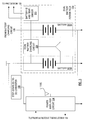
- FIG. 3 illustrates the power amplifier circuit 124 as supplied with power by multiple charge storage components.
- the multiple charge storage components are provided in a dual battery power pack 320.
- the dual battery power pack 320 includes a first battery 322A and a second battery 322B.
- the first battery 322A has a first terminal connected to the battery charging circuit 126 and a second terminal connected to a common supply voltage for the power distribution network.
- a second terminal of the second battery 322B is also connected to the common supply voltage for the power distribution network.
- a first terminal of the second battery 322B and the first terminal of the first battery 322A are connected to, and interposed by, a dual-battery charging circuit 321. While the battery charging circuit 126 may be considered to be a "primary" charging circuit, the dual-battery charging circuit 321 may be considered to be a "secondary" charging circuit.
- the power amplifier circuit 124 of FIG. 3 is arranged to receive a signal from the GSM/EDGE transceiver 116 for transmission on the GSM/EDGE transceiver antenna 118E. Additionally, the power amplifier circuit 124 of FIG. 3 is arranged to receive a signal from the GSM/EDGE transceiver antenna 118E and transmit the received signal to the GSM/EDGE transceiver 116.
- the dual battery power pack 320 includes a battery identifier and temperature sensor 326.
- the battery identifier and temperature sensor 326 connects to the processor 102 ( FIG. 1 ).
- the battery identifier portion is adapted to output an identification of the dual battery power pack 320.
- the temperature sensor portion is adapted to sense a temperature within the dual battery power pack 320 and provide an output signal indicative of the temperature to the processor 102.
- the dual-battery charging circuit 321 can act to continuously charge the second battery 322B, thereby maintaining a more consistent charge on the second battery 322B than would be possible with a single-battery power pack. Consequently, the power amplifier circuit 124 of FIG. 3 may be designed to take advantage of a consistent voltage at the output of the step-down DC-to-DC converter 128 in a manner unavailable to the designer of the power amplifier circuit 124 of FIG. 1 .
- ESR Equivalent Series Resistance
- the power amplifier circuit 124 may be designed to handle an operational range of supply voltage that extends from 4.2V to 3.2V.
- the range of the supply voltage may be tightened to, for example, a range that extends from 3.6V to 3.5V.
- the power amplifier designer can improve the performance of the power amplifier circuit 124. Such performance improvement may include increased output power, increased efficiency and improved linearity.
- the second battery 322B may be seen to buffer a pulsed high current draw from the first battery 322A and, as a consequence, the audible buzz, due to propagation of the power supply ripple to the audio circuit 106, may be significantly reduced.
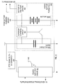
- a second solution to the above set of problems involves replacement of the second battery 322B in the dual battery power pack 320 of FIG. 3 with an alternative charge storage component in the form of a supercapacitor 422, thereby completing contents of a hybrid battery power pack 420 (see FIG. 4 ).
- a supercapacitor resembles a regular capacitor with the exception that a supercapacitor offers very high capacitance in a small package. Energy storage is accomplished by means of static charge rather than being accomplished by means of an electro-chemical process, such as in the manner of a conventional chemical battery.
- a supercapacitor In common with a regular capacitor, a supercapacitor has a positive plate and a negative plate. By applying a voltage differential to the positive and negative plates, a charge may be stored in the supercapacitor.
- a regular capacitor typically includes conductive foils and a dry separator
- the supercapacitor typically includes special electrodes and an electrolyte.
- the known Part No. EDLC152344-551-2F-30 by TDK of Nihombashi, Chuo, Tokyo, Japan is an example of a component that may be used for the supercapacitor 422. Specifications of this example component include: dimensions 23x44x1.5 mm; rated voltage ⁇ 4.2V continuous bias, 5.7V intermittent bias; and nominal capacitance 550mF.
- the concepts described herein are not limited, however, to any particular supercapacitor, or any particular capacitance, or any particular structure for charge storage or charge separation.
- the first battery 322A of hybrid battery power pack 420 has a first terminal connected to the battery charging circuit 126 and a second terminal connected to a common supply voltage for the power distribution network.
- a second terminal of the supercapacitor 422 is also connected to the common supply voltage for the power distribution network.
- a first terminal of the supercapacitor 422 and the first terminal of the first battery 322A are connected to, and interposed by, a supercapacitor charging circuit 421.
- the step-down DC-to-DC converter 128 converts the voltage available at the first terminal of the supercapacitor 422 to a lower voltage and makes the lower voltage available to the power amplifier circuit 124.
- the power distribution network 100 can be designed with more than one supercapacitor if there is more than one high current load.
- the hybrid battery power pack 420 includes a battery identifier and temperature sensor 426.
- the battery identifier and temperature sensor 426 connects to the processor 102 ( FIG. 1 ) to provide battery identity and information regarding the temperature of the hybrid battery power pack 420.
- the supercapacitor charging circuit 421 can act to maintain a consistent charge on the supercapacitor 422, thereby distinguishing the hybrid battery power pack 420 from a single-battery power pack, for which a consistent charge is desired but, as has been discussed hereinbefore, is difficult to achieve.
- the supercapacitor charging circuit 421, and the dual-battery charging circuit 321, may be implemented as a standard switched power supply, which can be a step-up converter or a step-down converter with a predetermined charging current.
- a standard switched power supply which can be a step-up converter or a step-down converter with a predetermined charging current.
- the present disclosure is not dependent on a particular implementation of charging circuit.
- the step-down DC-to-DC converter 128 may be short-circuited, so that the second battery 322B in the dual battery power pack 320 of FIG. 3 or the supercapacitor 422 in the hybrid battery power pack 420 of FIG. 4 is directly connected to the power amplifier circuit 124.
- the charging circuit e.g., the dual-battery charging circuit 321 in FIG. 3 or the supercapacitor charging circuit 421 in FIG. 4 , serves as both a charging circuit and a voltage regulating circuit.
- the second battery 322B or the supercapacitor 422 in these alternative embodiments retain their use as providers of the majority of the instant power required from the power amplifier circuit 124 during a pulsed high current draw.
- the charging circuit e.g., the dual-battery charging circuit 321 in FIG. 3 or the supercapacitor charging circuit 421 in FIG. 4
- the charging circuit may be short circuited, so that the second battery 322B or the supercapacitor 422 is directly connected to the first battery 322A, while the step-down DC-to-DC converter 128 is used to regulate the battery output voltage to a fixed supply voltage to the power amplifier circuit 124.
- the second battery 322B or the supercapacitor 422 in these alternative embodiments retain their use as providers of the majority of the instant power required from the power amplifier circuit 124 during a pulsed high current draw.
- the ESR of the combination of the step-down DC-to-DC converter 128 and the hybrid battery power pack 420 also has a lower ESR than a hypothetical single-battery power pack.
- the ESR of the hypothetical single-battery power pack may be in the order of 150 m ⁇ , while the ESR of the combination of the step-down DC-to-DC converter 128 and the hybrid battery power pack 420 may be in the order of only 30 m ⁇ .
- a third solution to the above set of problems involves rearrangement of the components of the hybrid battery power pack 420 of FIG. 4 such that only the first battery 322A remains inside a battery power pack, thereby leading to the naming of a solo battery power pack 520.
- the first battery 322A of a solo battery power pack 520 has a first terminal connected to the battery charging circuit 126 and a second terminal connected to a common supply voltage for the power distribution network.
- a first terminal of the supercapacitor 422 and the first terminal of the first battery 322A are connected to, and interposed by, the supercapacitor charging circuit 421.
- the step-down DC-to-DC converter 128 converts the voltage available at the first terminal of the supercapacitor 422 to a lower voltage and makes the lower voltage available to the power amplifier circuit 124.
- the solo battery power pack 520 includes a battery identifier and temperature sensor 526.
- the battery identifier and temperature sensor 526 connects to the processor 102 ( FIG. 1 ) to provide battery identity and information regarding the temperature of the solo battery power pack 520.
- the circuit of FIG. 5 includes additional components that may be found in mobile communication devices.
- the additional components include a Light Emitting Diode (LED) 532 for use as a flash when using the mobile communication device to capture a still photograph.
- the LED 532 may also be used as a torch to provide light when the mobile communication device is used to capture video.
- a controller 530 Associated with, and connected to, the LED 532 is a controller 530.
- the controller 530 receives power from the first terminal of the supercapacitor 422. Additionally, the controller 530 receives instructions from the processor 102 ( FIG. 1 ).
- the pulse mode of power amplifier operation is known to cause a ripple in the power supply voltage provided at a battery and that the ripple may be shown to adversely affect operation of other circuits. It may also be shown that other circuits in a typical mobile communication device can cause a ripple in the power supply voltage.
- An example of such a ripple-causing circuit is the combination of the LED 532 and the controller 530 in FIG. 5 .
- the power amplifier circuit 124 and the LED 532 may not be operated at the same time due to high pulsed power consumption and the resultant voltage ripples propagating to other circuits. It can be shown that use of the supercapacitor 422, with the step-down DC-to-DC converter 128 and the supercapacitor charging circuit 421, will allow simultaneous operation of the power amplifier circuit 124 and the LED 532, without causing significant power supply voltage ripples to propagate to other circuits. Indeed, testing has shown that power supply voltage ripples may be reduced from 400 mV peak-to-peak to less than 200 mV peak-to-peak.
- the circuit of FIG. 5 makes available continued operation of the mobile communication device even in the absence of the solo battery power pack 520. Accordingly, the mobile communication device may, for example, continue to participate in a cellular telephone call or continue to play a digital music file, even as a previously installed solo battery power pack is exchanged for a replacement solo battery power pack.
- efficiency of the power amplifier circuit 124 may be improved through designing the power amplifier circuit 124 for a tightly regulated supply voltage from the step-down DC-to-DC converter 128. Such improved efficiency during operation may be further improved by dynamically setting the output of the step-down DC-to-DC converter 128 to the power amplifier circuit 124 based on a desired output power level.
- the step-down DC-to-DC converter 128 may receive instructions from the processor 102 ( FIG. 1 ).
- the instructions may be of any kind, including instructions in the form of modulated pulses.
- the power amplifier 202 may be forced into a mode of operation known as "saturation".
- saturation the power level of the radio frequency (RF) signal output to the GSM/EDGE transceiver antenna 118E is reduced relative to a preferred power level in order to revert the power amplifier 202 out of the saturation.
- RF radio frequency
- the power amplifier current loop defined in FIG. 2 as being formed through the power pack 120 and the power amplifier 202 may be defined in FIGS. 4 and 5 as being formed through the step-down DC-to-DC converter 128, the supercapacitor 422 and the power amplifier 124.
- the relatively large area of the power amplifier current loop defined in FIG. 2 may be reduced by arranging the step-down DC-to-DC converter 128 and the supercapacitor 422 to be relatively closer to the power amplifier 124. Such an arrangement may be seen to be most feasible in the circuit of FIG. 5 , wherein the supercapacitor 422 is separate from the first battery 322A.
- RF interference signals have been discussed hereinbefore as being present at the power amplifier 202 ( FIG. 2 ) during transmission and being coupled to other circuits 104, 106, 108, 110, 112, 114, 116, 122, 126 via the power supply lines.
- the proposed power distribution network may be shown to reduce the decoupling requirements for all mobile sub circuits.
- Relatively long power supply traces on a printed circuit board (PCB) used to implement power distribution networks are known to occupy PCB real estate and maintain a relatively high ESR, which may be considered detrimental to the efficiency of power supplied by the power pack.
- a further consequence of the proposed reduced-area power amplifier current loop defined in FIG. 5 is a reduction in length of power supply traces, thereby preserving PCB real estate and reducing the ESR of the power supply traces, leading to an increase in the efficiency of the use of the power from the first battery 322A.
- the alternative charge storage component need not be restricted to the supercapacitor 422 of FIGS. 4 and 5 . Indeed, many other types of capacitors may be suitable.
- a charging circuit is described as circuitry that can deliver electrical power from a power supply (which may include one or more charge storage components) to a component that consumes the electrical power.
- a power supply which may include one or more charge storage components
- the charging circuits and converters have been illustrated as distinct elements. In practice, however, charging circuits and converters may be combined and may share some circuit elements.
- converters for use as the converter 128, including switched converters.
- the converter 128 has been disclosed as a step-down DC-to-DC converter, there exist applications in which a step-up converter would be more appropriate.
- the power amplifier circuit 124 may be designed to use a supply voltage that is higher than the voltage available from the installed power pack.
- converters that only step-up or step-down there exist converters that both step-up and step-down.
- the above-described embodiments, and variations thereof, may realize one or more advantages, some of which have been previously mentioned.
- the circuit supplying power to the power amplifier 202 FIG. 2
- vendors will have more freedom and flexibility to design the power amplifier circuit 124 and, more specifically, the power amplifier 202.
- the dual-battery charging circuit 321 FIG. 3
- the ESR of the second battery 322B may be maintained at a magnitude that is consistently lower than the ESR of the first battery 322A so that a majority of the high pulsed current drawn by the power amplifier circuit 124 will pass though the second battery 322B. Further advantageously, the circuit of FIG. 5 makes available continued operation of the mobile communication device even in the absence of the solo battery power pack 520.
Landscapes
- Engineering & Computer Science (AREA)
- Power Engineering (AREA)
- Charge And Discharge Circuits For Batteries Or The Like (AREA)
- Battery Mounting, Suspending (AREA)
Claims (12)
- Réseau de distribution de puissance comprenant :un circuit de charge primaire ;un premier composant de stockage de charge ayant une première borne reliée audit circuit de charge primaire et une deuxième borne reliée à une tension commune d'alimentation électrique ;un circuit de charge secondaire relié à ladite première borne dudit premier composant de stockage de charge ;un deuxième composant de stockage de charge ayant une première borne reliée audit circuit de charge secondaire et une deuxième borne reliée à ladite tension commune d'alimentation électrique ;un convertisseur ayant une borne d'entrée et une borne de sortie, ladite borne d'entrée recevant une tension d'entrée provenant de ladite première borne dudit deuxième composant de stockage de charge et ladite borne de sortie fournissant une tension de sortie avec une amplitude modifiée par rapport à ladite tension d'entrée ; etun circuit amplificateur de puissance relié à ladite borne de sortie dudit convertisseur pour recevoir ladite tension de sortie, caractérisé en ce que ledit circuit amplificateur de puissance étant conçu selon une plage de variation de ladite tension de sortie.
- Réseau de distribution de puissance de la revendication 1, dans lequel ledit premier composant de stockage de charge comprend une batterie.
- Réseau de distribution de puissance de la revendication 1 ou 2, dans lequel ledit deuxième composant de stockage de charge comprend une batterie.
- Réseau de distribution de puissance de la revendication 1 ou 2, dans lequel ledit deuxième composant de stockage de charge comprend un supercondensateur.
- Réseau de distribution de puissance de l'une quelconque des revendications 1 à 4, comprenant en outre un bloc d'alimentation renfermant ledit premier composant de stockage de charge, ledit circuit de charge secondaire et ledit deuxième composant de stockage de charge.
- Réseau de distribution de puissance de la revendication 5, comprenant en outre un identificateur de batterie enfermé par ledit bloc d'alimentation et relié à ladite première borne dudit premier composant de stockage.
- Réseau de distribution de puissance de la revendication 6, dans lequel ledit identificateur de batterie est adapté pour délivrer en sortie une identification dudit bloc d'alimentation.
- Réseau de distribution de puissance de l'une quelconque des revendications 5 à 7, comprenant en outre un capteur de température enfermé par ledit bloc d'alimentation et adapté pour détecter une température à l'intérieur dudit bloc d'alimentation et pour fournir un signal de sortie qui indique ladite température.
- Réseau de distribution de puissance de l'une quelconque des revendications 1 à 4, comprenant en outre un bloc d'alimentation renfermant ledit premier composant de stockage de charge.
- Réseau de distribution de puissance de la revendication 9, comprenant en outre un identificateur de batterie enfermé par ledit bloc d'alimentation et relié à ladite première borne dudit premier composant de stockage.
- Réseau de distribution de puissance de la revendication 10, dans lequel ledit identificateur de batterie est adapté pour délivrer en sortie une identification dudit bloc d'alimentation.
- Réseau de distribution de puissance de l'une quelconque des revendications 9 à 11, comprenant en outre un capteur de température enfermé par ledit bloc d'alimentation et adapté pour détecter une température à l'intérieur dudit bloc d'alimentation et pour fournir un signal de sortie qui indique ladite température.
Priority Applications (4)
| Application Number | Priority Date | Filing Date | Title |
|---|---|---|---|
| EP10153698.5A EP2360809B1 (fr) | 2010-02-16 | 2010-02-16 | Réseau de distribution d'énergie basé sur des composants de stockage à charge multiple |
| CN2011100395271A CN102163879A (zh) | 2010-02-16 | 2011-02-15 | 基于多个电荷存储组件的功率分配网络 |
| CA2731894A CA2731894C (fr) | 2010-02-16 | 2011-02-16 | Reseau de distributtion d'energie base sur de multiples composants de stockage de charges |
| HK11109463.6A HK1155283B (en) | 2011-09-07 | Power distribution network based on multiple charge storage components |
Applications Claiming Priority (1)
| Application Number | Priority Date | Filing Date | Title |
|---|---|---|---|
| EP10153698.5A EP2360809B1 (fr) | 2010-02-16 | 2010-02-16 | Réseau de distribution d'énergie basé sur des composants de stockage à charge multiple |
Publications (2)
| Publication Number | Publication Date |
|---|---|
| EP2360809A1 EP2360809A1 (fr) | 2011-08-24 |
| EP2360809B1 true EP2360809B1 (fr) | 2015-04-08 |
Family
ID=42272289
Family Applications (1)
| Application Number | Title | Priority Date | Filing Date |
|---|---|---|---|
| EP10153698.5A Active EP2360809B1 (fr) | 2010-02-16 | 2010-02-16 | Réseau de distribution d'énergie basé sur des composants de stockage à charge multiple |
Country Status (3)
| Country | Link |
|---|---|
| EP (1) | EP2360809B1 (fr) |
| CN (1) | CN102163879A (fr) |
| CA (1) | CA2731894C (fr) |
Families Citing this family (7)
| Publication number | Priority date | Publication date | Assignee | Title |
|---|---|---|---|---|
| US8810209B2 (en) | 2011-12-22 | 2014-08-19 | Blackberry Limited | Power distribution network based on multiple charge storage components |
| EP2608353B1 (fr) * | 2011-12-22 | 2016-03-09 | BlackBerry Limited | Réseau de distribution d'énergie basé sur des composants de stockage à charge multiple |
| KR101539689B1 (ko) * | 2012-02-20 | 2015-07-27 | 주식회사 엘지화학 | 멀티 bms에 대한 식별자 할당 시스템 및 방법 |
| US8896374B2 (en) * | 2012-07-25 | 2014-11-25 | Qualcomm Incorporated | Energy source sharing |
| CN106451509B (zh) * | 2016-10-20 | 2019-01-15 | 山西大学 | 基于复合储能的能量管控优化方法 |
| GB2565006B (en) * | 2018-11-09 | 2021-09-08 | O2Micro International Ltd | Battery protection systems |
| CN121238976B (zh) * | 2025-12-02 | 2026-02-27 | 西安中甲电气有限责任公司 | 基于云边协同的低纹波高压电源比优化管理方法 |
Family Cites Families (5)
| Publication number | Priority date | Publication date | Assignee | Title |
|---|---|---|---|---|
| US5587250A (en) * | 1995-09-27 | 1996-12-24 | Motorola, Inc. | Hybrid energy storage system |
| US6215274B1 (en) * | 1999-10-27 | 2001-04-10 | Denso Corporation | Enhanced battery pack monitoring interface |
| AUPQ750400A0 (en) * | 2000-05-15 | 2000-06-08 | Energy Storage Systems Pty Ltd | A power supply |
| JP2004297753A (ja) * | 2003-02-07 | 2004-10-21 | Nec Tokin Corp | 電源回路、及び該電源回路を備えた通信機器 |
| EP2083511B1 (fr) * | 2008-01-25 | 2014-01-22 | Actaris SAS | Alimentation à pile pour èmetteur radiofréquences |
-
2010
- 2010-02-16 EP EP10153698.5A patent/EP2360809B1/fr active Active
-
2011
- 2011-02-15 CN CN2011100395271A patent/CN102163879A/zh active Pending
- 2011-02-16 CA CA2731894A patent/CA2731894C/fr active Active
Also Published As
| Publication number | Publication date |
|---|---|
| CA2731894A1 (fr) | 2011-08-16 |
| CA2731894C (fr) | 2015-02-03 |
| EP2360809A1 (fr) | 2011-08-24 |
| CN102163879A (zh) | 2011-08-24 |
| HK1155283A1 (en) | 2012-05-11 |
Similar Documents
| Publication | Publication Date | Title |
|---|---|---|
| EP2360809B1 (fr) | Réseau de distribution d'énergie basé sur des composants de stockage à charge multiple | |
| US8760125B2 (en) | Power distribution network based on multiple charge storage components | |
| US20250125644A1 (en) | Adaptive power systems and techniques | |
| US8810209B2 (en) | Power distribution network based on multiple charge storage components | |
| EP4068605A1 (fr) | Terminal, son procédé d'alimentation électrique, et circuit de gestion de charge et de décharge | |
| US9882403B2 (en) | Battery module | |
| US8483778B2 (en) | Mobile communication device employing power pack with multiple pairs of taps | |
| EP3934053B1 (fr) | Dispositif d'alimentation électrique, appareil électronique et procédé d'alimentation électrique | |
| EP3905476A1 (fr) | Dispositif et procédé d'alimentation électrique, et dispositif électronique | |
| CN101884151A (zh) | 便携式无线电装置及电池组配置 | |
| CN101120618A (zh) | 电源 | |
| CA2799837C (fr) | Reseau de distribution d'energie base sur de multiples composants de stockage de charge | |
| EP2360808B1 (fr) | Dispositif de communication mobile utilisant un bloc d'alimentation avec plusieurs paires de prises | |
| KR20200099057A (ko) | 복수의 셀이 직렬 연결된 배터리에 사용가능한 전력관리장치 | |
| HK1155283B (en) | Power distribution network based on multiple charge storage components | |
| CN113859552B (zh) | 一种电池管理系统 | |
| US20220302734A1 (en) | Parallel charger circuit with battery feedback control | |
| HK1155282B (en) | Mobile communication device employing power pack with multiple pairs of taps | |
| KR20260047063A (ko) | 외부의 전력 공급 장치로부터 유선으로 전력을 수신하고 외부의 전력 수신 장치로 무선으로 전력을 공급하는 전자 장치 |
Legal Events
| Date | Code | Title | Description |
|---|---|---|---|
| PUAI | Public reference made under article 153(3) epc to a published international application that has entered the european phase |
Free format text: ORIGINAL CODE: 0009012 |
|
| 17P | Request for examination filed |
Effective date: 20100216 |
|
| AK | Designated contracting states |
Kind code of ref document: A1 Designated state(s): AT BE BG CH CY CZ DE DK EE ES FI FR GB GR HR HU IE IS IT LI LT LU LV MC MK MT NL NO PL PT RO SE SI SK SM TR |
|
| AX | Request for extension of the european patent |
Extension state: AL BA RS |
|
| REG | Reference to a national code |
Ref country code: HK Ref legal event code: DE Ref document number: 1155283 Country of ref document: HK |
|
| RAP1 | Party data changed (applicant data changed or rights of an application transferred) |
Owner name: BLACKBERRY LIMITED |
|
| RAP1 | Party data changed (applicant data changed or rights of an application transferred) |
Owner name: BLACKBERRY LIMITED |
|
| GRAP | Despatch of communication of intention to grant a patent |
Free format text: ORIGINAL CODE: EPIDOSNIGR1 |
|
| INTG | Intention to grant announced |
Effective date: 20141023 |
|
| GRAS | Grant fee paid |
Free format text: ORIGINAL CODE: EPIDOSNIGR3 |
|
| GRAA | (expected) grant |
Free format text: ORIGINAL CODE: 0009210 |
|
| AK | Designated contracting states |
Kind code of ref document: B1 Designated state(s): AT BE BG CH CY CZ DE DK EE ES FI FR GB GR HR HU IE IS IT LI LT LU LV MC MK MT NL NO PL PT RO SE SI SK SM TR |
|
| REG | Reference to a national code |
Ref country code: GB Ref legal event code: FG4D |
|
| REG | Reference to a national code |
Ref country code: CH Ref legal event code: EP |
|
| REG | Reference to a national code |
Ref country code: IE Ref legal event code: FG4D |
|
| REG | Reference to a national code |
Ref country code: AT Ref legal event code: REF Ref document number: 721204 Country of ref document: AT Kind code of ref document: T Effective date: 20150515 |
|
| REG | Reference to a national code |
Ref country code: DE Ref legal event code: R096 Ref document number: 602010023709 Country of ref document: DE Effective date: 20150521 |
|
| REG | Reference to a national code |
Ref country code: NL Ref legal event code: T3 |
|
| REG | Reference to a national code |
Ref country code: NL Ref legal event code: T3 |
|
| REG | Reference to a national code |
Ref country code: AT Ref legal event code: MK05 Ref document number: 721204 Country of ref document: AT Kind code of ref document: T Effective date: 20150408 |
|
| REG | Reference to a national code |
Ref country code: LT Ref legal event code: MG4D |
|
| PG25 | Lapsed in a contracting state [announced via postgrant information from national office to epo] |
Ref country code: FI Free format text: LAPSE BECAUSE OF FAILURE TO SUBMIT A TRANSLATION OF THE DESCRIPTION OR TO PAY THE FEE WITHIN THE PRESCRIBED TIME-LIMIT Effective date: 20150408 Ref country code: HR Free format text: LAPSE BECAUSE OF FAILURE TO SUBMIT A TRANSLATION OF THE DESCRIPTION OR TO PAY THE FEE WITHIN THE PRESCRIBED TIME-LIMIT Effective date: 20150408 Ref country code: LT Free format text: LAPSE BECAUSE OF FAILURE TO SUBMIT A TRANSLATION OF THE DESCRIPTION OR TO PAY THE FEE WITHIN THE PRESCRIBED TIME-LIMIT Effective date: 20150408 Ref country code: NO Free format text: LAPSE BECAUSE OF FAILURE TO SUBMIT A TRANSLATION OF THE DESCRIPTION OR TO PAY THE FEE WITHIN THE PRESCRIBED TIME-LIMIT Effective date: 20150708 Ref country code: ES Free format text: LAPSE BECAUSE OF FAILURE TO SUBMIT A TRANSLATION OF THE DESCRIPTION OR TO PAY THE FEE WITHIN THE PRESCRIBED TIME-LIMIT Effective date: 20150408 Ref country code: PT Free format text: LAPSE BECAUSE OF FAILURE TO SUBMIT A TRANSLATION OF THE DESCRIPTION OR TO PAY THE FEE WITHIN THE PRESCRIBED TIME-LIMIT Effective date: 20150810 |
|
| PG25 | Lapsed in a contracting state [announced via postgrant information from national office to epo] |
Ref country code: LV Free format text: LAPSE BECAUSE OF FAILURE TO SUBMIT A TRANSLATION OF THE DESCRIPTION OR TO PAY THE FEE WITHIN THE PRESCRIBED TIME-LIMIT Effective date: 20150408 Ref country code: AT Free format text: LAPSE BECAUSE OF FAILURE TO SUBMIT A TRANSLATION OF THE DESCRIPTION OR TO PAY THE FEE WITHIN THE PRESCRIBED TIME-LIMIT Effective date: 20150408 Ref country code: GR Free format text: LAPSE BECAUSE OF FAILURE TO SUBMIT A TRANSLATION OF THE DESCRIPTION OR TO PAY THE FEE WITHIN THE PRESCRIBED TIME-LIMIT Effective date: 20150709 Ref country code: IS Free format text: LAPSE BECAUSE OF FAILURE TO SUBMIT A TRANSLATION OF THE DESCRIPTION OR TO PAY THE FEE WITHIN THE PRESCRIBED TIME-LIMIT Effective date: 20150808 |
|
| REG | Reference to a national code |
Ref country code: DE Ref legal event code: R097 Ref document number: 602010023709 Country of ref document: DE |
|
| REG | Reference to a national code |
Ref country code: HK Ref legal event code: GR Ref document number: 1155283 Country of ref document: HK |
|
| PG25 | Lapsed in a contracting state [announced via postgrant information from national office to epo] |
Ref country code: DK Free format text: LAPSE BECAUSE OF FAILURE TO SUBMIT A TRANSLATION OF THE DESCRIPTION OR TO PAY THE FEE WITHIN THE PRESCRIBED TIME-LIMIT Effective date: 20150408 Ref country code: EE Free format text: LAPSE BECAUSE OF FAILURE TO SUBMIT A TRANSLATION OF THE DESCRIPTION OR TO PAY THE FEE WITHIN THE PRESCRIBED TIME-LIMIT Effective date: 20150408 |
|
| PLBE | No opposition filed within time limit |
Free format text: ORIGINAL CODE: 0009261 |
|
| STAA | Information on the status of an ep patent application or granted ep patent |
Free format text: STATUS: NO OPPOSITION FILED WITHIN TIME LIMIT |
|
| REG | Reference to a national code |
Ref country code: FR Ref legal event code: PLFP Year of fee payment: 7 |
|
| PG25 | Lapsed in a contracting state [announced via postgrant information from national office to epo] |
Ref country code: SK Free format text: LAPSE BECAUSE OF FAILURE TO SUBMIT A TRANSLATION OF THE DESCRIPTION OR TO PAY THE FEE WITHIN THE PRESCRIBED TIME-LIMIT Effective date: 20150408 Ref country code: PL Free format text: LAPSE BECAUSE OF FAILURE TO SUBMIT A TRANSLATION OF THE DESCRIPTION OR TO PAY THE FEE WITHIN THE PRESCRIBED TIME-LIMIT Effective date: 20150408 Ref country code: RO Free format text: LAPSE BECAUSE OF NON-PAYMENT OF DUE FEES Effective date: 20150408 Ref country code: CZ Free format text: LAPSE BECAUSE OF FAILURE TO SUBMIT A TRANSLATION OF THE DESCRIPTION OR TO PAY THE FEE WITHIN THE PRESCRIBED TIME-LIMIT Effective date: 20150408 |
|
| 26N | No opposition filed |
Effective date: 20160111 |
|
| PG25 | Lapsed in a contracting state [announced via postgrant information from national office to epo] |
Ref country code: IT Free format text: LAPSE BECAUSE OF FAILURE TO SUBMIT A TRANSLATION OF THE DESCRIPTION OR TO PAY THE FEE WITHIN THE PRESCRIBED TIME-LIMIT Effective date: 20150408 |
|
| PG25 | Lapsed in a contracting state [announced via postgrant information from national office to epo] |
Ref country code: SI Free format text: LAPSE BECAUSE OF FAILURE TO SUBMIT A TRANSLATION OF THE DESCRIPTION OR TO PAY THE FEE WITHIN THE PRESCRIBED TIME-LIMIT Effective date: 20150408 Ref country code: BE Free format text: LAPSE BECAUSE OF NON-PAYMENT OF DUE FEES Effective date: 20160229 |
|
| PG25 | Lapsed in a contracting state [announced via postgrant information from national office to epo] |
Ref country code: BE Free format text: LAPSE BECAUSE OF FAILURE TO SUBMIT A TRANSLATION OF THE DESCRIPTION OR TO PAY THE FEE WITHIN THE PRESCRIBED TIME-LIMIT Effective date: 20150408 |
|
| PG25 | Lapsed in a contracting state [announced via postgrant information from national office to epo] |
Ref country code: LU Free format text: LAPSE BECAUSE OF FAILURE TO SUBMIT A TRANSLATION OF THE DESCRIPTION OR TO PAY THE FEE WITHIN THE PRESCRIBED TIME-LIMIT Effective date: 20160216 Ref country code: MC Free format text: LAPSE BECAUSE OF FAILURE TO SUBMIT A TRANSLATION OF THE DESCRIPTION OR TO PAY THE FEE WITHIN THE PRESCRIBED TIME-LIMIT Effective date: 20150408 |
|
| REG | Reference to a national code |
Ref country code: CH Ref legal event code: PL |
|
| PG25 | Lapsed in a contracting state [announced via postgrant information from national office to epo] |
Ref country code: CH Free format text: LAPSE BECAUSE OF NON-PAYMENT OF DUE FEES Effective date: 20160229 Ref country code: LI Free format text: LAPSE BECAUSE OF NON-PAYMENT OF DUE FEES Effective date: 20160229 |
|
| REG | Reference to a national code |
Ref country code: IE Ref legal event code: MM4A |
|
| PG25 | Lapsed in a contracting state [announced via postgrant information from national office to epo] |
Ref country code: IE Free format text: LAPSE BECAUSE OF NON-PAYMENT OF DUE FEES Effective date: 20160216 |
|
| REG | Reference to a national code |
Ref country code: FR Ref legal event code: PLFP Year of fee payment: 8 |
|
| PG25 | Lapsed in a contracting state [announced via postgrant information from national office to epo] |
Ref country code: SE Free format text: LAPSE BECAUSE OF FAILURE TO SUBMIT A TRANSLATION OF THE DESCRIPTION OR TO PAY THE FEE WITHIN THE PRESCRIBED TIME-LIMIT Effective date: 20150408 |
|
| PG25 | Lapsed in a contracting state [announced via postgrant information from national office to epo] |
Ref country code: MT Free format text: LAPSE BECAUSE OF FAILURE TO SUBMIT A TRANSLATION OF THE DESCRIPTION OR TO PAY THE FEE WITHIN THE PRESCRIBED TIME-LIMIT Effective date: 20150408 |
|
| REG | Reference to a national code |
Ref country code: FR Ref legal event code: PLFP Year of fee payment: 9 |
|
| PG25 | Lapsed in a contracting state [announced via postgrant information from national office to epo] |
Ref country code: HU Free format text: LAPSE BECAUSE OF FAILURE TO SUBMIT A TRANSLATION OF THE DESCRIPTION OR TO PAY THE FEE WITHIN THE PRESCRIBED TIME-LIMIT; INVALID AB INITIO Effective date: 20100216 Ref country code: SM Free format text: LAPSE BECAUSE OF FAILURE TO SUBMIT A TRANSLATION OF THE DESCRIPTION OR TO PAY THE FEE WITHIN THE PRESCRIBED TIME-LIMIT Effective date: 20150408 Ref country code: CY Free format text: LAPSE BECAUSE OF FAILURE TO SUBMIT A TRANSLATION OF THE DESCRIPTION OR TO PAY THE FEE WITHIN THE PRESCRIBED TIME-LIMIT Effective date: 20150408 |
|
| PG25 | Lapsed in a contracting state [announced via postgrant information from national office to epo] |
Ref country code: MT Free format text: LAPSE BECAUSE OF FAILURE TO SUBMIT A TRANSLATION OF THE DESCRIPTION OR TO PAY THE FEE WITHIN THE PRESCRIBED TIME-LIMIT Effective date: 20160229 Ref country code: TR Free format text: LAPSE BECAUSE OF FAILURE TO SUBMIT A TRANSLATION OF THE DESCRIPTION OR TO PAY THE FEE WITHIN THE PRESCRIBED TIME-LIMIT Effective date: 20150408 Ref country code: MK Free format text: LAPSE BECAUSE OF FAILURE TO SUBMIT A TRANSLATION OF THE DESCRIPTION OR TO PAY THE FEE WITHIN THE PRESCRIBED TIME-LIMIT Effective date: 20150408 |
|
| PG25 | Lapsed in a contracting state [announced via postgrant information from national office to epo] |
Ref country code: BG Free format text: LAPSE BECAUSE OF FAILURE TO SUBMIT A TRANSLATION OF THE DESCRIPTION OR TO PAY THE FEE WITHIN THE PRESCRIBED TIME-LIMIT Effective date: 20150408 |
|
| REG | Reference to a national code |
Ref country code: DE Ref legal event code: R082 Ref document number: 602010023709 Country of ref document: DE Ref country code: DE Ref legal event code: R081 Ref document number: 602010023709 Country of ref document: DE Owner name: MALIKIE INNOVATIONS LTD., IE Free format text: FORMER OWNER: BLACKBERRY LTD., WATERLOO, ONTARIO, CA |
|
| PGFP | Annual fee paid to national office [announced via postgrant information from national office to epo] |
Ref country code: NL Payment date: 20260220 Year of fee payment: 17 |
|
| PGFP | Annual fee paid to national office [announced via postgrant information from national office to epo] |
Ref country code: GB Payment date: 20260223 Year of fee payment: 17 |
|
| PGFP | Annual fee paid to national office [announced via postgrant information from national office to epo] |
Ref country code: DE Payment date: 20260220 Year of fee payment: 17 |
|
| PGFP | Annual fee paid to national office [announced via postgrant information from national office to epo] |
Ref country code: FR Payment date: 20260224 Year of fee payment: 17 |