EP2360910A2 - Bilderfassungsvorrichtung - Google Patents
Bilderfassungsvorrichtung Download PDFInfo
- Publication number
- EP2360910A2 EP2360910A2 EP11150254A EP11150254A EP2360910A2 EP 2360910 A2 EP2360910 A2 EP 2360910A2 EP 11150254 A EP11150254 A EP 11150254A EP 11150254 A EP11150254 A EP 11150254A EP 2360910 A2 EP2360910 A2 EP 2360910A2
- Authority
- EP
- European Patent Office
- Prior art keywords
- flicker
- image
- image sensor
- flicker detection
- unit
- Prior art date
- Legal status (The legal status is an assumption and is not a legal conclusion. Google has not performed a legal analysis and makes no representation as to the accuracy of the status listed.)
- Granted
Links
Images


Classifications
-
- H—ELECTRICITY
- H04—ELECTRIC COMMUNICATION TECHNIQUE
- H04N—PICTORIAL COMMUNICATION, e.g. TELEVISION
- H04N23/00—Cameras or camera modules comprising electronic image sensors; Control thereof
- H04N23/70—Circuitry for compensating brightness variation in the scene
-
- H—ELECTRICITY
- H04—ELECTRIC COMMUNICATION TECHNIQUE
- H04N—PICTORIAL COMMUNICATION, e.g. TELEVISION
- H04N23/00—Cameras or camera modules comprising electronic image sensors; Control thereof
- H04N23/60—Control of cameras or camera modules
- H04N23/69—Control of means for changing angle of the field of view, e.g. optical zoom objectives or electronic zooming
-
- H—ELECTRICITY
- H04—ELECTRIC COMMUNICATION TECHNIQUE
- H04N—PICTORIAL COMMUNICATION, e.g. TELEVISION
- H04N23/00—Cameras or camera modules comprising electronic image sensors; Control thereof
- H04N23/70—Circuitry for compensating brightness variation in the scene
- H04N23/745—Detection of flicker frequency or suppression of flicker wherein the flicker is caused by illumination, e.g. due to fluorescent tube illumination or pulsed LED illumination
-
- H—ELECTRICITY
- H04—ELECTRIC COMMUNICATION TECHNIQUE
- H04N—PICTORIAL COMMUNICATION, e.g. TELEVISION
- H04N23/00—Cameras or camera modules comprising electronic image sensors; Control thereof
- H04N23/70—Circuitry for compensating brightness variation in the scene
- H04N23/73—Circuitry for compensating brightness variation in the scene by influencing the exposure time
Definitions
- the present invention relates to an image capture apparatus and, more particularly, to an image capture apparatus for capturing a moving image.
- the brightness may vary for each frame or light/dark horizontal stripes may be generated in a frame due to blinking of the fluorescent light at the frequency of the commercial power supply.
- This light/dark variation is called a flicker.
- the flicker can be reduced by controlling the electronic shutter to a shutter speed of n/100 seconds (n is a natural number) for a 50-Hz flicker and n/120 s for a 60-Hz flicker.
- n/100 seconds n is a natural number
- n/120 s for a 60-Hz flicker.
- Japanese Patent Laid-Open No. 2007-60585 discloses a method of integrating video signals obtained from a CMOS sensor for one or more horizontal periods and comparing the integration values of preceding and succeeding frames to detect a flicker.
- Some image capture apparatuses which have an image sensor capable of reading out a specific region, have a function of reading out a region smaller than the entire region of the image sensor, thereby performing zooming or zooming in (i.e. magnifying) without using a zoom lens.
- Japanese Patent Laid-Open No. 2002-314868 discloses a method of performing high-resolution zooming by changing the readout range and driving method of the image sensor.
- the problem of flicker also arises when zooming is performed in this way, namely by reading out a specific region that is a sub-region of the maximum input object image receivable by the image sensor.
- the flicker can be detected using the above-described method of comparing the integration values of preceding and succeeding frames.
- the present invention provides an image capture apparatus as specified in claims 1 to 3.
- a second aspect of the present invention is defined according to method claims 4 to 6.
- Fig. 1 is a block diagram showing the arrangement of an image capture apparatus according to an embodiment of the present invention
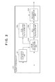
- Fig. 2 is a block diagram showing the arrangement of the flicker detection unit of the image capture apparatus according to the embodiment
- Figs. 3A and 3B are graphs showing the outputs of a line integration unit and a frame difference calculation unit according to the embodiment.
- Fig. 4 is a flowchart illustrating the operation of the system control unit of the image capture apparatus according to the embodiment.
- Fig. 1 is a block diagram showing the arrangement of an image capture apparatus according to an embodiment of the present invention.
- An image capture apparatus 100 according to the embodiment of the present invention will be described with reference to Fig. 1 .
- a light beam that has entered an imaging lens 111 forms an optical image on an image sensor 113 via a stop 112.
- the stop 112 is driven based on a signal output from a stop driving unit 142.
- the stop driving unit 142 outputs a stop driving amount to the stop 112 under the control of a device control unit 133 in a system control unit 131.
- the image sensor 113 is, for example, an X-Y address scan type CMOS sensor which is driven based on a timing signal output from a timing generator 143 so as to photoelectrically convert an object image into an analog electric signal.
- the timing generator 143 outputs the timing signal for controlling the electronic shutter to the image sensor 113 upon receiving an instruction from the device control unit 133.
- the timing generator 143 also outputs, to the image sensor 113, a readout start position and end position designated by the device control unit 133.
- the image capture apparatus of this embodiment has a first driving method and a second driving method.
- the first driving method reads out pixel signals in almost the entire region (maximum angle of view) of the image sensor 113.
- the second driving method reads out pixel signals in a region of an angle of view narrower than in the first driving method. That is, an image read out by the second driving method is a zoomed-in (or magnified) image.
- Multilevel zooming may be enabled by providing a plurality of driving methods including, for example, a third driving method of reading out an angle of view narrower than in the second driving method and a fourth driving method of reading out an angle of view narrower than in the third driving method.
- a plurality or range of zoom or magnifying levels are possible.
- angle of view of readout need only satisfy the following inequality: angle of view by first driving method > angle of view by second driving method . That is, in any driving method, if the relation of the angles of view is maintained, the readout data amount can be reduced by performing readout while adding several pixels or skipping every few pixels.
- An analog signal processing unit 114 samples and holds the analog signal from the image sensor 113, adds an analog gain, A/D-converts the analog signal into a digital signal, and outputs it.
- the analog gain addition amount is based on the input from the device control unit 133.
- a digital signal processing unit 121 performs digital signal processing of the digital signal output from the analog signal processing unit 114, and stores it in a memory 152 via a memory control unit 151.
- the digital signal processing unit 121 also reads out, via the memory control unit 151, the digital video signal stored in the memory 152, and outputs it to an image display unit 161.
- the digital signal processing unit 121 includes a digital gain unit 122, image processing unit 123, photometric value calculation unit 124, line integration unit 125, and display control unit 126.
- the digital gain unit 122 adds a digital gain to the digital signal, and outputs it to the image processing unit 123, photometric value calculation unit 124, and line integration unit 125.
- the device control unit 133 designates the digital gain amount.
- the image processing unit 123 executes various kinds of digital signal processing such as pixel interpolation processing, color conversion processing, and resolution conversion processing.
- the photometric value calculation unit 124 calculates a photometric value by integrating digital signals output from the digital gain unit 122, and transmits the photometric value to an exposure control unit 132.
- the line integration unit 125 integrates image signals input from the digital gain unit in the horizontal direction, and outputs the integration result to a flicker detection unit 135.
- the display control unit 126 stores the output from the image processing unit 123 in the memory 152 via the memory control unit 151.
- the display control unit 126 also reads out, via the memory control unit 151, the digital video signal stored in the memory 152, and outputs it to the image display unit 161.
- the display control unit 126 also switches the display on the image display unit 161 upon receiving a video signal display/non-display instruction from the system control unit 131.
- the image display unit 161 is an image display device such as a liquid crystal display (LCD) and displays, for example, a moving image that is being captured or image capture information set by the user.
- An operation unit 141 includes an operation button to be used to set the zooming ratio of a captured image, and outputs a user input operation to the system control unit 131.
- the operation unit 141 also includes a moving image recording start instruction button, exposure correction value change operation dial, and various kinds of operation buttons.
- the system control unit 131 is a microcomputer including a CPU, ROM, and RAM, and executes programs stored in the ROM.
- the system control unit 131 includes the exposure control unit 132, device control unit 133, readout region instruction unit 134, and flicker detection unit 135 which detects the flicker of a light source that illuminates an object.
- the exposure control unit 132 determines the stop driving amount, shutter speed, analog gain amount, and digital gain amount based on the photometric value output from the photometric value calculation unit 124. If the flicker detection unit 135 indicates that flicker detection is progressing, the exposure control unit 132 does not select the shutter speed for reducing the flicker. That is, a shutter speed corresponding to neither n/100 s (where n is a natural number) nor n/120 s is output. When the flicker detection unit 135 detects a 50-Hz flicker, the exposure control unit 132 preferentially selects a shutter speed of n/100 s. Upon detecting a 60-Hz flicker, the exposure control unit 132 preferentially selects a shutter speed of n/120 s.
- the readout region instruction unit 134 determines the zooming ratio of a captured image in accordance with the operation on the operation unit 141. If the flicker detection unit 135 indicates that flicker detection is progressing, the readout region instruction unit 134 designates an unzooming state, that is, the region of the image sensor 113 for the first reading method. When flicker detection of the flicker detection unit 135 has ended, the readout region instruction unit 134 determines the readout region of the image sensor 113 based on the zooming ratio preset by the operation on the operation unit 141, and outputs it to the device control unit 133.
- the device control unit 133 Based on the input from the exposure control unit 132, the device control unit 133 outputs an electronic shutter control value to the timing generator 143, a stop driving amount to the stop driving unit 142, and gain amounts to the analog signal processing unit 114 and the digital gain unit 122.
- the device control unit 133 also designates the readout region of the image sensor 113 and the operation frame rate for the timing generator 143 based on the input from the readout region instruction unit 134.
- the flicker detection unit 135 analyzes the digital signal, extracts the flicker component in the signal, determines the presence/absence of a flicker and the flicker frequency, and outputs the determination result.
- Fig. 2 is a block diagram showing the arrangement of the flicker detection unit 135.
- the flicker detection unit 135 includes an integration value delay unit 301, frame difference calculation unit 302, 50-Hz autocorrelation calculation unit 303, 60-Hz autocorrelation calculation unit 304, and frequency determination unit 305.
- the integration value delay unit 301 holds the integration value of an immediately preceding frame input from the line integration unit 125, and outputs the integration value of the immediately preceding frame to the frame difference calculation unit 302.
- Fig. 3A shows the output waveform of the line integration unit 125 when the captured object has a uniform brightness surface.
- N frame indicates the output waveform of the line integration unit 125
- (N-1) frame indicates the output waveform of the integration value delay unit 301.
- the frame difference calculation unit 302 calculates the difference between the integration value from the line integration unit 125 and that from the integration value delay unit 301, thereby removing the reflectance component of the object and extracting only the flicker component.
- Fig. 3B shows an example of the output waveform of the frame difference calculation unit 302.
- the 50-Hz autocorrelation calculation unit 303 and the 60-Hz autocorrelation calculation unit 304 auto-correlate the flicker component input from the frame difference calculation unit 302, and output a 50-Hz flicker correlation value R 50Hz , and a 60-Hz flicker correlation value R 60Hz to the frequency determination unit 305, respectively.
- y0 is an arbitrary line position
- 1 is the integration value acquisition section.
- the frequency determination unit 305 has thresholds Th 50Hz and Th 60Hz for the flicker evaluation values, and makes determination in the following way.
- the flicker frequency can be specified if a captured image corresponding to two frames exists. Repeating the above-described processing enables the increase of the reliability of flicker frequency determination. For example, if one of the results (1) to (4) is obtained continuously three times, it can be employed as the final determination result. During this time, since the flicker frequency determination result is unknown, the frequency determination unit 305 outputs that flicker detection is progressing.
- Fig. 4 is a flowchart illustrating the operation of the system control unit 131.
- the system control unit 131 starts moving image recording control upon receiving a button operation on the operation unit 141 (S1). First, to prohibit display of the captured image during flicker detection, the system control unit 131 instructs the display control unit 126 not to display the captured image (S2).
- the readout region instruction unit 134 notifies the device control unit 133 of a readout region corresponding to the first reading method of the image sensor 113 (S3).
- the exposure control unit 132 notifies the device control unit 133 of a shutter speed at which a flicker is generated.
- a 50-Hz flicker or a 60-Hz flicker is generated if it exists in the environment. If the flicker light source has a low illuminance, and the shutter speed at which a flicker is generated cannot be selected, the exposure control unit 132 adjusts the stop driving amount, analog gain amount, and digital gain amount, thereby enabling adjustment to the shutter speed at which a flicker is generated.
- the device control unit 133 notifies the timing generator 143 of the shutter speed input from the exposure control unit 132 and a frame rate that does not synchronize with the flicker frequencies of 50 Hz and 60 Hz (S4). If the flicker frequency synchronizes with the frame rate in the X-Y address scan type image sensor, flickers are always generated at the same line position. At this time, it is impossible to determine whether the light/dark horizontal stripes are generated by the pattern of the object or the flickers.
- the frame rate that synchronizes with the flicker frequency corresponds to m/50 Hz (where m is a natural number) or m/60 Hz. For example, if the frame rate is 28 fps (frames per second), it does not synchronize with the flicker frequency.
- the flicker detection unit 135 acquires the integration result from the line integration unit 125 (S5).
- the flicker detection unit 135 obtains the flicker frequency from the line integration value (S6). If the flicker frequency determination result is different from the preceding determination result, the flicker detection unit 135 acquires the line integration result again (S5) after waiting one frame (S7). If the same flicker frequency determination result is obtained a predetermined number of times (for example, three times), the flicker detection unit 135 determines that the flicker detection is completed (as a result of S6).
- the readout region instruction unit 134 determines the zooming ratio for image capture and determines the readout region (S8). If the ratio determined by the readout region instruction unit 134 is x1.0, that is, equals the angle of view during flicker detection, the device control unit 133 does not switch the readout region. If the zooming ratio determined by the readout region instruction unit 134 is larger than x1.0, the device control unit 133 outputs the readout region to the image sensor 113 (S9).
- the exposure control unit 132 selects a shutter speed capable of reducing the flicker in accordance with the detected flicker frequency, and outputs it to the device control unit 133.
- the device control unit 133 outputs, to the timing generator, the shutter speed determined by the exposure control unit 132 and the frame rate of the captured image (S10).
- system control unit 131 instructs the display control unit 126 to start displaying the captured image (S11) so as to start moving image capture (S12).
- the captured image is read out at a larger angle of view during execution of flicker detection. This allows the suppression of the influence of camera shake, stabilizes the flicker detection rate, and reduces the flicker.
Landscapes
- Engineering & Computer Science (AREA)
- Multimedia (AREA)
- Signal Processing (AREA)
- Studio Devices (AREA)
- Transforming Light Signals Into Electric Signals (AREA)
- Facsimile Heads (AREA)
Applications Claiming Priority (1)
| Application Number | Priority Date | Filing Date | Title |
|---|---|---|---|
| JP2010014678A JP5523124B2 (ja) | 2010-01-26 | 2010-01-26 | 撮像装置 |
Publications (3)
| Publication Number | Publication Date |
|---|---|
| EP2360910A2 true EP2360910A2 (de) | 2011-08-24 |
| EP2360910A3 EP2360910A3 (de) | 2012-08-01 |
| EP2360910B1 EP2360910B1 (de) | 2014-10-29 |
Family
ID=43923593
Family Applications (1)
| Application Number | Title | Priority Date | Filing Date |
|---|---|---|---|
| EP11150254.8A Not-in-force EP2360910B1 (de) | 2010-01-26 | 2011-01-05 | Bilderfassungsvorrichtung |
Country Status (4)
| Country | Link |
|---|---|
| US (1) | US9232148B2 (de) |
| EP (1) | EP2360910B1 (de) |
| JP (1) | JP5523124B2 (de) |
| CN (1) | CN102158654B (de) |
Families Citing this family (14)
| Publication number | Priority date | Publication date | Assignee | Title |
|---|---|---|---|---|
| KR102083490B1 (ko) | 2012-08-08 | 2020-03-03 | 삼성전자 주식회사 | 비휘발성 메모리 장치, 이를 포함하는 메모리 시스템 및 비휘발성 메모리 장치의 커맨드 실행 제어 방법 |
| JP6108946B2 (ja) * | 2013-05-10 | 2017-04-05 | キヤノン株式会社 | 撮像装置、制御方法、プログラム及び記憶媒体 |
| JP6296697B2 (ja) * | 2013-05-10 | 2018-03-20 | キヤノン株式会社 | 撮像装置、制御方法、プログラム及び記憶媒体 |
| JP2014232972A (ja) * | 2013-05-29 | 2014-12-11 | ソニー株式会社 | 撮像装置およびフリッカ検出方法、ならびに情報処理装置 |
| CN104301617B (zh) * | 2013-07-19 | 2017-09-22 | 富士通株式会社 | 闪烁检测方法和闪烁检测设备 |
| JP6220225B2 (ja) * | 2013-10-30 | 2017-10-25 | キヤノン株式会社 | 撮像装置、撮像装置の制御方法、プログラム、及び記録媒体 |
| JP6403473B2 (ja) * | 2014-07-22 | 2018-10-10 | キヤノン株式会社 | 撮像装置、その制御方法及びプログラム |
| US9838622B2 (en) | 2015-03-13 | 2017-12-05 | Apple Inc. | Flicker detection using semiconductor light source |
| US9571741B1 (en) * | 2015-10-08 | 2017-02-14 | Gopro, Inc. | Smart shutter in low light |
| KR102615091B1 (ko) * | 2016-01-13 | 2023-12-19 | 삼성전자주식회사 | 촬영 장치 및 그 동작 방법 |
| JP6997544B2 (ja) | 2017-06-09 | 2022-01-17 | キヤノン株式会社 | 撮像装置及びその制御方法、プログラム、記憶媒体 |
| JP7583558B2 (ja) * | 2020-09-03 | 2024-11-14 | キヤノン株式会社 | 検出装置、撮像装置、制御方法及びプログラム |
| KR102811831B1 (ko) | 2021-02-25 | 2025-05-23 | 캐논 가부시끼가이샤 | 피사체의 주기적인 광량변화에 의한 플리커를 검출 가능한 촬상 장치, 플리커 검출 방법 및 비일시적 컴퓨터 판독 가능한 기억매체 |
| US11974047B1 (en) | 2021-09-07 | 2024-04-30 | Apple Inc. | Light source module with integrated ambient light sensing capability |
Citations (2)
| Publication number | Priority date | Publication date | Assignee | Title |
|---|---|---|---|---|
| JP2002314868A (ja) | 2001-04-13 | 2002-10-25 | Olympus Optical Co Ltd | 撮像装置 |
| JP2007060585A (ja) | 2005-08-26 | 2007-03-08 | Sony Corp | 露出制御方法、露出制御装置及び撮像装置 |
Family Cites Families (12)
| Publication number | Priority date | Publication date | Assignee | Title |
|---|---|---|---|---|
| JP4337353B2 (ja) * | 2002-03-25 | 2009-09-30 | セイコーエプソン株式会社 | フリッカ検出装置、フリッカ補正装置、撮像装置、フリッカ検出プログラムおよびフリッカ補正プログラム |
| JP4423889B2 (ja) * | 2002-11-18 | 2010-03-03 | ソニー株式会社 | フリッカ低減方法、撮像装置およびフリッカ低減回路 |
| CN100589533C (zh) | 2002-11-18 | 2010-02-10 | 索尼株式会社 | 闪烁降低方法、图像拾取装置与闪烁降低电路 |
| KR100604011B1 (ko) * | 2004-01-02 | 2006-07-24 | 엘지전자 주식회사 | 영상 처리 장치 및 그 방법 |
| JP4487640B2 (ja) * | 2004-06-01 | 2010-06-23 | ソニー株式会社 | 撮像装置 |
| US20090040238A1 (en) * | 2004-10-25 | 2009-02-12 | Mitsue Ito | Image display program and storage medium containing same |
| JP4957943B2 (ja) * | 2005-09-07 | 2012-06-20 | カシオ計算機株式会社 | 撮像装置及びそのプログラム |
| JP2007174537A (ja) * | 2005-12-26 | 2007-07-05 | Victor Co Of Japan Ltd | 撮像装置 |
| JP4948090B2 (ja) * | 2006-08-25 | 2012-06-06 | キヤノン株式会社 | 撮像装置及び駆動制御方法 |
| JP5105843B2 (ja) * | 2006-12-05 | 2012-12-26 | キヤノン株式会社 | 撮像装置及び判定方法 |
| JP4958732B2 (ja) * | 2007-10-29 | 2012-06-20 | キヤノン株式会社 | フリッカ補正装置 |
| JP2009282510A (ja) * | 2008-04-23 | 2009-12-03 | Panasonic Corp | 交換レンズ、カメラ本体、及び撮像装置 |
-
2010
- 2010-01-26 JP JP2010014678A patent/JP5523124B2/ja not_active Expired - Fee Related
-
2011
- 2011-01-05 EP EP11150254.8A patent/EP2360910B1/de not_active Not-in-force
- 2011-01-12 US US13/005,283 patent/US9232148B2/en active Active
- 2011-01-26 CN CN201110030180.4A patent/CN102158654B/zh not_active Expired - Fee Related
Patent Citations (2)
| Publication number | Priority date | Publication date | Assignee | Title |
|---|---|---|---|---|
| JP2002314868A (ja) | 2001-04-13 | 2002-10-25 | Olympus Optical Co Ltd | 撮像装置 |
| JP2007060585A (ja) | 2005-08-26 | 2007-03-08 | Sony Corp | 露出制御方法、露出制御装置及び撮像装置 |
Also Published As
| Publication number | Publication date |
|---|---|
| US9232148B2 (en) | 2016-01-05 |
| CN102158654B (zh) | 2014-05-07 |
| JP2011155396A (ja) | 2011-08-11 |
| EP2360910A3 (de) | 2012-08-01 |
| CN102158654A (zh) | 2011-08-17 |
| JP5523124B2 (ja) | 2014-06-18 |
| US20110181753A1 (en) | 2011-07-28 |
| EP2360910B1 (de) | 2014-10-29 |
Similar Documents
| Publication | Publication Date | Title |
|---|---|---|
| EP2360910B1 (de) | Bilderfassungsvorrichtung | |
| EP2793457B1 (de) | Bildverarbeitungsvorrichtung, bildverarbeitungsverfahren und aufzeichnungsmedium | |
| US7769285B2 (en) | Imaging device | |
| US9578255B2 (en) | Image pickup apparatus capable of reducing influence of flicker, method of controlling the same, and storage medium | |
| JP3809661B2 (ja) | 動き検出装置および動き検出方法 | |
| JP4928081B2 (ja) | 顕微鏡用撮像装置、記録制御方法、および記録制御プログラム | |
| US20110080494A1 (en) | Imaging apparatus detecting foreign object adhering to lens | |
| EP1791344A2 (de) | Halbleiterbildaufnehmer, Ansteuerfahren für Halbleiterbildaufnehmer und Bildaufnahmeapparat | |
| JPH09200597A (ja) | 自動焦点検出装置 | |
| KR101044647B1 (ko) | 촬상 장치 | |
| JP2010114834A (ja) | 撮像装置 | |
| EP4572320A2 (de) | Bilderfassungsvorrichtung, die in der lage ist, flimmern aufgrund einer periodischen änderung der lichtmenge eines objekts zu erkennen, verfahren zur flimmerdetektion, und programm | |
| EP4142299A1 (de) | Bildgebungsvorrichtung, flimmerdetektionsverfahren und programm | |
| JP4539449B2 (ja) | 画像処理装置および撮像装置 | |
| US11588976B2 (en) | Image capturing apparatus having image capturing device provided with polarization elements and method of controlling same | |
| CN111164407A (zh) | 二维闪烁测量装置、二维闪烁测量系统、二维闪烁测量方法以及二维闪烁测量程序 | |
| US8243165B2 (en) | Video camera with flicker prevention | |
| JP5106283B2 (ja) | ビデオカメラ | |
| US11463612B2 (en) | Control apparatus, control method, and program | |
| US8803996B2 (en) | Image pickup apparatus for preventing unnatural motion of a motion image | |
| JP6225463B2 (ja) | 撮像装置、撮像方法および記録媒体 | |
| JP2011164356A (ja) | 表示装置および表示方法 | |
| JP2009278486A (ja) | 撮像装置 | |
| JP2026068248A (ja) | 撮像装置、制御方法、およびプログラム | |
| JP2006243745A (ja) | 自動焦点検出装置 |
Legal Events
| Date | Code | Title | Description |
|---|---|---|---|
| PUAI | Public reference made under article 153(3) epc to a published international application that has entered the european phase |
Free format text: ORIGINAL CODE: 0009012 |
|
| AK | Designated contracting states |
Kind code of ref document: A2 Designated state(s): AL AT BE BG CH CY CZ DE DK EE ES FI FR GB GR HR HU IE IS IT LI LT LU LV MC MK MT NL NO PL PT RO RS SE SI SK SM TR |
|
| AX | Request for extension of the european patent |
Extension state: BA ME |
|
| PUAL | Search report despatched |
Free format text: ORIGINAL CODE: 0009013 |
|
| AK | Designated contracting states |
Kind code of ref document: A3 Designated state(s): AL AT BE BG CH CY CZ DE DK EE ES FI FR GB GR HR HU IE IS IT LI LT LU LV MC MK MT NL NO PL PT RO RS SE SI SK SM TR |
|
| AX | Request for extension of the european patent |
Extension state: BA ME |
|
| RIC1 | Information provided on ipc code assigned before grant |
Ipc: H04N 5/232 20060101ALI20120628BHEP Ipc: H04N 5/345 20110101ALI20120628BHEP Ipc: H04N 5/235 20060101AFI20120628BHEP |
|
| 17P | Request for examination filed |
Effective date: 20130201 |
|
| 17Q | First examination report despatched |
Effective date: 20130222 |
|
| GRAP | Despatch of communication of intention to grant a patent |
Free format text: ORIGINAL CODE: EPIDOSNIGR1 |
|
| INTG | Intention to grant announced |
Effective date: 20140530 |
|
| GRAS | Grant fee paid |
Free format text: ORIGINAL CODE: EPIDOSNIGR3 |
|
| GRAA | (expected) grant |
Free format text: ORIGINAL CODE: 0009210 |
|
| AK | Designated contracting states |
Kind code of ref document: B1 Designated state(s): AL AT BE BG CH CY CZ DE DK EE ES FI FR GB GR HR HU IE IS IT LI LT LU LV MC MK MT NL NO PL PT RO RS SE SI SK SM TR |
|
| REG | Reference to a national code |
Ref country code: GB Ref legal event code: FG4D |
|
| REG | Reference to a national code |
Ref country code: CH Ref legal event code: EP |
|
| REG | Reference to a national code |
Ref country code: AT Ref legal event code: REF Ref document number: 694031 Country of ref document: AT Kind code of ref document: T Effective date: 20141115 |
|
| REG | Reference to a national code |
Ref country code: IE Ref legal event code: FG4D |
|
| REG | Reference to a national code |
Ref country code: DE Ref legal event code: R096 Ref document number: 602011010874 Country of ref document: DE Effective date: 20141211 |
|
| REG | Reference to a national code |
Ref country code: AT Ref legal event code: MK05 Ref document number: 694031 Country of ref document: AT Kind code of ref document: T Effective date: 20141029 |
|
| REG | Reference to a national code |
Ref country code: NL Ref legal event code: VDEP Effective date: 20141029 |
|
| REG | Reference to a national code |
Ref country code: LT Ref legal event code: MG4D |
|
| PG25 | Lapsed in a contracting state [announced via postgrant information from national office to epo] |
Ref country code: NL Free format text: LAPSE BECAUSE OF FAILURE TO SUBMIT A TRANSLATION OF THE DESCRIPTION OR TO PAY THE FEE WITHIN THE PRESCRIBED TIME-LIMIT Effective date: 20141029 Ref country code: PT Free format text: LAPSE BECAUSE OF FAILURE TO SUBMIT A TRANSLATION OF THE DESCRIPTION OR TO PAY THE FEE WITHIN THE PRESCRIBED TIME-LIMIT Effective date: 20150302 Ref country code: ES Free format text: LAPSE BECAUSE OF FAILURE TO SUBMIT A TRANSLATION OF THE DESCRIPTION OR TO PAY THE FEE WITHIN THE PRESCRIBED TIME-LIMIT Effective date: 20141029 Ref country code: FI Free format text: LAPSE BECAUSE OF FAILURE TO SUBMIT A TRANSLATION OF THE DESCRIPTION OR TO PAY THE FEE WITHIN THE PRESCRIBED TIME-LIMIT Effective date: 20141029 Ref country code: NO Free format text: LAPSE BECAUSE OF FAILURE TO SUBMIT A TRANSLATION OF THE DESCRIPTION OR TO PAY THE FEE WITHIN THE PRESCRIBED TIME-LIMIT Effective date: 20150129 Ref country code: IS Free format text: LAPSE BECAUSE OF FAILURE TO SUBMIT A TRANSLATION OF THE DESCRIPTION OR TO PAY THE FEE WITHIN THE PRESCRIBED TIME-LIMIT Effective date: 20150228 Ref country code: LT Free format text: LAPSE BECAUSE OF FAILURE TO SUBMIT A TRANSLATION OF THE DESCRIPTION OR TO PAY THE FEE WITHIN THE PRESCRIBED TIME-LIMIT Effective date: 20141029 |
|
| PG25 | Lapsed in a contracting state [announced via postgrant information from national office to epo] |
Ref country code: GR Free format text: LAPSE BECAUSE OF FAILURE TO SUBMIT A TRANSLATION OF THE DESCRIPTION OR TO PAY THE FEE WITHIN THE PRESCRIBED TIME-LIMIT Effective date: 20150130 Ref country code: CY Free format text: LAPSE BECAUSE OF FAILURE TO SUBMIT A TRANSLATION OF THE DESCRIPTION OR TO PAY THE FEE WITHIN THE PRESCRIBED TIME-LIMIT Effective date: 20141029 Ref country code: PL Free format text: LAPSE BECAUSE OF FAILURE TO SUBMIT A TRANSLATION OF THE DESCRIPTION OR TO PAY THE FEE WITHIN THE PRESCRIBED TIME-LIMIT Effective date: 20141029 Ref country code: AT Free format text: LAPSE BECAUSE OF FAILURE TO SUBMIT A TRANSLATION OF THE DESCRIPTION OR TO PAY THE FEE WITHIN THE PRESCRIBED TIME-LIMIT Effective date: 20141029 Ref country code: HR Free format text: LAPSE BECAUSE OF FAILURE TO SUBMIT A TRANSLATION OF THE DESCRIPTION OR TO PAY THE FEE WITHIN THE PRESCRIBED TIME-LIMIT Effective date: 20141029 Ref country code: SE Free format text: LAPSE BECAUSE OF FAILURE TO SUBMIT A TRANSLATION OF THE DESCRIPTION OR TO PAY THE FEE WITHIN THE PRESCRIBED TIME-LIMIT Effective date: 20141029 Ref country code: LV Free format text: LAPSE BECAUSE OF FAILURE TO SUBMIT A TRANSLATION OF THE DESCRIPTION OR TO PAY THE FEE WITHIN THE PRESCRIBED TIME-LIMIT Effective date: 20141029 Ref country code: RS Free format text: LAPSE BECAUSE OF FAILURE TO SUBMIT A TRANSLATION OF THE DESCRIPTION OR TO PAY THE FEE WITHIN THE PRESCRIBED TIME-LIMIT Effective date: 20141029 |
|
| REG | Reference to a national code |
Ref country code: DE Ref legal event code: R097 Ref document number: 602011010874 Country of ref document: DE |
|
| PG25 | Lapsed in a contracting state [announced via postgrant information from national office to epo] |
Ref country code: RO Free format text: LAPSE BECAUSE OF FAILURE TO SUBMIT A TRANSLATION OF THE DESCRIPTION OR TO PAY THE FEE WITHIN THE PRESCRIBED TIME-LIMIT Effective date: 20141029 Ref country code: CZ Free format text: LAPSE BECAUSE OF FAILURE TO SUBMIT A TRANSLATION OF THE DESCRIPTION OR TO PAY THE FEE WITHIN THE PRESCRIBED TIME-LIMIT Effective date: 20141029 Ref country code: SK Free format text: LAPSE BECAUSE OF FAILURE TO SUBMIT A TRANSLATION OF THE DESCRIPTION OR TO PAY THE FEE WITHIN THE PRESCRIBED TIME-LIMIT Effective date: 20141029 Ref country code: DK Free format text: LAPSE BECAUSE OF FAILURE TO SUBMIT A TRANSLATION OF THE DESCRIPTION OR TO PAY THE FEE WITHIN THE PRESCRIBED TIME-LIMIT Effective date: 20141029 Ref country code: EE Free format text: LAPSE BECAUSE OF FAILURE TO SUBMIT A TRANSLATION OF THE DESCRIPTION OR TO PAY THE FEE WITHIN THE PRESCRIBED TIME-LIMIT Effective date: 20141029 |
|
| REG | Reference to a national code |
Ref country code: CH Ref legal event code: PL |
|
| PG25 | Lapsed in a contracting state [announced via postgrant information from national office to epo] |
Ref country code: IT Free format text: LAPSE BECAUSE OF FAILURE TO SUBMIT A TRANSLATION OF THE DESCRIPTION OR TO PAY THE FEE WITHIN THE PRESCRIBED TIME-LIMIT Effective date: 20141029 Ref country code: LU Free format text: LAPSE BECAUSE OF FAILURE TO SUBMIT A TRANSLATION OF THE DESCRIPTION OR TO PAY THE FEE WITHIN THE PRESCRIBED TIME-LIMIT Effective date: 20150105 |
|
| PLBE | No opposition filed within time limit |
Free format text: ORIGINAL CODE: 0009261 |
|
| STAA | Information on the status of an ep patent application or granted ep patent |
Free format text: STATUS: NO OPPOSITION FILED WITHIN TIME LIMIT |
|
| PG25 | Lapsed in a contracting state [announced via postgrant information from national office to epo] |
Ref country code: MC Free format text: LAPSE BECAUSE OF FAILURE TO SUBMIT A TRANSLATION OF THE DESCRIPTION OR TO PAY THE FEE WITHIN THE PRESCRIBED TIME-LIMIT Effective date: 20141029 |
|
| 26N | No opposition filed |
Effective date: 20150730 |
|
| PG25 | Lapsed in a contracting state [announced via postgrant information from national office to epo] |
Ref country code: CH Free format text: LAPSE BECAUSE OF NON-PAYMENT OF DUE FEES Effective date: 20150131 Ref country code: LI Free format text: LAPSE BECAUSE OF NON-PAYMENT OF DUE FEES Effective date: 20150131 |
|
| REG | Reference to a national code |
Ref country code: FR Ref legal event code: ST Effective date: 20150930 |
|
| REG | Reference to a national code |
Ref country code: IE Ref legal event code: MM4A |
|
| PG25 | Lapsed in a contracting state [announced via postgrant information from national office to epo] |
Ref country code: FR Free format text: LAPSE BECAUSE OF NON-PAYMENT OF DUE FEES Effective date: 20150202 |
|
| PG25 | Lapsed in a contracting state [announced via postgrant information from national office to epo] |
Ref country code: IE Free format text: LAPSE BECAUSE OF NON-PAYMENT OF DUE FEES Effective date: 20150105 |
|
| PG25 | Lapsed in a contracting state [announced via postgrant information from national office to epo] |
Ref country code: SI Free format text: LAPSE BECAUSE OF FAILURE TO SUBMIT A TRANSLATION OF THE DESCRIPTION OR TO PAY THE FEE WITHIN THE PRESCRIBED TIME-LIMIT Effective date: 20141029 |
|
| PG25 | Lapsed in a contracting state [announced via postgrant information from national office to epo] |
Ref country code: MT Free format text: LAPSE BECAUSE OF FAILURE TO SUBMIT A TRANSLATION OF THE DESCRIPTION OR TO PAY THE FEE WITHIN THE PRESCRIBED TIME-LIMIT Effective date: 20141029 |
|
| PG25 | Lapsed in a contracting state [announced via postgrant information from national office to epo] |
Ref country code: HU Free format text: LAPSE BECAUSE OF FAILURE TO SUBMIT A TRANSLATION OF THE DESCRIPTION OR TO PAY THE FEE WITHIN THE PRESCRIBED TIME-LIMIT; INVALID AB INITIO Effective date: 20110105 Ref country code: SM Free format text: LAPSE BECAUSE OF FAILURE TO SUBMIT A TRANSLATION OF THE DESCRIPTION OR TO PAY THE FEE WITHIN THE PRESCRIBED TIME-LIMIT Effective date: 20141029 Ref country code: BG Free format text: LAPSE BECAUSE OF FAILURE TO SUBMIT A TRANSLATION OF THE DESCRIPTION OR TO PAY THE FEE WITHIN THE PRESCRIBED TIME-LIMIT Effective date: 20141029 |
|
| PG25 | Lapsed in a contracting state [announced via postgrant information from national office to epo] |
Ref country code: TR Free format text: LAPSE BECAUSE OF FAILURE TO SUBMIT A TRANSLATION OF THE DESCRIPTION OR TO PAY THE FEE WITHIN THE PRESCRIBED TIME-LIMIT Effective date: 20141029 |
|
| PG25 | Lapsed in a contracting state [announced via postgrant information from national office to epo] |
Ref country code: BE Free format text: LAPSE BECAUSE OF FAILURE TO SUBMIT A TRANSLATION OF THE DESCRIPTION OR TO PAY THE FEE WITHIN THE PRESCRIBED TIME-LIMIT Effective date: 20141029 |
|
| PG25 | Lapsed in a contracting state [announced via postgrant information from national office to epo] |
Ref country code: MK Free format text: LAPSE BECAUSE OF FAILURE TO SUBMIT A TRANSLATION OF THE DESCRIPTION OR TO PAY THE FEE WITHIN THE PRESCRIBED TIME-LIMIT Effective date: 20141029 |
|
| PG25 | Lapsed in a contracting state [announced via postgrant information from national office to epo] |
Ref country code: AL Free format text: LAPSE BECAUSE OF FAILURE TO SUBMIT A TRANSLATION OF THE DESCRIPTION OR TO PAY THE FEE WITHIN THE PRESCRIBED TIME-LIMIT Effective date: 20141029 |
|
| PGFP | Annual fee paid to national office [announced via postgrant information from national office to epo] |
Ref country code: GB Payment date: 20200129 Year of fee payment: 10 |
|
| GBPC | Gb: european patent ceased through non-payment of renewal fee |
Effective date: 20210105 |
|
| PG25 | Lapsed in a contracting state [announced via postgrant information from national office to epo] |
Ref country code: GB Free format text: LAPSE BECAUSE OF NON-PAYMENT OF DUE FEES Effective date: 20210105 |
|
| REG | Reference to a national code |
Ref country code: DE Ref legal event code: R079 Ref document number: 602011010874 Country of ref document: DE Free format text: PREVIOUS MAIN CLASS: H04N0005235000 Ipc: H04N0023700000 |
|
| PGFP | Annual fee paid to national office [announced via postgrant information from national office to epo] |
Ref country code: DE Payment date: 20231219 Year of fee payment: 14 |
|
| REG | Reference to a national code |
Ref country code: DE Ref legal event code: R119 Ref document number: 602011010874 Country of ref document: DE |
|
| PG25 | Lapsed in a contracting state [announced via postgrant information from national office to epo] |
Ref country code: DE Free format text: LAPSE BECAUSE OF NON-PAYMENT OF DUE FEES Effective date: 20250801 |