EP2360942A2 - Capteur acoustique - Google Patents
Capteur acoustique Download PDFInfo
- Publication number
- EP2360942A2 EP2360942A2 EP10196842A EP10196842A EP2360942A2 EP 2360942 A2 EP2360942 A2 EP 2360942A2 EP 10196842 A EP10196842 A EP 10196842A EP 10196842 A EP10196842 A EP 10196842A EP 2360942 A2 EP2360942 A2 EP 2360942A2
- Authority
- EP
- European Patent Office
- Prior art keywords
- substrate
- electrode plate
- acoustic
- sensing element
- acoustic sensing
- Prior art date
- Legal status (The legal status is an assumption and is not a legal conclusion. Google has not performed a legal analysis and makes no representation as to the accuracy of the status listed.)
- Ceased
Links
Images






Classifications
-
- H—ELECTRICITY
- H04—ELECTRIC COMMUNICATION TECHNIQUE
- H04R—LOUDSPEAKERS, MICROPHONES, GRAMOPHONE PICK-UPS OR LIKE ACOUSTIC ELECTROMECHANICAL TRANSDUCERS; ELECTRIC HEARING AIDS; PUBLIC ADDRESS SYSTEMS
- H04R19/00—Electrostatic transducers
- H04R19/04—Microphones
-
- B—PERFORMING OPERATIONS; TRANSPORTING
- B81—MICROSTRUCTURAL TECHNOLOGY
- B81C—PROCESSES OR APPARATUS SPECIALLY ADAPTED FOR THE MANUFACTURE OR TREATMENT OF MICROSTRUCTURAL DEVICES OR SYSTEMS
- B81C1/00—Manufacture or treatment of devices or systems in or on a substrate
- B81C1/00015—Manufacture or treatment of devices or systems in or on a substrate for manufacturing microsystems
- B81C1/00134—Manufacture or treatment of devices or systems in or on a substrate for manufacturing microsystems comprising flexible or deformable structures
- B81C1/00182—Arrangements of deformable or non-deformable structures, e.g. membrane and cavity for use in a transducer
-
- G—PHYSICS
- G01—MEASURING; TESTING
- G01H—MEASUREMENT OF MECHANICAL VIBRATIONS OR ULTRASONIC, SONIC OR INFRASONIC WAVES
- G01H11/00—Measuring mechanical vibrations or ultrasonic, sonic or infrasonic waves by detecting changes in electric or magnetic properties
- G01H11/06—Measuring mechanical vibrations or ultrasonic, sonic or infrasonic waves by detecting changes in electric or magnetic properties by electric means
-
- H—ELECTRICITY
- H04—ELECTRIC COMMUNICATION TECHNIQUE
- H04R—LOUDSPEAKERS, MICROPHONES, GRAMOPHONE PICK-UPS OR LIKE ACOUSTIC ELECTROMECHANICAL TRANSDUCERS; ELECTRIC HEARING AIDS; PUBLIC ADDRESS SYSTEMS
- H04R19/00—Electrostatic transducers
- H04R19/005—Electrostatic transducers using semiconductor materials
-
- B—PERFORMING OPERATIONS; TRANSPORTING
- B81—MICROSTRUCTURAL TECHNOLOGY
- B81B—MICROSTRUCTURAL DEVICES OR SYSTEMS, e.g. MICROMECHANICAL DEVICES
- B81B2201/00—Specific applications of microelectromechanical systems
- B81B2201/02—Sensors
- B81B2201/0257—Microphones or microspeakers
-
- B—PERFORMING OPERATIONS; TRANSPORTING
- B81—MICROSTRUCTURAL TECHNOLOGY
- B81B—MICROSTRUCTURAL DEVICES OR SYSTEMS, e.g. MICROMECHANICAL DEVICES
- B81B2203/00—Basic microelectromechanical structures
- B81B2203/01—Suspended structures, i.e. structures allowing a movement
- B81B2203/0127—Diaphragms, i.e. structures separating two media that can control the passage from one medium to another; Membranes, i.e. diaphragms with filtering function
-
- B—PERFORMING OPERATIONS; TRANSPORTING
- B81—MICROSTRUCTURAL TECHNOLOGY
- B81C—PROCESSES OR APPARATUS SPECIALLY ADAPTED FOR THE MANUFACTURE OR TREATMENT OF MICROSTRUCTURAL DEVICES OR SYSTEMS
- B81C2203/00—Forming microstructural systems
- B81C2203/03—Bonding two components
- B81C2203/031—Anodic bondings
-
- B—PERFORMING OPERATIONS; TRANSPORTING
- B81—MICROSTRUCTURAL TECHNOLOGY
- B81C—PROCESSES OR APPARATUS SPECIALLY ADAPTED FOR THE MANUFACTURE OR TREATMENT OF MICROSTRUCTURAL DEVICES OR SYSTEMS
- B81C2203/00—Forming microstructural systems
- B81C2203/03—Bonding two components
- B81C2203/033—Thermal bonding
- B81C2203/036—Fusion bonding
-
- H—ELECTRICITY
- H04—ELECTRIC COMMUNICATION TECHNIQUE
- H04R—LOUDSPEAKERS, MICROPHONES, GRAMOPHONE PICK-UPS OR LIKE ACOUSTIC ELECTROMECHANICAL TRANSDUCERS; ELECTRIC HEARING AIDS; PUBLIC ADDRESS SYSTEMS
- H04R2201/00—Details of transducers, loudspeakers or microphones covered by H04R1/00 but not provided for in any of its subgroups
- H04R2201/003—Mems transducers or their use
Definitions
- the present invention relates to an acoustic sensing element (MEMS micro chip) that is prepared by utilizing a MEMS technology and an acoustic sensor provided with the acoustic sensing elements.
- MEMS micro chip acoustic sensing element
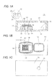
- Fig. 1A is a sectional view illustrating a structure of a conventional acoustic sensor
- Fig. 1B is a schematic plan view illustrating a state in which a cover of the acoustic sensor is removed
- Fig. 1C is a plan view illustrating a state in which the cover of the acoustic sensor is attached.
- an acoustic sensor 11 an acoustic sensing element 14 and a processing circuit unit 15 (IC chip) are accommodated in a casing including a base substrate 12 and a cover 13, a lower surface of the acoustic sensing element 14 is bonded to an upper surface of the base substrate 12 by a thermosetting bonding agent 24, and the processing circuit unit 15 is fixed by a bonding agent.
- the acoustic sensing element 14 includes a silicon substrate 16 in which a vertically-piercing back chamber 17 is formed, and a thin-film vibration electrode plate 18 is disposed opposite an upper surface opening of the back chamber 17 in an upper surface of the silicon substrate 16 and is covered with a fixed electrode plate 19 that is provided opposite the vibration electrode plate 18.
- a vibration electrode plate 18 In the vibration electrode plate 18, four corners are supported by leg portions 20, and a portion except the four corners is supported in the air by the upper surface of the silicon substrate 16.
- An opening 21 is formed in the cover 13 in order to guide an acoustic vibration into the casing, and a plurality of acoustic holes 22 are made in the fixed electrode plate 19 in order to guide the acoustic vibration to the vibration electrode plate 18.
- the acoustic vibration is converted into an electric signal and outputted based on an electrostatic capacitance change between the vibration electrode plate 18 and the fixed electrode plate 19.
- the vibration electrode plate 18 vibrates by resonating with the acoustic vibration, thereby generating the electrostatic capacitance change (for example, see International Patent Publication No. 2008-510427).
- the bonding agent 24 that is in the fluidized state immediately after application runs up the wall surface of the back chamber 17 by a surface tension to easily reach the upper surface of the silicon substrate 16.
- the bonding agent 24 easily runs up to the upper surface of the silicon substrate 16 along a valley fine (that is, an angular portion between sidewall surfaces of the back chamber 17).
- the bonding agent 24 When the bonding agent 24 runs up to the upper surface of the silicon substrate 16, the bonding agent 24 invades into a gap (vent hole 23) between the upper surface of the silicon substrate 16 and the lower surface in an edge portion of the vibration electrode plate 18, and a part of the vibration electrode plate 18, which should originally be floated from the silicon substrate 16, is stuck to the silicon substrate 16 to suppress the vibration of the vibration electrode plate 18.
- the vibration electrode plate 18 and the silicon substrate 16 are stuck by the run-up of the bonding agent 24, a distance between the fixed electrode plate 19 and the vibration electrode plate 18 is widened to decrease the electrostatic capacitance value, which causes sensitivity degradation of the acoustic sensor 11 or a characteristic change.
- the run-up of the bonding agent 24 When the run-up of the bonding agent 24 is prevented, a range of options of the bonding agent 24 is narrowed and cost is increased.
- the base substrate 12 is made of a hard material such as ceramic whose linear expansion coefficient is substantially equal to that of the silicon substrate 16.
- the ceramic substrate is expensive, and the cost of the acoustic sensor 11 is increased, Therefore, an organic substrate such as a resin substrate and a resin multi-layer substrate is generally used.
- the organic substrate significantly differs from the silicon substrate 16 of the acoustic sensing element 14 in the linear expansion coefficient, a thermal stress is generated between the silicon substrate 16 and the base substrate 12 by heat generation of the processing circuit unit 15 or external heat, which generates a risk of a warpage in the silicon substrate 16 and the base substrate 12. Therefore, a soft (low Young's modulus) bonding agent is used as the bonding agent 24 that bonds the lower surface of the silicon substrate 16 to the base substrate 12, and an internal stress generated between the base substrate 12 and the silicon substrate 16 is relaxed by the soft bonding agent 24.
- a soft (low Young's modulus) bonding agent is used as the bonding agent 24 that bonds the lower surface of the silicon substrate 16 to the base substrate 12, and an internal stress generated between the base substrate 12 and the silicon substrate 16 is relaxed by the soft bonding agent 24.
- the bonded portion between the silicon substrate 16 and the base substrate 12 has the flexible structure, and the silicon substrate 16 also has relatively low rigidity because the silicon substrate 16 is vertically pierced by the back chamber 17. Therefore, the silicon substrate 16 is easily deformed when the thermal stress is generated or when the external force is applied.
- the distance between the vibration electrode plate 18 and the fixed electrode plate 19 is decreased to degrade the sensitivity or the characteristic is changed, which results in a problem in that possibly the acoustic sensor 11 cannot be used. Therefore, the gap distance between the vibration electrode plate 18 and the fixed electrode plate 19 cannot extremely be decreased, which causes a restriction in improving the sensitivity of the acoustic sensor 11.
- the vibration electrode plate 18 When the silicon substrate 16 is deformed, a stress is unevenly generated in the vibration electrode plate 18 to decrease strength of the vibration electrode plate 18. Additionally, in order to sense the weak acoustic vibration with the acoustic sensor, it is necessary to extremely thin the vibration electrode plate 18. Therefore, the vibration electrode plate 13 is considerably brittle, and the vibration electrode plate 18 is easily broken by a drop of the acoustic sensor. Accordingly, in consideration of the strength, the thickness of the vibration electrode plate 18 is hardly decreased than ever before.
- the bonding agent 24 is peeled off to generate a bonding failure. Occasional a gap is generated between the lower surface of the silicon substrate 16 and the base substrate 12 by the bonding failure when the lower surface of the silicon substrate 16 is bonded to the base substrate 12 by the bonding agent 24.
- the bonding failure is generated, the acoustic vibration invades from the gap to reduce a difference in sound pressure between a surface and a rear surface of the vibration electrode plate 18, which degrades the sensitivity of the acoustic sensor 11.
- the present invention has been devised to solve the problems described above, and an object thereof is to prevent the phenomenon in which the bonding agent that fixes the acoustic sensing element to the base substrate runs up through the back chamber. Another object of the present invention is to prevent the leakage of the back chamber from the lower surface of the acoustic sensing element. Still another object of the present invention is to reduce the deformation of the acoustic sensing elements to improve the sensitivity of the acoustic sensor.
- an acoustic sensing element including a substrate that includes a back chamber, a vibration electrode plate that is provided in a surface of the substrate while being opposite an upper surface opening of the back chamber, and a fixed electrode plate that is provided opposite the vibration electrode plate, an acoustic hole being made in the fixed electrode plate, wherein the acoustic sensing element outputs an electric signal based on an electrostatic capacitance change generated between the vibration electrode plate and the fixed electrode plate by a displacement of the vibration electrode plate, and a slower surface of the back chamber is closed into a pouched shape by the substrate.
- the vibration electrode plate can be prevented from being stuck to the element substrate by the bonding agent, a vibration characteristic of the vibration electrode plate can be stabilized, and the sensitivity degradation of the acoustic sensor can be prevented while reliability is improved.
- the rigidity of the element substrate is improved, an impact resistance of the acoustic sensing element is improved.
- the vibration electrode plate is hardly broken by a drop impact, the vibration electrode plate can be thinned to improve the sensitivity of the acoustic sensing element.
- the acoustic sensing element is hardly deformed by the thermal stress or the external force, and the sensitivity degradation or the characteristic change can be prevented. Therefore, the gap between the vibration electrode plate and the fixed electrode plate can be narrowed to improve the sensitivity of the acoustic sensing element.
- the substrate is formed by joining a sub-substrate to a rear surface of a main substrate having a through-hole that pierces the main substrate from a surface to the rear surface, and a lower surface of the through-hole is closed by the sub-substrate, thereby forming the back chamber by a space including the through-hole.
- the back chamber whose lower surface side is closed can be prepared by simply joining the main substrate in which the through-hole is made to the rear surface of the sub-substrate, which facilitates the producing process.
- a recess may be formed in the sub-substrate while communicated with the through-hole, and the back chamber may be formed by the through-hole and the recess.
- a volume of the back chamber can be formed larger than that of the case where the back chamber is formed only by the through-hole, and the sensitivity of the acoustic sensing element can be improved.
- the main substrate and the sub-substrate are desirably joined by a method in which a bonding agent is not used. Because the substrates are joined with no use of the bonding agent, the bonding agent does not run up the through-hole of the main substrate to adhere to the vibration electrode plate, and therefore the reliability of the acoustic sensing element is enhanced while the yield is improved in the production.
- the main substrate and the sub-substrate are desirably made of materials whose linear expansion coefficients are substantially equal to each other.
- the warpage is hardly generated between the main substrate and the sub-substrate by a temperature change, the gap between the vibration electrode plate and the fixed electrode plate is hardly changed, and a temperature characteristic of the acoustic sensing element is stabilized.
- the vibration electrode plate is hardly stuck to the fixed electrode plate by the warpage.
- an acoustic sensor wherein a lower surface of the acoustic sensing element according to the present invention is stuck to an upper surface of a base substrate by a bonding agent, and a cover is attached to the upper surface of the base substrate such that the acoustic sensing element is covered therewith.
- the means for solving the problem in the present invention has the feature in which the above-described constituents are properly combined, and many variations can be made in the present invention by the combination of the constituents.
- Fig. 1A is a sectional view illustrating a structure of a conventional acoustic sensor
- Fig. 2 is a schematic sectional view of the acoustic sensor 31.
- the acoustic sensor 31 mainly includes an acoustic sensing element 32 and a circuit element 33 (IC chip). Lower surfaces of the acoustic sensing element 32 and circuit element 33 are bonded to an upper surface of a base substrate 34, in which a wiring pattern is formed, by a thermosetting bonding agent (thermosetting resin bonding agent).
- the acoustic sensing element 32 and the circuit elements 33 are covered with an electromagnetic shielding cover 35 joined to the upper surface of the base substrate 34, and the acoustic sensing element 32 and the circuit element 33 are accommodated in a space 36 that is formed by the base substrate 34 and the cover 35.
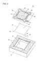
- Fig. 3 is an exploded perspective view illustrating a structure of the acoustic sensing element 32.
- the acoustic sensing element 32 is a micro electrostatic capacitance type element (MEMS transducer) that is prepared by utilizing the MEMS (Micro Electro Mechanical Systems) technology,
- MEMS Micro Electro Mechanical Systems
- a vibration electrode plate 43 is provided in an upper surface of an element substrate 41 that is of a silicon substrate with an insulating film 42 interposed therebetween, and a fixed electrode plate 44 is provided on the vibration electrode plate 43 with a microgap (void) interposed therebetween.
- the element substrate 41 includes a back chamber 45 that is recessed from a surface toward a rear surface by wet etching.
- the back chamber 45 does not reach the lower surface of the element substrate 41, and the back chamber 45 is opened only in the upper surface of the element substrate 41 white closed into a pouched shape in the lower surface of the element substrate 41.
- An inner peripheral surface of the back chamber 45 may vertically be formed or tapered.
- the elements substrate 41 is formed into a square of about 1 to about 1.5 mm (or less) when viewed from above, and a thickness ranges from about 400 to about 500 ⁇ m.
- An insulating film 42 made of an oxide film (SiO 2 film) is formed by the upper surface of the elements substrate 41.
- the vibration electrode plate 43 is formed by a polysilicon thin film having a thickness of about 1 ⁇ m.
- the vibration electrode plate 43 is a thin film having a substantially rectangular shape, and support legs 47 are diagonally extended toward the outside in four corner portions of the vibration electrode plate 43.
- An extended portion 48 is extended from one of the support legs 47.
- the vibration electrode plate 43 is disposed in the upper surface of the element substrate 41 such that the upper surface of the back chamber 45 is covered therewith, and the support legs 47 in the four corners and the extended portion 48 are fixed onto the insulating film 42.
- a portion in the first embodiment, a portion except the support legs 47 and the extended portion 48) that is supported in the air above the back chamber 45 constitutes a diaphragm 49 (vibration film), and the diaphragm 49 vibrates according to an acoustic vibration (air vibration).
- a fixed electrode 51 made of a metallic thin film is provided in an upper surface of a back plate 50 made of a nitride film.
- the diaphragm 49 is covered with the fixed electrode plate 44 with a micro gap of about 3 ⁇ m, and the fixed electrode 51 is disposed opposite the diaphragm 49 to constitute a capacitor.
- An outer peripheral portion of the fixed electrode plate 44, that is, an outside portion of a region that is opposite the diaphragm 49 is fixed to the upper surface of the element substrate 41 while the insulating film 42 made of an oxide film is interposed therebetween.
- a lead-out portion 52 is extended from the fixed electrode 51, and an electrode pad 53 (Au film) that is electrically conducted to the fixed electrode 51 is provided at a leading end of the lead-out portion 52.
- An electrode pad 54 (Au film) is provided in the fixed electrode plate 44.
- the electrode pad 54 is joined to the extended portion 48 of the vibration electrode plate 43 to electrically conduct the extended portion 48 to the vibration electrode plate 43.
- the electrode pad 53 is disposed in the upper surface of the back plate 50, and the electrode pad 54 is joined to the extended portion 48 through an opening of the back plate 50.
- the vibration electrode plate 43 In order to pass the acoustic vibration, many acoustic holes 55 are made in the fixed electrode 51 and the back plate 50 so as to be pierced from the upper surface to the lower surface. Because the vibration electrode plate 43 resonates with the acoustic vibration or the mechanical vibration to vibrate, the vibration electrode plate 43 is made of a thin film having a thickness of about 1 ⁇ m. On the other hand, because the fixed electrode plate 44 is the electrode that is not excited by the acoustic vibration or the mechanical vibration, the fixed electrode plate 44 has a thickness of 2 ⁇ m or more.
- the whole rear surface of the acoustic sensing element 32 is jointed to the upper surface of the base substrate 34 by a bonding agent 56 made of a thermosetting resin.
- the circuit element 33 that processes an output signal of the acoustic sensing elements 32 is also bonded to the upper surface of the base substrate 34 by a thermosetting resin.
- the acoustic sensing element 32 and the circuit element 33 are connected through wiring pattern of the base substrate 34 by a bonding wire.
- the cover 35 has an electromagnetic shielding function of cutting off an electromagnetic noise from the outside. Therefore, the cover 35 may be made of a conductive metal, or an inner surface of a resin cover may be covered with a metallic film by plating. An opening 57 is formed in the cover 35, and the space 36 between the opening 57 and the acoustic hole 55 constitutes a pathway through which the acoustic vibration propagates. In the base substrate 34, a part of a grounding wiring pattern also has the electromagnetic shielding function.
- the acoustic vibration propagates into the space 36 through the opening 57 of the cover 35 and propagates into the acoustic sensing element 32 through the acoustic hole 55, whereby the diaphragm 49 vibrates by the acoustic vibration.
- the diaphragm 49 vibrates, a gap distance between the diaphragm 49 and the fixed electrode plate 44 is changed, and therefore an electrostatic capacitance between the diaphragm 49 and the fixed electrode 51 is changed. Accordingly, when the change in electrostatic capacitance is extracted as an electric signal while a DC voltage is applied between the electrode pads 53 and 54, the acoustic vibration can be detected by converting the acoustic vibration into the electric signal.
- the bonding agent 56 that is in the fluidized state before the curing does not run up the wall surface of the back chamber 45 by the surface tension.
- the bonding agent 56 invades into the gap (vent hole) between the upper surface of the element substrate 41 and the vibration electrode plate 43 to stick the vibration electrode plate 43 to the element substrate 41 is eliminated unlike the conventional technology.
- the sticking of the vibration electrode plate 43 to the element substrate 41 can be prevented to stabilize the vibration characteristic of the diaphragm 49, and the reliability can be improved while the sensitivity degradation of the acoustic sensor 31 is prevented.
- the bonding agent 56 does not run up the back chamber 45, so that the range of options of the bonding agent 24 can be broadened to reduce the cost of the acoustic sensor 31.
- the acoustic vibration does not invade from the lower surface of the acoustic sensing element 32 by the leakage of the back chamber 45. Therefore, the sensitivity degradation of the acoustic sensor 31 due to the leakage can be prevented to improve the yield in the sensor producing process.
- the vibration electrode plate 43 can be supported by the element substrate 41 having the high rigidity, the impact resistance of the acoustic sensing element 32 is improved, and the acoustic sensing element 32 and the vibration electrode plate 43 is hardly broken by the drop impact,
- the rigidity of the element substrate 41 is increased, the acoustic sensing element 32 is hardly deformed even if the thermal stress is generated or the external force is applied. Therefore, the gap between the vibration electrode plate 43 and the fixed electrode plate 44 is hardly changed, so that the sensitivity degradation of the acoustic sensor 31 and the characteristic change can be prevented.
- the diaphragm 49 can be thinned, the gap between the vibration electrode plate 43 and the fixed electrode plate 44 can be narrowed, and the sensitivity of the acoustic sensor 31 can be improved.
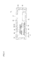
- Fig. 4 is a schematic sectional view illustrating an acoustic sensor 61 according to a second embodiment of the present invention.
- the acoustic sensor 61 differs from the acoustic sensor 31 of the first embodiment in the structure of the element substrate 41
- Fig. 5 is an exploded perspective view illustrating a structure of the element substrate 41 of the second embodiment.
- one silicon substrate is etched into a concave shape to form the back chamber 45 whose lower surface is closed in the element substrate 41.
- a sub-substrate 41 b is joined to a rear surface of a main substrate 41 a to form the element substrate 41 as illustrated in Fig. 5 .
- the main substrate 41 a is formed by a silicon substrate or an SOI (Silicon On Insulator) substrate, and the back chamber 45 is formed in the main substrate 41a while the main substrate 41a is pierced from the surface to the rear surface.
- the surface of the sub-substrate 41 b is flattened.
- the silicon substrate and the SOI substrate which are similar to those of the main substrate 41 a or the glass substrate and the ceramic substrate such as Pyrex (registered trademark) and quartz which have linear expansion coefficients (about 2x10 -6 to about 10 x 10 -6 /°C) similar to those of the main substrate 41a are used as the sub-substrate 41 b.
- joining surfaces of the main substrate 41a made of Si and the sub-substrate 41 b made of Si are activated by a plasma treatment or the like, and the main substrate 41 a and the sub-substrate 41 b are joined at room temperature by applying a pressure while the joining surfaces are overlapped.
- the main substrate 41a and the sub-substrate 41b may be joined by heating and pressurization while a SiO 2 surface of the main substrate 41a made of the SOI and a SiO 2 surface of the sub-substrate 41 b made of the SOI are overlapped.
- the main substrate 41a made of Si and the sub-substrate 41b made of glass are overlapped, and a voltage may be applied to perform anodic bonding while the substrates 41a and 41b are heated and pressurized.
- metallic thin films made of Au or the like are deposited on the joining surfaces of the main substrate 41 a made of Si and the joining surface of the sub-substrate 41 b made of Si, the joining surfaces of the substrates 41 a and 41b may be joined by the heating and pressurization while overlapped.
- a hydrophilic treatment is performed to the joining surface (Al surface) of the sub-substrate 41 b made of Al (or the sub-substrate 41b made of the Si substrate in which an Al thin film is formed in the joining surface)
- the sub-substrate 41 b and the main substrate 41a made of Si are heated while overlapped, and the substrates 41a and 41 b may be joined using hydrogen bonding.
- the main substrate 41a and sub-substrate 41 b may be joined using the bonding agent made of an epoxy resin or an acrylic resin or a rubber agent which hardly oozes or runs up during the bonding.
- the joining material such as the bonding agent does not runs up the wall surface of the back chamber 45 to reach the upper surface of the main substrate 41a.
- the process of producing the element substrate 41 become simplified, when the main substrate 41a that is pierced by the back chamber 45 is joined to the sub-substrate 41 b to prepare the element substrate 41. That is, in the structure of the first embodiment, in order to form the back chamber 45 by the etching, it is necessary to carefully perform a time management of an etching depth such that the etching does not reach a bottom surface of the back chamber 45.
- the etching work of the back chamber 45 is facilitated because the main substrate 41 a is simply pierced by the back chamber 45, and the depth of the back chamber 45 can accurately be controlled because the depth of the back chamber 45 depends on the thickness of the main substrate 41a.
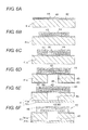
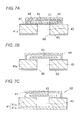
- Figs. 6A to 6F illustrate an example of a process of producing the acoustic sensing element
- the insulating film 42 SiO 2 film
- an opening 63 is formed while aligned with the back chamber opening position as illustrated in Fig. 6A
- a sacrifice layer 64 is stacked thereon. As illustrated in Fig.
- a polysilicon thin film is deposited on the sacrifice layer 64, the polysilicon thin film is formed into a predetermined shape to form the vibration electrode plate 43, the sacrifice layer 64 is stacked on the vibration electrode plate 43 again, and the sacrifice layer 64 is formed into a space shape in the fixed electrode plate 44. Then, the fixed electrode plate 44 (the back plate 50 and the fixed electrode 51) are formed on the sacrifice layer 64 and the insulating film 42 to make the acoustic holes 55 in the fixed electrode plate 44.
- Fig 6C illustrates this state.
- an etching mask 65 made of SiO 2 or SiN is deposited on the lower surface of the main substrate 41a, and an etching window 66 is opened in the etching mask 65.
- the main substrate 41 a is anisotropically etched from the lower surface through the etching window 66 by wet etching or dry etching, and the etching is stopped when the etching reaches the upper surface of the main substrate 41 a, whereby the back chamber 45 vertically pierces the main substrate 41a.
- the etching mask 65 of the lower surface is removed, the sub-substrate 41 b (wafer) is joined to the lower surface of the main substrate 41a by the above-described methods to form the element substrate 41.
- an etching solution is brought into contact with the sacrifice layer 64 through the acoustic holes 55 on the upper surface, and the sacrifice layer 64 in the fixed electrode plate 44 is removed by the etching, and the diaphragm 49 is floated from the upper surface of the main substrate 41a in the fixed electrode plate 44 to prepare the plurality of acoustic sensing elements 62 on one main substrate 41a (Si wafer).
- the element substrate 41 two joined wafers
- the acoustic sensing element 62 may be produced through a process illustrated in Figs. 7A to 7C.
- Fig. 7A illustrates the same state as that of Fig. 6D
- the vibration electrode plate 43, the sacrifice layer 64, and the fixed electrode plate 44 are provided on the upper surface of the main substrate 41a to form the back chamber 45 in the main substrate 41 a through the etching window 66 by the process illustrated in Figs. 6A to 6D .
- the etching solution is brought into contact with the sacrifice layer 64 through the acoustic holes 55 or the like on the upper surface
- the sacrifice layer 64 in the fixed electrode plate 44 is removed by the etching as illustrated in Fig. 7B
- the diaphragm 49 is floated from the upper surface of the main substrate 41a in the fixed electrode plate 44
- the plurality of acoustic sensing elements 62 are prepared on one main substrate 41a (Si wafer).
- the etching mask 65 of the lower surface is removed, and the sub-substrate 41b (wafer) is joined to the lower surface of the main substrate 41 a by the above-described methods to form the element substrate 41.
- the element substrate 41 is diced to cut out the acoustic sensing elements 62, thereby obtaining the individual acoustic sensing element 62.
- the back chamber 45 provided in the main substrate 41 a may be formed into any shape as long as the back chamber 45 can be prepared.
- the back chamber 45 in which an upper half is formed into a truncated-pyramid shape that is narrowed upward while a lower half is formed into an inverted truncated-pyramid shape that is narrowed downward, is formed in an acoustic sensor 68 according tao a modification of the second embodiment as illustrated in Fig. 8 .
- Fig. 9 is a schematic sectional view illustrating an acoustic sensor 71 according to a third embodiment of the present invention.
- the sub-substrate 41 b having the flat surface joined to the lower surface of the main substrate 41 a is used in the acoustic sensor 61 of the second embodiment.
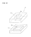
- a recess 45b is also formed in the sub-substrate 41 b as illustrated in Fig. 10 .
- the sub-substrate 41b in which the recess 45b is formed in the upper surface is joined to the lower surface of the main substrate 41 a having the through-hole 45a that pierces the main substrate from the surface to the rear surface, the element substrate 41 is formed by the main substrate 41 a and the sub-substrate 41 b, and the back chamber 45 is formed by the through-hole 45a and recess 45b, which are communicated with each other.
- the acoustic sensing element 62 of the third embodiment can be produced similarly to the second embodiment, and the method similar to that of the second embodiment can be adopted in the method for joining the main substrate 41a and the sub-substrate 41b.
- a volume of the back chamber 45 is further enlarged by providing the recess 45b in the sub-substrate 41 b, so that sensitivity of the acoustic sensor 71 can be improved.
- the recess 45b may be formed into a shape in which each corner become angular as illustrated in Fig. 10 , or may be formed into a shape in which each corner is rounded as illustrated in Fig. 11 .
- the recess 45b When a diameter of the upper surface opening of the recess 45b is larger than a diameter of the slower surface opening of the through-hole 45a, the recess 45b can be enlarged to increase the volume of the back chamber 45. Therefore., the sensitivity of the acoustic sensing element 32 can be improved.
- the through-hole 45a made in the main substrate 41 a and the recess 45b provided in the sub-substrate 41 b can be formed into various shapes in the third embodiment.
- the recess 45b having the inverted truncated-pyramid shape illustrated in Fig. 12B is provided while communicated with the lower surface of the through-hole 45a having the prismatic shape.
- the recess 45b having the spherical shape illustrated in Fig. 13B is provided while communicated with the lower surface of the through-hole 45a having the prismatic shape.
- the recesses 45b having the rectangular, inverted truncated-pyramid, and spherical shapes are provided in acoustic sensing elements 74 to 76 illustrated in Figs. 14A to 14C while communicated with the lower surface of the through-hole 45a having the truncated-pyramid shape that is narrowed upward, respectively.
- the recesses 45b having the rectangular, inverted truncated-pyramid, and spherical shapes are provided in acoustic sensing elements 77 to 79 illustrated in Figs.
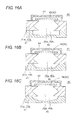
- the recesses 45b having the rectangular, inverted truncated-pyramid, and spherical shapes are provided in acoustic sensing elements 80 to 82 illustrated in Figs. 16A to 16C while communicated with the lower surface of the through-hole 45a having the shape in which the upper half is formed into the truncated-pyramid shape narrowed upward while the lower half is formed into the inverted truncated-pyramid shape narrowed downward, respectively.
Landscapes
- Engineering & Computer Science (AREA)
- Manufacturing & Machinery (AREA)
- Physics & Mathematics (AREA)
- Acoustics & Sound (AREA)
- Signal Processing (AREA)
- Microelectronics & Electronic Packaging (AREA)
- General Physics & Mathematics (AREA)
- Electrostatic, Electromagnetic, Magneto- Strictive, And Variable-Resistance Transducers (AREA)
- Measurement Of Mechanical Vibrations Or Ultrasonic Waves (AREA)
- Pressure Sensors (AREA)
- Details Of Audible-Bandwidth Transducers (AREA)
Applications Claiming Priority (1)
| Application Number | Priority Date | Filing Date | Title |
|---|---|---|---|
| JP2010038289A JP4947168B2 (ja) | 2010-02-24 | 2010-02-24 | 音響センサ |
Publications (2)
| Publication Number | Publication Date |
|---|---|
| EP2360942A2 true EP2360942A2 (fr) | 2011-08-24 |
| EP2360942A3 EP2360942A3 (fr) | 2012-03-28 |
Family
ID=44065016
Family Applications (1)
| Application Number | Title | Priority Date | Filing Date |
|---|---|---|---|
| EP10196842A Ceased EP2360942A3 (fr) | 2010-02-24 | 2010-12-23 | Capteur acoustique |
Country Status (5)
| Country | Link |
|---|---|
| US (1) | US8300857B2 (fr) |
| EP (1) | EP2360942A3 (fr) |
| JP (1) | JP4947168B2 (fr) |
| KR (1) | KR101205645B1 (fr) |
| CN (1) | CN102164333A (fr) |
Cited By (1)
| Publication number | Priority date | Publication date | Assignee | Title |
|---|---|---|---|---|
| ITTO20130247A1 (it) * | 2013-03-26 | 2014-09-27 | St Microelectronics Srl | Metodo di incapsulamento di un dispositivo trasduttore mems e dispositivo trasduttore mems incapsulato |
Families Citing this family (16)
| Publication number | Priority date | Publication date | Assignee | Title |
|---|---|---|---|---|
| JP5454345B2 (ja) * | 2010-05-11 | 2014-03-26 | オムロン株式会社 | 音響センサ及びその製造方法 |
| US8969980B2 (en) * | 2011-09-23 | 2015-03-03 | Knowles Electronics, Llc | Vented MEMS apparatus and method of manufacture |
| US20130101143A1 (en) * | 2011-10-21 | 2013-04-25 | Hung-Jen Chen | Micro-electro-mechanical system microphone chip with an expanded back chamber |
| JP2013143651A (ja) * | 2012-01-10 | 2013-07-22 | Nippon Dempa Kogyo Co Ltd | ディスク振動子及び電子部品 |
| JP5861497B2 (ja) * | 2012-02-29 | 2016-02-16 | オムロン株式会社 | センサ装置 |
| US9491531B2 (en) | 2014-08-11 | 2016-11-08 | 3R Semiconductor Technology Inc. | Microphone device for reducing noise coupling effect |
| JP2016058880A (ja) * | 2014-09-09 | 2016-04-21 | 晶▲めい▼電子股▲ふん▼有限公司 | ノイズカップリングの影響を低減させるマイクロフォン装置 |
| WO2016043738A1 (fr) * | 2014-09-17 | 2016-03-24 | Intel Corporation | Microplaquette à microphone intégré au moyen d'interconnexions verticales (tsv) |
| US10648879B2 (en) * | 2016-02-22 | 2020-05-12 | Kathirgamasundaram Sooriakumar | Capacitive pressure sensor |
| JP2019106616A (ja) * | 2017-12-12 | 2019-06-27 | 新日本無線株式会社 | Mems素子 |
| KR102486584B1 (ko) * | 2018-05-03 | 2023-01-10 | 주식회사 디비하이텍 | 멤스 마이크로폰, 이를 포함하는 멤스 마이크로폰 패키지 및 이의 제조 방법 |
| KR102499855B1 (ko) * | 2018-05-03 | 2023-02-13 | 주식회사 디비하이텍 | 멤스 마이크로폰 이를 포함하는 멤스 마이크로폰 패키지 및 이의 제조 방법 |
| JP2020022038A (ja) * | 2018-07-31 | 2020-02-06 | Tdk株式会社 | Memsマイクロフォン |
| CN111189531B (zh) * | 2020-03-09 | 2025-01-24 | 西南交通大学 | 一种用于正弦波面样品轻气炮加载试验的检测系统 |
| US11787690B1 (en) | 2020-04-03 | 2023-10-17 | Knowles Electronics, Llc. | MEMS assembly substrates including a bond layer |
| CN112146789A (zh) * | 2020-09-15 | 2020-12-29 | 南京慧卉飞电子商务有限公司 | 一种利用磁流变液的智能化音响检测装置 |
Citations (4)
| Publication number | Priority date | Publication date | Assignee | Title |
|---|---|---|---|---|
| JP2008510427A (ja) | 2004-08-19 | 2008-04-03 | ノールズ エレクトロニクス エルエルシー | シリコンコンデンサーマイクロホンおよびその製造方法 |
| US20080157301A1 (en) * | 2007-01-03 | 2008-07-03 | Stats Chippac, Inc. | Leadframe package for mems microphone assembly |
| US20090001553A1 (en) * | 2005-11-10 | 2009-01-01 | Epcos Ag | Mems Package and Method for the Production Thereof |
| WO2009031742A1 (fr) * | 2007-09-03 | 2009-03-12 | Bse Co., Ltd. | Microphone à condensateur utilisant un emballage céramique dont l'intérieur est entouré de métal ou de matériaux conducteurs |
Family Cites Families (13)
| Publication number | Priority date | Publication date | Assignee | Title |
|---|---|---|---|---|
| US6522762B1 (en) * | 1999-09-07 | 2003-02-18 | Microtronic A/S | Silicon-based sensor system |
| JP2002345088A (ja) * | 2001-05-18 | 2002-11-29 | Mitsubishi Electric Corp | 圧力感応装置及びこれに用いられる半導体基板の製造方法 |
| WO2005086535A1 (fr) * | 2004-03-09 | 2005-09-15 | Matsushita Electric Industrial Co., Ltd. | Microphone a condensateur a electret |
| CN1728888A (zh) * | 2004-07-30 | 2006-02-01 | 三洋电机株式会社 | 声敏元件 |
| JP4539450B2 (ja) * | 2004-11-04 | 2010-09-08 | オムロン株式会社 | 容量型振動センサ及びその製造方法 |
| JP4188325B2 (ja) * | 2005-02-09 | 2008-11-26 | ホシデン株式会社 | 防塵板内蔵マイクロホン |
| JP4742972B2 (ja) * | 2006-04-27 | 2011-08-10 | オムロン株式会社 | マイクロフォンの製造方法 |
| TWI319690B (en) * | 2006-09-08 | 2010-01-11 | Ind Tech Res Inst | Structure and manufacturing method of inversed microphone module and microphone chip component |
| JP2008278476A (ja) | 2007-04-05 | 2008-11-13 | Yamaha Corp | コンデンサマイク装置のsn比改善方法およびコンデンサマイク装置並びにコンデンサマイク装置搭載機器 |
| CN101828310B (zh) | 2007-10-19 | 2013-04-03 | 日本发条株式会社 | 连接端子、半导体封装、布线基板、连接器及微接触器 |
| CN101426164B (zh) * | 2007-11-01 | 2012-10-03 | 财团法人工业技术研究院 | 电声感知装置 |
| JP2009246779A (ja) * | 2008-03-31 | 2009-10-22 | Funai Electric Advanced Applied Technology Research Institute Inc | マイクロホンユニット及びその製造方法 |
| EP2252077B1 (fr) * | 2009-05-11 | 2012-07-11 | STMicroelectronics Srl | Ensemble de transducteur acoustique capacitif de type micro-électromécanique et paquet correspondant |
-
2010
- 2010-02-24 JP JP2010038289A patent/JP4947168B2/ja not_active Expired - Fee Related
- 2010-12-23 EP EP10196842A patent/EP2360942A3/fr not_active Ceased
-
2011
- 2011-01-04 KR KR1020110000372A patent/KR101205645B1/ko active Active
- 2011-01-10 CN CN2011100033783A patent/CN102164333A/zh active Pending
- 2011-01-28 US US13/016,436 patent/US8300857B2/en active Active
Patent Citations (4)
| Publication number | Priority date | Publication date | Assignee | Title |
|---|---|---|---|---|
| JP2008510427A (ja) | 2004-08-19 | 2008-04-03 | ノールズ エレクトロニクス エルエルシー | シリコンコンデンサーマイクロホンおよびその製造方法 |
| US20090001553A1 (en) * | 2005-11-10 | 2009-01-01 | Epcos Ag | Mems Package and Method for the Production Thereof |
| US20080157301A1 (en) * | 2007-01-03 | 2008-07-03 | Stats Chippac, Inc. | Leadframe package for mems microphone assembly |
| WO2009031742A1 (fr) * | 2007-09-03 | 2009-03-12 | Bse Co., Ltd. | Microphone à condensateur utilisant un emballage céramique dont l'intérieur est entouré de métal ou de matériaux conducteurs |
Cited By (2)
| Publication number | Priority date | Publication date | Assignee | Title |
|---|---|---|---|---|
| ITTO20130247A1 (it) * | 2013-03-26 | 2014-09-27 | St Microelectronics Srl | Metodo di incapsulamento di un dispositivo trasduttore mems e dispositivo trasduttore mems incapsulato |
| US9321626B2 (en) | 2013-03-26 | 2016-04-26 | Stmicroelectronics S.R.L. | Method of packaging a MEMS transducer device and packaged MEMS transducer device |
Also Published As
| Publication number | Publication date |
|---|---|
| JP4947168B2 (ja) | 2012-06-06 |
| JP2011176531A (ja) | 2011-09-08 |
| KR20110097614A (ko) | 2011-08-31 |
| KR101205645B1 (ko) | 2012-11-27 |
| US8300857B2 (en) | 2012-10-30 |
| CN102164333A (zh) | 2011-08-24 |
| EP2360942A3 (fr) | 2012-03-28 |
| US20110204745A1 (en) | 2011-08-25 |
Similar Documents
| Publication | Publication Date | Title |
|---|---|---|
| US8300857B2 (en) | Acoustic sensor | |
| EP1860417B1 (fr) | Capteur de pression comportant une chambre et procédé de fabrication de celui-ci | |
| US8983105B2 (en) | Microphone | |
| TWI504279B (zh) | Mems音波感測器及其製造方法 | |
| JP5763682B2 (ja) | Mems及びasicを備える小型化した電気的デバイス及びその製造方法 | |
| CN102244829B (zh) | 声音传感器及其制造方法 | |
| US20070275495A1 (en) | Method for fabricating a pressure sensor using SOI wafers | |
| TW200532746A (en) | Electronic component, electronic component module and method of manufacturing the electronic component | |
| KR101761967B1 (ko) | 평면 형태를 가진 전기 소자 및 그 제조 방법 | |
| GB2452650A (en) | MEMS microphone | |
| JP2008271425A (ja) | 音響センサおよびその製造方法 | |
| JP2009291514A (ja) | 静電容量型トランスデューサの製造方法、及び静電容量型トランスデューサ | |
| JP2005201818A (ja) | 圧力センサ | |
| WO2012114538A1 (fr) | Procédé pour fabriquer un dispositif à semi-conducteurs et procédé pour fabriquer un microphone | |
| JP2016015723A (ja) | トランスデューサ、及び測定装置 | |
| US10190930B2 (en) | Micro feedback-chamber sensor and method of manufacturing such sensor | |
| CN101437187A (zh) | 用以减缩微型传感器封装体积的堆叠式封装结构 | |
| JP2012006092A (ja) | Memsデバイス及びその製造方法並びにmemsデバイスを有するパッケージ | |
| CN117664199A (zh) | 具有声耦合介质的传感装置和相应的制造方法 | |
| CN111174957A (zh) | 一种压力传感器及制备方法 | |
| JP2008271424A (ja) | 音響センサ | |
| US20220080461A1 (en) | Micromechanical component for a sound transducer and corresponding production method | |
| JP5771921B2 (ja) | 封止型デバイス及びその製造方法 | |
| JP5843302B1 (ja) | 複合センサデバイスの製造方法 | |
| WO2010008344A2 (fr) | Volume arrière de capteur étendu |
Legal Events
| Date | Code | Title | Description |
|---|---|---|---|
| PUAI | Public reference made under article 153(3) epc to a published international application that has entered the european phase |
Free format text: ORIGINAL CODE: 0009012 |
|
| AK | Designated contracting states |
Kind code of ref document: A2 Designated state(s): AL AT BE BG CH CY CZ DE DK EE ES FI FR GB GR HR HU IE IS IT LI LT LU LV MC MK MT NL NO PL PT RO RS SE SI SK SM TR |
|
| AX | Request for extension of the european patent |
Extension state: BA ME |
|
| RAP1 | Party data changed (applicant data changed or rights of an application transferred) |
Owner name: OMRON CORPORATION |
|
| RTI1 | Title (correction) |
Free format text: ACOUSTIC SENSOR |
|
| PUAL | Search report despatched |
Free format text: ORIGINAL CODE: 0009013 |
|
| AK | Designated contracting states |
Kind code of ref document: A3 Designated state(s): AL AT BE BG CH CY CZ DE DK EE ES FI FR GB GR HR HU IE IS IT LI LT LU LV MC MK MT NL NO PL PT RO RS SE SI SK SM TR |
|
| AX | Request for extension of the european patent |
Extension state: BA ME |
|
| RIC1 | Information provided on ipc code assigned before grant |
Ipc: H04R 19/00 20060101AFI20120220BHEP Ipc: H04R 19/04 20060101ALN20120220BHEP |
|
| 17P | Request for examination filed |
Effective date: 20120724 |
|
| 17Q | First examination report despatched |
Effective date: 20130620 |
|
| STAA | Information on the status of an ep patent application or granted ep patent |
Free format text: STATUS: EXAMINATION IS IN PROGRESS |
|
| STAA | Information on the status of an ep patent application or granted ep patent |
Free format text: STATUS: THE APPLICATION HAS BEEN REFUSED |
|
| 18R | Application refused |
Effective date: 20180920 |