EP2362003B1 - Procédé pour déposer des films de SiO2 - Google Patents
Procédé pour déposer des films de SiO2 Download PDFInfo
- Publication number
- EP2362003B1 EP2362003B1 EP10275131.0A EP10275131A EP2362003B1 EP 2362003 B1 EP2362003 B1 EP 2362003B1 EP 10275131 A EP10275131 A EP 10275131A EP 2362003 B1 EP2362003 B1 EP 2362003B1
- Authority
- EP
- European Patent Office
- Prior art keywords
- teos
- film
- plasma
- frequency component
- plasma treatment
- Prior art date
- Legal status (The legal status is an assumption and is not a legal conclusion. Google has not performed a legal analysis and makes no representation as to the accuracy of the status listed.)
- Active
Links
Images


Classifications
-
- C—CHEMISTRY; METALLURGY
- C23—COATING METALLIC MATERIAL; COATING MATERIAL WITH METALLIC MATERIAL; CHEMICAL SURFACE TREATMENT; DIFFUSION TREATMENT OF METALLIC MATERIAL; COATING BY VACUUM EVAPORATION, BY SPUTTERING, BY ION IMPLANTATION OR BY CHEMICAL VAPOUR DEPOSITION, IN GENERAL; INHIBITING CORROSION OF METALLIC MATERIAL OR INCRUSTATION IN GENERAL
- C23C—COATING METALLIC MATERIAL; COATING MATERIAL WITH METALLIC MATERIAL; SURFACE TREATMENT OF METALLIC MATERIAL BY DIFFUSION INTO THE SURFACE, BY CHEMICAL CONVERSION OR SUBSTITUTION; COATING BY VACUUM EVAPORATION, BY SPUTTERING, BY ION IMPLANTATION OR BY CHEMICAL VAPOUR DEPOSITION, IN GENERAL
- C23C16/00—Chemical coating by decomposition of gaseous compounds, without leaving reaction products of surface material in the coating, i.e. chemical vapour deposition [CVD] processes
- C23C16/22—Chemical coating by decomposition of gaseous compounds, without leaving reaction products of surface material in the coating, i.e. chemical vapour deposition [CVD] processes characterised by the deposition of inorganic material, other than metallic material
- C23C16/30—Deposition of compounds, mixtures or solid solutions, e.g. borides, carbides, nitrides
- C23C16/40—Oxides
- C23C16/401—Oxides containing silicon
- C23C16/402—Silicon dioxide
-
- C—CHEMISTRY; METALLURGY
- C23—COATING METALLIC MATERIAL; COATING MATERIAL WITH METALLIC MATERIAL; CHEMICAL SURFACE TREATMENT; DIFFUSION TREATMENT OF METALLIC MATERIAL; COATING BY VACUUM EVAPORATION, BY SPUTTERING, BY ION IMPLANTATION OR BY CHEMICAL VAPOUR DEPOSITION, IN GENERAL; INHIBITING CORROSION OF METALLIC MATERIAL OR INCRUSTATION IN GENERAL
- C23C—COATING METALLIC MATERIAL; COATING MATERIAL WITH METALLIC MATERIAL; SURFACE TREATMENT OF METALLIC MATERIAL BY DIFFUSION INTO THE SURFACE, BY CHEMICAL CONVERSION OR SUBSTITUTION; COATING BY VACUUM EVAPORATION, BY SPUTTERING, BY ION IMPLANTATION OR BY CHEMICAL VAPOUR DEPOSITION, IN GENERAL
- C23C16/00—Chemical coating by decomposition of gaseous compounds, without leaving reaction products of surface material in the coating, i.e. chemical vapour deposition [CVD] processes
- C23C16/44—Chemical coating by decomposition of gaseous compounds, without leaving reaction products of surface material in the coating, i.e. chemical vapour deposition [CVD] processes characterised by the method of coating
- C23C16/455—Chemical coating by decomposition of gaseous compounds, without leaving reaction products of surface material in the coating, i.e. chemical vapour deposition [CVD] processes characterised by the method of coating characterised by the method used for introducing gases into reaction chamber or for modifying gas flows in reaction chamber
- C23C16/45563—Gas nozzles
- C23C16/45565—Shower nozzles
-
- C—CHEMISTRY; METALLURGY
- C23—COATING METALLIC MATERIAL; COATING MATERIAL WITH METALLIC MATERIAL; CHEMICAL SURFACE TREATMENT; DIFFUSION TREATMENT OF METALLIC MATERIAL; COATING BY VACUUM EVAPORATION, BY SPUTTERING, BY ION IMPLANTATION OR BY CHEMICAL VAPOUR DEPOSITION, IN GENERAL; INHIBITING CORROSION OF METALLIC MATERIAL OR INCRUSTATION IN GENERAL
- C23C—COATING METALLIC MATERIAL; COATING MATERIAL WITH METALLIC MATERIAL; SURFACE TREATMENT OF METALLIC MATERIAL BY DIFFUSION INTO THE SURFACE, BY CHEMICAL CONVERSION OR SUBSTITUTION; COATING BY VACUUM EVAPORATION, BY SPUTTERING, BY ION IMPLANTATION OR BY CHEMICAL VAPOUR DEPOSITION, IN GENERAL
- C23C16/00—Chemical coating by decomposition of gaseous compounds, without leaving reaction products of surface material in the coating, i.e. chemical vapour deposition [CVD] processes
- C23C16/44—Chemical coating by decomposition of gaseous compounds, without leaving reaction products of surface material in the coating, i.e. chemical vapour deposition [CVD] processes characterised by the method of coating
- C23C16/50—Chemical coating by decomposition of gaseous compounds, without leaving reaction products of surface material in the coating, i.e. chemical vapour deposition [CVD] processes characterised by the method of coating using electric discharges
- C23C16/505—Chemical coating by decomposition of gaseous compounds, without leaving reaction products of surface material in the coating, i.e. chemical vapour deposition [CVD] processes characterised by the method of coating using electric discharges using radio frequency discharges
-
- C—CHEMISTRY; METALLURGY
- C23—COATING METALLIC MATERIAL; COATING MATERIAL WITH METALLIC MATERIAL; CHEMICAL SURFACE TREATMENT; DIFFUSION TREATMENT OF METALLIC MATERIAL; COATING BY VACUUM EVAPORATION, BY SPUTTERING, BY ION IMPLANTATION OR BY CHEMICAL VAPOUR DEPOSITION, IN GENERAL; INHIBITING CORROSION OF METALLIC MATERIAL OR INCRUSTATION IN GENERAL
- C23C—COATING METALLIC MATERIAL; COATING MATERIAL WITH METALLIC MATERIAL; SURFACE TREATMENT OF METALLIC MATERIAL BY DIFFUSION INTO THE SURFACE, BY CHEMICAL CONVERSION OR SUBSTITUTION; COATING BY VACUUM EVAPORATION, BY SPUTTERING, BY ION IMPLANTATION OR BY CHEMICAL VAPOUR DEPOSITION, IN GENERAL
- C23C16/00—Chemical coating by decomposition of gaseous compounds, without leaving reaction products of surface material in the coating, i.e. chemical vapour deposition [CVD] processes
- C23C16/44—Chemical coating by decomposition of gaseous compounds, without leaving reaction products of surface material in the coating, i.e. chemical vapour deposition [CVD] processes characterised by the method of coating
- C23C16/52—Controlling or regulating the coating process
-
- C—CHEMISTRY; METALLURGY
- C23—COATING METALLIC MATERIAL; COATING MATERIAL WITH METALLIC MATERIAL; CHEMICAL SURFACE TREATMENT; DIFFUSION TREATMENT OF METALLIC MATERIAL; COATING BY VACUUM EVAPORATION, BY SPUTTERING, BY ION IMPLANTATION OR BY CHEMICAL VAPOUR DEPOSITION, IN GENERAL; INHIBITING CORROSION OF METALLIC MATERIAL OR INCRUSTATION IN GENERAL
- C23C—COATING METALLIC MATERIAL; COATING MATERIAL WITH METALLIC MATERIAL; SURFACE TREATMENT OF METALLIC MATERIAL BY DIFFUSION INTO THE SURFACE, BY CHEMICAL CONVERSION OR SUBSTITUTION; COATING BY VACUUM EVAPORATION, BY SPUTTERING, BY ION IMPLANTATION OR BY CHEMICAL VAPOUR DEPOSITION, IN GENERAL
- C23C16/00—Chemical coating by decomposition of gaseous compounds, without leaving reaction products of surface material in the coating, i.e. chemical vapour deposition [CVD] processes
- C23C16/56—After-treatment
-
- H—ELECTRICITY
- H10—SEMICONDUCTOR DEVICES; ELECTRIC SOLID-STATE DEVICES NOT OTHERWISE PROVIDED FOR
- H10P—GENERIC PROCESSES OR APPARATUS FOR THE MANUFACTURE OR TREATMENT OF DEVICES COVERED BY CLASS H10
- H10P14/00—Formation of materials, e.g. in the shape of layers or pillars
- H10P14/20—Formation of materials, e.g. in the shape of layers or pillars of semiconductor materials
- H10P14/24—Formation of materials, e.g. in the shape of layers or pillars of semiconductor materials using chemical vapour deposition [CVD]
-
- H—ELECTRICITY
- H10—SEMICONDUCTOR DEVICES; ELECTRIC SOLID-STATE DEVICES NOT OTHERWISE PROVIDED FOR
- H10P—GENERIC PROCESSES OR APPARATUS FOR THE MANUFACTURE OR TREATMENT OF DEVICES COVERED BY CLASS H10
- H10P72/00—Handling or holding of wafers, substrates or devices during manufacture or treatment thereof
- H10P72/04—Apparatus for manufacture or treatment
- H10P72/0451—Apparatus for manufacturing or treating in a plurality of work-stations
- H10P72/0468—Apparatus for manufacturing or treating in a plurality of work-stations comprising a chamber adapted to a particular process
Definitions
- This invention relates to a method of depositing SiO 2 films and in particular to depositing such films below 250°C using plasma enhanced chemical vapour deposition (PECVD) according to claim 1.
- PECVD plasma enhanced chemical vapour deposition
- TSVs Through silicon vias (TSVs), which can for example be etched vias or trenches in silicon, require a dielectric liner prior to metallic layer deposition. It is highly desirable that such films are good conformal films because of their minimum thickness the dielectric properties have to be good enough to avoid current leakage in normal use. There also has to be limited, if any, moisture absorption following the depositions step, particularly as quite commonly the next step will follow a vacuum break. It is also desirable that they can be deposited at low temperatures, preferably below even 200°C whilst being conformal and non absorbent.
- PECVD using TEOS/O 2 precursors have been considered because they have generally good step coverage and the cost of the precursors is relatively low. However, when deposition temperatures are reduced to less than 200°C to 250°C the dielectric properties (leakage and ultimate breakdown) become degraded.
- an article entitled Characterisation and Preparation SiO 2 and SiOF films using RF PECVD technique from TEOS 2 and TEOS/O 2 /CF 4 Precursors by Kim et al - J. Phys. D: Appl. Phs. 37 (2004) 2425-2431 - the authors describe films formed from TEOS/O 2 precursors using different ratios of flow rate for the precursors.
- the invention consists in a method depositing an inorganic, dielectric SiO 2 film that temperatures below 250°C using plasma enhanced chemical vapour deposition (PECVD) in a chamber including supplying tetraethyl orthosilicate (TEOS) and O 2 , or a source thereof, as precursors, with an O 2 /TEOS ratio of between 15:1 and 25:1; wherein the precursors are deposited using an RF driven showerhead, wherein the showerhead is driven using a high frequency component and a low frequency component; and the high frequency component is at 13.56 MHz and the low frequency component is 350 kHz - 2 MHz.
- the power supplied at the high frequency component may be approximately twice the power of the low frequency component.
- the deposited film is inorganic and, specifically, one that includes no methyl groups. This means that they benefit from improved dielectric properties over films containing such groups, whilst benefitting from the conformal properties resulting from the large molecules of the TEOS precursor.
- the method may include performing a H 2 plasma treatment on the as deposited film. This treatment may be performed after a vacuum break. It is preferred that the H 2 plasma treatment is sufficient to reform Si-H bonds on the surface of the film.
- the film may be deposited at temperatures of the range 150°C to 200°C.
- a single RF frequency may be used for the H 2 plasma, where the single RF frequency may be 13.56 MHz.
- the H 2 plasma temperature may be in the range of 125 °C to 200 °C.
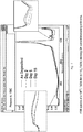
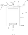
- FIG. 17 a schematic apparatus for performing the embodiments of the invention is generally illustrated at 10. It comprises a chamber 11, a showerhead 12, a waversupport 13 and respective high and low frequency sources 14 and 15.
- the showerhead 12 is arranged to receive two precursors (TEOS and O 2 ).
- Matching units 16 and 17 are provided for the high and low frequency sources 14 and 15 respectively and a pumped outlet 18 is provided for removing surplus reaction gases.
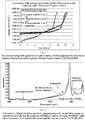
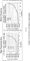
- Figure 2 illustrates at the relationship between no plasma treatment and plasma treatment on films deposited at 150°C and it is again seen that the breakdown characteristics are improved.
- Figure 3 similarly illustrates such characteristics in dependence on when the plasma treatment takes place and it would be seen that it is effective even after quite a lengthy vacuum break but that it seems to be advantageous to have a vacuum break at least up until 24 hours.
- Figure 4 shows the FTIR spectra for a number of films having different lengths of the plasma treatment.
- the plasma treatment removes OH peaks at ⁇ 3300 and 980CM -1 .
- There is also a very small peak at 2340CM -1 which indicates the presence of Si-H bonds on more near the surface of the film which would make the film hydrophobic and reduce absorption of water vapour on or through the surface of the film, which has relative little OH in its bulk.
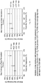
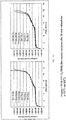
- Figures 5 and 6 illustrate the effect of different types of anneals and it would be observed that the H 2 plasma treatment is significantly better than preventing reabsorbtion.
- Figure 7 looks at the reabsorbtion over time.
- the H 2 plasma treatment reduces the moisture in the film and reduces the rate of reabsorbtion into the film, probably, at least in part, by creating a hydrophobic surface.
- the results are excellent even at a deposition temperature of 150°C. It is therefore likely that serviceable films can be obtained below this temperature.
- the treatment can be carried out after a vacuum break and they possibly be enhanced by such a break.
- the H 2 plasma treatment temperature is low, for example, 200°C or even lower, around 125°C or 150°C.
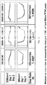
- Figures 8a and 8b show the step coverage against the temperature of the support of platen 13.
- the step coverage improves as temperature is increased and as the O 2 /TEOS ratio is increased.
- acceptable step coverage can be achieved at historically low temperatures.
- Figure 9 shows the effect of deposition temperature on the leakage current of a plasma treated film and it will be seen that the results are better at high temperature but with the plasma acceptable results can be achieved at quite low temperatures.
- Figure 10 illustrates the relationship of deposition rate to 0 2 /TEOS ratio and it would be seen that the deposition rate falls as the ratio is increased.
- the showerhead is preferably powered at mixed frequencies and a typical arrangement is a high frequency of 13.56MHz and a low frequency of 375kHz. It is however believed that the low frequency component could be increased in frequency at least up until 2MHz. It has been determined that the introduction of the low frequency component does not change the deposition rate and therefore is not believed to be increasing the density of the film by ion bombardment.
- Figure 11 shows the effect of introducing the low frequency component on reabsorbtion.
- the deposition conditions for this experiment were as set out in process 4 subject to the variation in the RF components indicated in the figure. There is visibly less reabsorbtion when mixed frequency is used as opposed to a single 13.56MHz RF source.
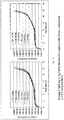
- Figure 12 compares the difference in leakage current between high frequency only and mixed frequency.
- the references to dot1, dot2, and dot3 indicate measurements at different points on the waver. It will be seen that there is a significant improvement in the leakage characteristics. In general it can be concluded that the presence of the low frequency power provides less OH reabsorbtion and a higher breakdown voltage.
- Figures 14 to 16 effectively compare the electrical response after 24 hours reabsorbtion at 175°C and 200°C for different O 2 /TEOS ratios. It would be seen that at the low ratio of 6:1 there is significant reabsorbtion at 175°C but the extent of the deterioration and performance decreases when the ratio is increased.
- Figure 16 illustrates the good absorbtion performance of a process 2 film.
- films may be deposited at temperatures as low as 125°C.
Landscapes
- Chemical & Material Sciences (AREA)
- Engineering & Computer Science (AREA)
- Metallurgy (AREA)
- Chemical Kinetics & Catalysis (AREA)
- Materials Engineering (AREA)
- Mechanical Engineering (AREA)
- General Chemical & Material Sciences (AREA)
- Organic Chemistry (AREA)
- Physics & Mathematics (AREA)
- Plasma & Fusion (AREA)
- Inorganic Chemistry (AREA)
- Formation Of Insulating Films (AREA)
- Chemical Vapour Deposition (AREA)
- Internal Circuitry In Semiconductor Integrated Circuit Devices (AREA)
Claims (9)
- Procédé de dépôt d'un film de SiO2 diélectrique, inorganique, à des températures au-dessous de 250°C à l'aide d'un dépôt chimique en phase vapeur assisté par plasma (PECVD) dans une chambre comprenant l'introduction d'orthosilicate de tétraéthyle (TEOS) et d'un rapport O2/TEOS d'entre 15:1 et 25:1 ;
dans lequel les précurseurs sont déposés à l'aide d'une pomme d'arrosage commandée par RF, la pomme d'arrosage étant commandée à l'aide d'un composant haute fréquence et d'un composant basse fréquence ; et
le composant haute fréquence est à 13,56 MHz et le composant basse fréquence est 350 KHz-2 MHz. - Procédé selon la revendication 1, dans lequel la puissance fournie à la haute fréquence est approximativement de deux fois la puissance du composant basse fréquence.
- Procédé selon l'une des revendications 1 ou 2, comprenant en outre la réalisation d'un traitement par plasma de H2 sur le film tel que déposé.
- Procédé selon la revendication 3, dans lequel le traitement par plasma de H2 est effectué après un cassage de vide.
- Procédé selon la revendication 3 ou la revendication 4, dans lequel le traitement par plasma de H2 forme ou reforme des liaisons Si-H sur la surface du film.
- Procédé selon l'une quelconque des revendications précédentes, dans lequel le film est déposé à des températures se situant dans la plage de 150°C-200°C.
- Procédé selon la revendication 3 ou selon l'une quelconque des revendications 4 à 6 en tant que dépendante de la revendication 3, dans lequel une simple fréquence RF est utilisée pour le plasma de H2.
- Procédé selon la revendication 7, dans lequel la simple fréquence RF est 13,56 MHz.
- Procédé selon la revendication 3 ou selon l'une quelconque des revendications 4 à 8 en tant que dépendante de la revendication 3, dans lequel la température de plasma de H2 se situe dans la plage de 125°C à 200°C.
Applications Claiming Priority (1)
| Application Number | Priority Date | Filing Date | Title |
|---|---|---|---|
| GBGB0922647.3A GB0922647D0 (en) | 2009-12-24 | 2009-12-24 | Methods of depositing SiO² films |
Publications (3)
| Publication Number | Publication Date |
|---|---|
| EP2362003A2 EP2362003A2 (fr) | 2011-08-31 |
| EP2362003A3 EP2362003A3 (fr) | 2011-09-07 |
| EP2362003B1 true EP2362003B1 (fr) | 2017-07-05 |
Family
ID=41716978
Family Applications (1)
| Application Number | Title | Priority Date | Filing Date |
|---|---|---|---|
| EP10275131.0A Active EP2362003B1 (fr) | 2009-12-24 | 2010-12-20 | Procédé pour déposer des films de SiO2 |
Country Status (6)
| Country | Link |
|---|---|
| EP (1) | EP2362003B1 (fr) |
| JP (1) | JP6058876B2 (fr) |
| KR (1) | KR101472733B1 (fr) |
| CN (1) | CN102108497B (fr) |
| GB (1) | GB0922647D0 (fr) |
| TW (1) | TWI518201B (fr) |
Families Citing this family (14)
| Publication number | Priority date | Publication date | Assignee | Title |
|---|---|---|---|---|
| US8329575B2 (en) * | 2010-12-22 | 2012-12-11 | Applied Materials, Inc. | Fabrication of through-silicon vias on silicon wafers |
| GB201207448D0 (en) | 2012-04-26 | 2012-06-13 | Spts Technologies Ltd | Method of depositing silicon dioxide films |
| JP2015029004A (ja) * | 2013-07-30 | 2015-02-12 | 株式会社アルバック | プラズマcvd装置及び成膜方法 |
| GB201410317D0 (en) * | 2014-06-10 | 2014-07-23 | Spts Technologies Ltd | Substrate |
| US9390910B2 (en) * | 2014-10-03 | 2016-07-12 | Applied Materials, Inc. | Gas flow profile modulated control of overlay in plasma CVD films |
| WO2017051993A1 (fr) * | 2015-09-21 | 2017-03-30 | 주식회사 포스코 | Substrat soumis à traitement coloré et procédé de traitement coloré correspondant |
| KR101772772B1 (ko) * | 2015-12-08 | 2017-08-29 | 주식회사 포스코 | 표면 처리된 기판 및 이의 제조방법 |
| GB201522552D0 (en) * | 2015-12-21 | 2016-02-03 | Spts Technologies Ltd | Method of improving adhesion |
| CN106783535A (zh) * | 2016-11-28 | 2017-05-31 | 武汉新芯集成电路制造有限公司 | 一种改善peteos薄膜缺陷的方法和半导体结构 |
| CN108018538A (zh) * | 2017-11-24 | 2018-05-11 | 中航(重庆)微电子有限公司 | 采用pe-teos工艺制备二氧化硅薄膜的方法及设备 |
| CN111235547B (zh) * | 2020-04-27 | 2020-08-07 | 上海陛通半导体能源科技股份有限公司 | 化学气相沉积方法 |
| CN114000123A (zh) * | 2021-11-02 | 2022-02-01 | 浙江光特科技有限公司 | 一种制备SiO2薄膜的方法、芯片及装置 |
| KR102896684B1 (ko) * | 2022-12-16 | 2025-12-09 | 주식회사 원익아이피에스 | 실리콘 산화막 형성 방법 |
| CN116479405A (zh) * | 2023-06-08 | 2023-07-25 | 上海陛通半导体能源科技股份有限公司 | 一种12英寸超高均匀性非晶氧化硅薄膜的化学气相沉积方法 |
Family Cites Families (11)
| Publication number | Priority date | Publication date | Assignee | Title |
|---|---|---|---|---|
| US5356722A (en) * | 1992-06-10 | 1994-10-18 | Applied Materials, Inc. | Method for depositing ozone/TEOS silicon oxide films of reduced surface sensitivity |
| DE19523442A1 (de) * | 1995-06-28 | 1997-01-02 | Antec Angewandte Neue Technolo | Verfahren zur Beschichtung von Gegenständen aus Metall oder Metall-Legierungen oder entsprechenden Oberflächen |
| JP2973905B2 (ja) * | 1995-12-27 | 1999-11-08 | 日本電気株式会社 | 半導体装置の製造方法 |
| US6028014A (en) * | 1997-11-10 | 2000-02-22 | Lsi Logic Corporation | Plasma-enhanced oxide process optimization and material and apparatus therefor |
| JP3933793B2 (ja) * | 1998-06-16 | 2007-06-20 | 富士通株式会社 | シリコン酸化膜の形成方法及び薄膜磁気ヘッドの製造方法 |
| JP3248492B2 (ja) * | 1998-08-14 | 2002-01-21 | 日本電気株式会社 | 半導体装置及びその製造方法 |
| JP3184177B2 (ja) * | 1999-03-26 | 2001-07-09 | キヤノン販売株式会社 | 層間絶縁膜の形成方法、半導体製造装置、及び半導体装置 |
| US7247252B2 (en) * | 2002-06-20 | 2007-07-24 | Taiwan Semiconductor Manufacturing Co., Ltd. | Method of avoiding plasma arcing during RIE etching |
| JP2005150299A (ja) * | 2003-11-13 | 2005-06-09 | Seiko Epson Corp | 半導体チップ、半導体装置及び半導体装置の製造方法、回路基板及び電子機器 |
| US7888273B1 (en) * | 2006-11-01 | 2011-02-15 | Novellus Systems, Inc. | Density gradient-free gap fill |
| JP4985411B2 (ja) * | 2008-01-08 | 2012-07-25 | 住友電気工業株式会社 | 半導体光素子を作製する方法 |
-
2009
- 2009-12-24 GB GBGB0922647.3A patent/GB0922647D0/en not_active Ceased
-
2010
- 2010-12-20 EP EP10275131.0A patent/EP2362003B1/fr active Active
- 2010-12-20 TW TW099144743A patent/TWI518201B/zh active
- 2010-12-22 JP JP2010286580A patent/JP6058876B2/ja active Active
- 2010-12-24 CN CN201010615668.9A patent/CN102108497B/zh active Active
- 2010-12-24 KR KR1020100134279A patent/KR101472733B1/ko active Active
Non-Patent Citations (1)
| Title |
|---|
| None * |
Also Published As
| Publication number | Publication date |
|---|---|
| KR101472733B1 (ko) | 2014-12-15 |
| TW201139719A (en) | 2011-11-16 |
| EP2362003A3 (fr) | 2011-09-07 |
| CN102108497B (zh) | 2015-07-15 |
| CN102108497A (zh) | 2011-06-29 |
| GB0922647D0 (en) | 2010-02-10 |
| TWI518201B (zh) | 2016-01-21 |
| JP2011135084A (ja) | 2011-07-07 |
| JP6058876B2 (ja) | 2017-01-11 |
| KR20110074478A (ko) | 2011-06-30 |
| EP2362003A2 (fr) | 2011-08-31 |
Similar Documents
| Publication | Publication Date | Title |
|---|---|---|
| EP2362003B1 (fr) | Procédé pour déposer des films de SiO2 | |
| US7989365B2 (en) | Remote plasma source seasoning | |
| EP0953066B1 (fr) | Procédé pour remplissage d'espaces avec DEPOT CHIMIQUE EN PHASE VAPEUR ACTIVE PAR PLASMA INDUCTIF | |
| US8647722B2 (en) | Method of forming insulation film using plasma treatment cycles | |
| US9165762B2 (en) | Method of depositing silicone dioxide films | |
| US8889566B2 (en) | Low cost flowable dielectric films | |
| EP1482070B1 (fr) | Additifs pour l'amélioration de la stabilité mécanique des films à constante diélectrique faible | |
| US9018108B2 (en) | Low shrinkage dielectric films | |
| US7951683B1 (en) | In-situ process layer using silicon-rich-oxide for etch selectivity in high AR gapfill | |
| US20140186544A1 (en) | Metal processing using high density plasma | |
| CN111910175A (zh) | 用于重整非晶碳聚合物膜的方法 | |
| US20130288485A1 (en) | Densification for flowable films | |
| WO2006078719A2 (fr) | Traitement d'interface pour l'amelioration d'adhesion entre des empilements a faibles constante dielectrique | |
| WO2001001472A1 (fr) | Procede et appareil permettant de former un film sur un substrat | |
| KR20190130044A (ko) | 원격 질소 라디칼 소스에 의해 가능하게 되는 높은 증착률의 고품질 실리콘 질화물 | |
| US20110318502A1 (en) | Methods of depositing sio2 films | |
| EP2045357A1 (fr) | Procédé de formation de films de nitrure en silicone | |
| CN105765705B (zh) | 氮化硅膜及其制造方法与其制造装置 | |
| US20060105581A1 (en) | Glycol doping agents in carbon doped oxide films | |
| EP3922750A2 (fr) | Procédé de dépôt | |
| US7335584B2 (en) | Method of using SACVD deposition and corresponding deposition reactor | |
| WO2012177716A2 (fr) | Dépôt d'un film de métal de type n à l'aide d'une couche d'initiation | |
| US20010018275A1 (en) | Method of using SACVD deposition and corresponding deposition reactor | |
| JP2012190831A (ja) | 半導体装置の製造方法および半導体装置 |
Legal Events
| Date | Code | Title | Description |
|---|---|---|---|
| PUAI | Public reference made under article 153(3) epc to a published international application that has entered the european phase |
Free format text: ORIGINAL CODE: 0009012 |
|
| PUAL | Search report despatched |
Free format text: ORIGINAL CODE: 0009013 |
|
| AK | Designated contracting states |
Kind code of ref document: A2 Designated state(s): AL AT BE BG CH CY CZ DE DK EE ES FI FR GB GR HR HU IE IS IT LI LT LU LV MC MK MT NL NO PL PT RO RS SE SI SK SM TR |
|
| AX | Request for extension of the european patent |
Extension state: BA ME |
|
| AK | Designated contracting states |
Kind code of ref document: A3 Designated state(s): AL AT BE BG CH CY CZ DE DK EE ES FI FR GB GR HR HU IE IS IT LI LT LU LV MC MK MT NL NO PL PT RO RS SE SI SK SM TR |
|
| AX | Request for extension of the european patent |
Extension state: BA ME |
|
| RIC1 | Information provided on ipc code assigned before grant |
Ipc: C23C 16/52 20060101ALI20110802BHEP Ipc: C23C 16/50 20060101ALI20110802BHEP Ipc: C23C 16/505 20060101ALI20110802BHEP Ipc: C23C 16/56 20060101ALI20110802BHEP Ipc: C23C 16/40 20060101AFI20110802BHEP Ipc: C23C 16/455 20060101ALI20110802BHEP |
|
| 17P | Request for examination filed |
Effective date: 20120305 |
|
| 111Z | Information provided on other rights and legal means of execution |
Free format text: AL AT BE BG CH CY CZ DE DK EE ES FI FR GB GR HR HU IE IS IT LT LU LV MC MK MT NL NO PL PT RO RS SE SI SK SM TR Effective date: 20150702 |
|
| 17Q | First examination report despatched |
Effective date: 20151008 |
|
| D11X | Information provided on other rights and legal means of execution (deleted) | ||
| GRAP | Despatch of communication of intention to grant a patent |
Free format text: ORIGINAL CODE: EPIDOSNIGR1 |
|
| STAA | Information on the status of an ep patent application or granted ep patent |
Free format text: STATUS: GRANT OF PATENT IS INTENDED |
|
| INTG | Intention to grant announced |
Effective date: 20161207 |
|
| RIN1 | Information on inventor provided before grant (corrected) |
Inventor name: BURGESS, STEPHEN ROBERT Inventor name: ARCHARD, DANIEL THOMAS Inventor name: GILES, KATHERINE Inventor name: PRICE, ANDREW |
|
| GRAJ | Information related to disapproval of communication of intention to grant by the applicant or resumption of examination proceedings by the epo deleted |
Free format text: ORIGINAL CODE: EPIDOSDIGR1 |
|
| GRAP | Despatch of communication of intention to grant a patent |
Free format text: ORIGINAL CODE: EPIDOSNIGR1 |
|
| INTG | Intention to grant announced |
Effective date: 20170126 |
|
| INTG | Intention to grant announced |
Effective date: 20170207 |
|
| GRAS | Grant fee paid |
Free format text: ORIGINAL CODE: EPIDOSNIGR3 |
|
| GRAA | (expected) grant |
Free format text: ORIGINAL CODE: 0009210 |
|
| STAA | Information on the status of an ep patent application or granted ep patent |
Free format text: STATUS: THE PATENT HAS BEEN GRANTED |
|
| AK | Designated contracting states |
Kind code of ref document: B1 Designated state(s): AL AT BE BG CH CY CZ DE DK EE ES FI FR GB GR HR HU IE IS IT LI LT LU LV MC MK MT NL NO PL PT RO RS SE SI SK SM TR |
|
| REG | Reference to a national code |
Ref country code: GB Ref legal event code: FG4D |
|
| REG | Reference to a national code |
Ref country code: CH Ref legal event code: EP |
|
| REG | Reference to a national code |
Ref country code: AT Ref legal event code: REF Ref document number: 906669 Country of ref document: AT Kind code of ref document: T Effective date: 20170715 |
|
| REG | Reference to a national code |
Ref country code: IE Ref legal event code: FG4D |
|
| REG | Reference to a national code |
Ref country code: DE Ref legal event code: R096 Ref document number: 602010043407 Country of ref document: DE |
|
| REG | Reference to a national code |
Ref country code: NL Ref legal event code: MP Effective date: 20170705 |
|
| REG | Reference to a national code |
Ref country code: AT Ref legal event code: MK05 Ref document number: 906669 Country of ref document: AT Kind code of ref document: T Effective date: 20170705 |
|
| REG | Reference to a national code |
Ref country code: LT Ref legal event code: MG4D |
|
| REG | Reference to a national code |
Ref country code: FR Ref legal event code: PLFP Year of fee payment: 8 |
|
| PG25 | Lapsed in a contracting state [announced via postgrant information from national office to epo] |
Ref country code: NL Free format text: LAPSE BECAUSE OF FAILURE TO SUBMIT A TRANSLATION OF THE DESCRIPTION OR TO PAY THE FEE WITHIN THE PRESCRIBED TIME-LIMIT Effective date: 20170705 Ref country code: SE Free format text: LAPSE BECAUSE OF FAILURE TO SUBMIT A TRANSLATION OF THE DESCRIPTION OR TO PAY THE FEE WITHIN THE PRESCRIBED TIME-LIMIT Effective date: 20170705 Ref country code: HR Free format text: LAPSE BECAUSE OF FAILURE TO SUBMIT A TRANSLATION OF THE DESCRIPTION OR TO PAY THE FEE WITHIN THE PRESCRIBED TIME-LIMIT Effective date: 20170705 Ref country code: FI Free format text: LAPSE BECAUSE OF FAILURE TO SUBMIT A TRANSLATION OF THE DESCRIPTION OR TO PAY THE FEE WITHIN THE PRESCRIBED TIME-LIMIT Effective date: 20170705 Ref country code: AT Free format text: LAPSE BECAUSE OF FAILURE TO SUBMIT A TRANSLATION OF THE DESCRIPTION OR TO PAY THE FEE WITHIN THE PRESCRIBED TIME-LIMIT Effective date: 20170705 Ref country code: NO Free format text: LAPSE BECAUSE OF FAILURE TO SUBMIT A TRANSLATION OF THE DESCRIPTION OR TO PAY THE FEE WITHIN THE PRESCRIBED TIME-LIMIT Effective date: 20171005 Ref country code: LT Free format text: LAPSE BECAUSE OF FAILURE TO SUBMIT A TRANSLATION OF THE DESCRIPTION OR TO PAY THE FEE WITHIN THE PRESCRIBED TIME-LIMIT Effective date: 20170705 |
|
| PG25 | Lapsed in a contracting state [announced via postgrant information from national office to epo] |
Ref country code: PL Free format text: LAPSE BECAUSE OF FAILURE TO SUBMIT A TRANSLATION OF THE DESCRIPTION OR TO PAY THE FEE WITHIN THE PRESCRIBED TIME-LIMIT Effective date: 20170705 Ref country code: IS Free format text: LAPSE BECAUSE OF FAILURE TO SUBMIT A TRANSLATION OF THE DESCRIPTION OR TO PAY THE FEE WITHIN THE PRESCRIBED TIME-LIMIT Effective date: 20171105 Ref country code: GR Free format text: LAPSE BECAUSE OF FAILURE TO SUBMIT A TRANSLATION OF THE DESCRIPTION OR TO PAY THE FEE WITHIN THE PRESCRIBED TIME-LIMIT Effective date: 20171006 Ref country code: RS Free format text: LAPSE BECAUSE OF FAILURE TO SUBMIT A TRANSLATION OF THE DESCRIPTION OR TO PAY THE FEE WITHIN THE PRESCRIBED TIME-LIMIT Effective date: 20170705 Ref country code: BG Free format text: LAPSE BECAUSE OF FAILURE TO SUBMIT A TRANSLATION OF THE DESCRIPTION OR TO PAY THE FEE WITHIN THE PRESCRIBED TIME-LIMIT Effective date: 20171005 Ref country code: LV Free format text: LAPSE BECAUSE OF FAILURE TO SUBMIT A TRANSLATION OF THE DESCRIPTION OR TO PAY THE FEE WITHIN THE PRESCRIBED TIME-LIMIT Effective date: 20170705 Ref country code: ES Free format text: LAPSE BECAUSE OF FAILURE TO SUBMIT A TRANSLATION OF THE DESCRIPTION OR TO PAY THE FEE WITHIN THE PRESCRIBED TIME-LIMIT Effective date: 20170705 |
|
| REG | Reference to a national code |
Ref country code: DE Ref legal event code: R097 Ref document number: 602010043407 Country of ref document: DE |
|
| PG25 | Lapsed in a contracting state [announced via postgrant information from national office to epo] |
Ref country code: DK Free format text: LAPSE BECAUSE OF FAILURE TO SUBMIT A TRANSLATION OF THE DESCRIPTION OR TO PAY THE FEE WITHIN THE PRESCRIBED TIME-LIMIT Effective date: 20170705 Ref country code: CZ Free format text: LAPSE BECAUSE OF FAILURE TO SUBMIT A TRANSLATION OF THE DESCRIPTION OR TO PAY THE FEE WITHIN THE PRESCRIBED TIME-LIMIT Effective date: 20170705 Ref country code: RO Free format text: LAPSE BECAUSE OF FAILURE TO SUBMIT A TRANSLATION OF THE DESCRIPTION OR TO PAY THE FEE WITHIN THE PRESCRIBED TIME-LIMIT Effective date: 20170705 |
|
| PLBE | No opposition filed within time limit |
Free format text: ORIGINAL CODE: 0009261 |
|
| STAA | Information on the status of an ep patent application or granted ep patent |
Free format text: STATUS: NO OPPOSITION FILED WITHIN TIME LIMIT |
|
| PG25 | Lapsed in a contracting state [announced via postgrant information from national office to epo] |
Ref country code: SM Free format text: LAPSE BECAUSE OF FAILURE TO SUBMIT A TRANSLATION OF THE DESCRIPTION OR TO PAY THE FEE WITHIN THE PRESCRIBED TIME-LIMIT Effective date: 20170705 Ref country code: EE Free format text: LAPSE BECAUSE OF FAILURE TO SUBMIT A TRANSLATION OF THE DESCRIPTION OR TO PAY THE FEE WITHIN THE PRESCRIBED TIME-LIMIT Effective date: 20170705 Ref country code: IT Free format text: LAPSE BECAUSE OF FAILURE TO SUBMIT A TRANSLATION OF THE DESCRIPTION OR TO PAY THE FEE WITHIN THE PRESCRIBED TIME-LIMIT Effective date: 20170705 Ref country code: SK Free format text: LAPSE BECAUSE OF FAILURE TO SUBMIT A TRANSLATION OF THE DESCRIPTION OR TO PAY THE FEE WITHIN THE PRESCRIBED TIME-LIMIT Effective date: 20170705 |
|
| 26N | No opposition filed |
Effective date: 20180406 |
|
| REG | Reference to a national code |
Ref country code: CH Ref legal event code: PL |
|
| PG25 | Lapsed in a contracting state [announced via postgrant information from national office to epo] |
Ref country code: SI Free format text: LAPSE BECAUSE OF FAILURE TO SUBMIT A TRANSLATION OF THE DESCRIPTION OR TO PAY THE FEE WITHIN THE PRESCRIBED TIME-LIMIT Effective date: 20170705 |
|
| REG | Reference to a national code |
Ref country code: IE Ref legal event code: MM4A |
|
| PG25 | Lapsed in a contracting state [announced via postgrant information from national office to epo] |
Ref country code: MT Free format text: LAPSE BECAUSE OF NON-PAYMENT OF DUE FEES Effective date: 20171220 Ref country code: LU Free format text: LAPSE BECAUSE OF NON-PAYMENT OF DUE FEES Effective date: 20171220 |
|
| REG | Reference to a national code |
Ref country code: BE Ref legal event code: MM Effective date: 20171231 |
|
| PG25 | Lapsed in a contracting state [announced via postgrant information from national office to epo] |
Ref country code: IE Free format text: LAPSE BECAUSE OF NON-PAYMENT OF DUE FEES Effective date: 20171220 |
|
| PG25 | Lapsed in a contracting state [announced via postgrant information from national office to epo] |
Ref country code: LI Free format text: LAPSE BECAUSE OF NON-PAYMENT OF DUE FEES Effective date: 20171231 Ref country code: BE Free format text: LAPSE BECAUSE OF NON-PAYMENT OF DUE FEES Effective date: 20171231 Ref country code: CH Free format text: LAPSE BECAUSE OF NON-PAYMENT OF DUE FEES Effective date: 20171231 |
|
| PG25 | Lapsed in a contracting state [announced via postgrant information from national office to epo] |
Ref country code: MC Free format text: LAPSE BECAUSE OF FAILURE TO SUBMIT A TRANSLATION OF THE DESCRIPTION OR TO PAY THE FEE WITHIN THE PRESCRIBED TIME-LIMIT Effective date: 20170705 Ref country code: HU Free format text: LAPSE BECAUSE OF FAILURE TO SUBMIT A TRANSLATION OF THE DESCRIPTION OR TO PAY THE FEE WITHIN THE PRESCRIBED TIME-LIMIT; INVALID AB INITIO Effective date: 20101220 |
|
| PG25 | Lapsed in a contracting state [announced via postgrant information from national office to epo] |
Ref country code: CY Free format text: LAPSE BECAUSE OF NON-PAYMENT OF DUE FEES Effective date: 20170705 |
|
| PG25 | Lapsed in a contracting state [announced via postgrant information from national office to epo] |
Ref country code: MK Free format text: LAPSE BECAUSE OF FAILURE TO SUBMIT A TRANSLATION OF THE DESCRIPTION OR TO PAY THE FEE WITHIN THE PRESCRIBED TIME-LIMIT Effective date: 20170705 |
|
| PG25 | Lapsed in a contracting state [announced via postgrant information from national office to epo] |
Ref country code: TR Free format text: LAPSE BECAUSE OF FAILURE TO SUBMIT A TRANSLATION OF THE DESCRIPTION OR TO PAY THE FEE WITHIN THE PRESCRIBED TIME-LIMIT Effective date: 20170705 |
|
| PG25 | Lapsed in a contracting state [announced via postgrant information from national office to epo] |
Ref country code: PT Free format text: LAPSE BECAUSE OF FAILURE TO SUBMIT A TRANSLATION OF THE DESCRIPTION OR TO PAY THE FEE WITHIN THE PRESCRIBED TIME-LIMIT Effective date: 20170705 |
|
| PG25 | Lapsed in a contracting state [announced via postgrant information from national office to epo] |
Ref country code: AL Free format text: LAPSE BECAUSE OF FAILURE TO SUBMIT A TRANSLATION OF THE DESCRIPTION OR TO PAY THE FEE WITHIN THE PRESCRIBED TIME-LIMIT Effective date: 20170705 |
|
| REG | Reference to a national code |
Ref country code: DE Ref legal event code: R082 Ref document number: 602010043407 Country of ref document: DE Representative=s name: KANDLBINDER, MARKUS, DIPL.-PHYS., DE |
|
| PGFP | Annual fee paid to national office [announced via postgrant information from national office to epo] |
Ref country code: GB Payment date: 20251229 Year of fee payment: 16 |
|
| PGFP | Annual fee paid to national office [announced via postgrant information from national office to epo] |
Ref country code: FR Payment date: 20251226 Year of fee payment: 16 |
|
| PGFP | Annual fee paid to national office [announced via postgrant information from national office to epo] |
Ref country code: DE Payment date: 20251229 Year of fee payment: 16 |