EP2362374A2 - Antriebsschaltung mit visueller Verbesserung für LCD-Anzeige und Verfahren - Google Patents
Antriebsschaltung mit visueller Verbesserung für LCD-Anzeige und Verfahren Download PDFInfo
- Publication number
- EP2362374A2 EP2362374A2 EP10191779A EP10191779A EP2362374A2 EP 2362374 A2 EP2362374 A2 EP 2362374A2 EP 10191779 A EP10191779 A EP 10191779A EP 10191779 A EP10191779 A EP 10191779A EP 2362374 A2 EP2362374 A2 EP 2362374A2
- Authority
- EP
- European Patent Office
- Prior art keywords
- capacitor
- sub
- gate
- common voltage
- line signal
- Prior art date
- Legal status (The legal status is an assumption and is not a legal conclusion. Google has not performed a legal analysis and makes no representation as to the accuracy of the status listed.)
- Granted
Links
Images


Classifications
-
- G—PHYSICS
- G09—EDUCATION; CRYPTOGRAPHY; DISPLAY; ADVERTISING; SEALS
- G09G—ARRANGEMENTS OR CIRCUITS FOR CONTROL OF INDICATING DEVICES USING STATIC MEANS TO PRESENT VARIABLE INFORMATION
- G09G3/00—Control arrangements or circuits, of interest only in connection with visual indicators other than cathode-ray tubes
- G09G3/20—Control arrangements or circuits, of interest only in connection with visual indicators other than cathode-ray tubes for presentation of an assembly of a number of characters, e.g. a page, by composing the assembly by combination of individual elements arranged in a matrix no fixed position being assigned to or needed to be assigned to the individual characters or partial characters
- G09G3/34—Control arrangements or circuits, of interest only in connection with visual indicators other than cathode-ray tubes for presentation of an assembly of a number of characters, e.g. a page, by composing the assembly by combination of individual elements arranged in a matrix no fixed position being assigned to or needed to be assigned to the individual characters or partial characters by control of light from an independent source
- G09G3/36—Control arrangements or circuits, of interest only in connection with visual indicators other than cathode-ray tubes for presentation of an assembly of a number of characters, e.g. a page, by composing the assembly by combination of individual elements arranged in a matrix no fixed position being assigned to or needed to be assigned to the individual characters or partial characters by control of light from an independent source using liquid crystals
- G09G3/3611—Control of matrices with row and column drivers
- G09G3/3648—Control of matrices with row and column drivers using an active matrix
-
- G—PHYSICS
- G09—EDUCATION; CRYPTOGRAPHY; DISPLAY; ADVERTISING; SEALS
- G09G—ARRANGEMENTS OR CIRCUITS FOR CONTROL OF INDICATING DEVICES USING STATIC MEANS TO PRESENT VARIABLE INFORMATION
- G09G2300/00—Aspects of the constitution of display devices
- G09G2300/04—Structural and physical details of display devices
- G09G2300/0439—Pixel structures
- G09G2300/0443—Pixel structures with several sub-pixels for the same colour in a pixel, not specifically used to display gradations
-
- G—PHYSICS
- G09—EDUCATION; CRYPTOGRAPHY; DISPLAY; ADVERTISING; SEALS
- G09G—ARRANGEMENTS OR CIRCUITS FOR CONTROL OF INDICATING DEVICES USING STATIC MEANS TO PRESENT VARIABLE INFORMATION
- G09G2300/00—Aspects of the constitution of display devices
- G09G2300/04—Structural and physical details of display devices
- G09G2300/0439—Pixel structures
- G09G2300/0443—Pixel structures with several sub-pixels for the same colour in a pixel, not specifically used to display gradations
- G09G2300/0447—Pixel structures with several sub-pixels for the same colour in a pixel, not specifically used to display gradations for multi-domain technique to improve the viewing angle in a liquid crystal display, such as multi-vertical alignment [MVA]
-
- G—PHYSICS
- G09—EDUCATION; CRYPTOGRAPHY; DISPLAY; ADVERTISING; SEALS
- G09G—ARRANGEMENTS OR CIRCUITS FOR CONTROL OF INDICATING DEVICES USING STATIC MEANS TO PRESENT VARIABLE INFORMATION
- G09G2300/00—Aspects of the constitution of display devices
- G09G2300/08—Active matrix structure, i.e. with use of active elements, inclusive of non-linear two terminal elements, in the pixels together with light emitting or modulating elements
- G09G2300/0809—Several active elements per pixel in active matrix panels
- G09G2300/0814—Several active elements per pixel in active matrix panels used for selection purposes, e.g. logical AND for partial update
-
- G—PHYSICS
- G09—EDUCATION; CRYPTOGRAPHY; DISPLAY; ADVERTISING; SEALS
- G09G—ARRANGEMENTS OR CIRCUITS FOR CONTROL OF INDICATING DEVICES USING STATIC MEANS TO PRESENT VARIABLE INFORMATION
- G09G2300/00—Aspects of the constitution of display devices
- G09G2300/08—Active matrix structure, i.e. with use of active elements, inclusive of non-linear two terminal elements, in the pixels together with light emitting or modulating elements
- G09G2300/0809—Several active elements per pixel in active matrix panels
- G09G2300/0842—Several active elements per pixel in active matrix panels forming a memory circuit, e.g. a dynamic memory with one capacitor
- G09G2300/0852—Several active elements per pixel in active matrix panels forming a memory circuit, e.g. a dynamic memory with one capacitor being a dynamic memory with more than one capacitor
-
- G—PHYSICS
- G09—EDUCATION; CRYPTOGRAPHY; DISPLAY; ADVERTISING; SEALS
- G09G—ARRANGEMENTS OR CIRCUITS FOR CONTROL OF INDICATING DEVICES USING STATIC MEANS TO PRESENT VARIABLE INFORMATION
- G09G2300/00—Aspects of the constitution of display devices
- G09G2300/08—Active matrix structure, i.e. with use of active elements, inclusive of non-linear two terminal elements, in the pixels together with light emitting or modulating elements
- G09G2300/0876—Supplementary capacities in pixels having special driving circuits and electrodes instead of being connected to common electrode or ground; Use of additional capacitively coupled compensation electrodes
-
- G—PHYSICS
- G09—EDUCATION; CRYPTOGRAPHY; DISPLAY; ADVERTISING; SEALS
- G09G—ARRANGEMENTS OR CIRCUITS FOR CONTROL OF INDICATING DEVICES USING STATIC MEANS TO PRESENT VARIABLE INFORMATION
- G09G2310/00—Command of the display device
- G09G2310/02—Addressing, scanning or driving the display screen or processing steps related thereto
- G09G2310/0243—Details of the generation of driving signals
- G09G2310/0251—Precharge or discharge of pixel before applying new pixel voltage
-
- G—PHYSICS
- G09—EDUCATION; CRYPTOGRAPHY; DISPLAY; ADVERTISING; SEALS
- G09G—ARRANGEMENTS OR CIRCUITS FOR CONTROL OF INDICATING DEVICES USING STATIC MEANS TO PRESENT VARIABLE INFORMATION
- G09G2320/00—Control of display operating conditions
- G09G2320/02—Improving the quality of display appearance
- G09G2320/0242—Compensation of deficiencies in the appearance of colours
-
- G—PHYSICS
- G09—EDUCATION; CRYPTOGRAPHY; DISPLAY; ADVERTISING; SEALS
- G09G—ARRANGEMENTS OR CIRCUITS FOR CONTROL OF INDICATING DEVICES USING STATIC MEANS TO PRESENT VARIABLE INFORMATION
- G09G2320/00—Control of display operating conditions
- G09G2320/02—Improving the quality of display appearance
- G09G2320/028—Improving the quality of display appearance by changing the viewing angle properties, e.g. widening the viewing angle, adapting the viewing angle to the view direction
Definitions
- the present invention relates generally to a liquid crystal display (LCD) display and, more particularly, to a method for driving the pixels in an LCD display.
- LCD liquid crystal display
- a typical liquid crystal display (LCD) panel has a plurality of pixels arranged in a two-dimensional array, driven by a data driver and a gate driver.
- the LCD pixels 10 in a LCD panel 1 are arranged in rows and columns in a display area 100.
- a data driver 200 is used to provide a signal indicative of data to each of the columns and a gate driver is used to provide a gate line signal to each of the rows.
- a gate driver is used to provide a gate line signal to each of the rows.
- an image is generally presented in three colors: red (R), green (G) and blue (B).
- Each of the pixels 10 is typically divided into three color sub-pixels: red sub-pixel 20R, green sub-pixel 20G and blue sub-pixel 20B, as shown in Figure 2 .
- a data line 221 is used to provide the data signal to the R sub-pixel in a column
- a data line 222 is used to provide the data signal to the G sub-pixel in the same pixel column
- a data line 223 is used to provide the data signal to the B sub-pixel in the same pixel column.
- the data line 224 is used to provide the data signal to the R sub-pixel in the next pixel column.
- a gate line 231 is used to provide the gate line signal to all sub-pixels in a row and a gate line 232 is used to provide the gate line signal to all sub-pixels in the next row.
- each of the color sub-pixels may be further divided into a transmissive area and a reflective area.
- a typical LCD panel is fabricated with two substrates. As shown in Figure 3 , the LCD panel has an upper substrate 12 and a lower substrate 18 and a liquid crystal layer disposed between the substrates. On the upper substrate 12, a transparent, electrically conducting layer 14 is provided as a common electrode. In each of the color sub-pixels 20, an electrically conducting layer is disposed on the lower substrate 18 as a pixel electrode.
- the LCD panel also comprises an electronic component layer 17 for controlling the voltage between the common electrode and the pixel electrode.
- the common electrode is usually connected to a common ground or a common voltage source COM.
- a pixel in a liquid crystal display panel comprises a first sub-pixel area having a first sub-pixel electrode (32) and a second sub-pixel area having a second sub-pixel electrode (34).
- Each sub-pixel electrode is associated with a capacitor.
- the voltage level on the first sub-pixel electrode is substantially equal to or slightly higher than the voltage level on the second sub-pixel electrode and the capacitor associated with each sub-pixel electrode is charged.
- a circuit element causes the capacitor associated with the second sub-pixel electrode to transfer its charge to another capacitor, resulting in a reduction of the voltage level on the second sub-pixel electrode.
- the alignment of the liquid crystal molecules in the first sub-pixel area is slightly different from the alignment of the liquid crystal molecules in the second sub-pixel area, resulting in a slight brightness difference between the first and the second sub-pixel areas.
- This brightness difference may reduce the color shift of the liquid crystal display panel.
- the first aspect of the present invention is a liquid crystal display panel, comprising:
- one end of the first and second capacitors is connected to a common voltage (COM), and the circuit element comprises a fourth switching element (138) having a control end arranged to receive a second gate-line signal for connecting the second end of the third capacitor (CstB) to the common voltage after the first gate-line signal has passed.
- COM common voltage
- the circuit element comprises a fourth switching element (138) having a control end arranged to receive a second gate-line signal for connecting the second end of the third capacitor (CstB) to the common voltage after the first gate-line signal has passed.
- one end of the first and second capacitors is connected to a common voltage (COM), and the second end of the third capacitor (CstB) is also connected to the common voltage via a fourth capacitor (Cx).
- COM common voltage
- CstB third capacitor
- the second capacitor (ClcB) is connected to a fifth capacitor (CstB) in parallel.
- one end of the first and second capacitors is connected to a common voltage (COM), and the circuit element comprises a resistor (R) connected to the common voltage.
- COM common voltage
- R resistor
- the circuit element comprises a TFT with a diode connection.
- one end of the first and second capacitors is connected to a common voltage (COM), and the circuit element comprises a sixth capacitor (Cs) connected to the common voltage via a fourth switching element (138) having a control end arranged to receive a second gate-line signal for connecting the second end of the third capacitor (CstB) to the common voltage via the sixth capacitor (Cs) after the first gate-line signal has partially passed.
- COM common voltage
- the circuit element comprises a sixth capacitor (Cs) connected to the common voltage via a fourth switching element (138) having a control end arranged to receive a second gate-line signal for connecting the second end of the third capacitor (CstB) to the common voltage via the sixth capacitor (Cs) after the first gate-line signal has partially passed.
- one end of the first and second capacitors is connected to a common voltage (COM)
- the second end of the third capacitor (CstB) is connected to the third switching element (136) via a sixth capacitor (Cs)
- the circuit element comprises a fourth switching element (138) having a control end arranged to receive a second gate-line signal for connecting the second end of the third capacitor (CstB) to the common voltage after the first gate-line signal has partially passed.
- the second aspect of the present invention is a method for charge sharing in a liquid crystal display panel, the display panel comprising:
- the method comprises the steps of:
- one end of the first and second capacitors is connected to a common voltage (COM), and the circuit element comprises a fourth switching element (138) having a control end arranged to receive a second gate-line signal for connecting the second end of the third capacitor (CstB) to the common voltage after the first gate-line signal has passed.
- COM common voltage
- the circuit element comprises a fourth switching element (138) having a control end arranged to receive a second gate-line signal for connecting the second end of the third capacitor (CstB) to the common voltage after the first gate-line signal has passed.
- the method further comprises:
- the method further comprises:
- one end of the first and second capacitors is connected to a common voltage (COM), and the circuit element comprises a resistor (R) connected to the common voltage.
- COM common voltage
- R resistor
- one end of the first and second capacitors is connected to a common voltage (COM), and the circuit element comprises a sixth capacitor (Cs) connected to the common voltage via a fourth switching element (138) having a control end arranged to receive a second gate-line signal for connecting the second end of the third capacitor (CstB) to the common voltage via the sixth capacitor (Cs) after the first gate-line signal has partially passed.
- COM common voltage
- the circuit element comprises a sixth capacitor (Cs) connected to the common voltage via a fourth switching element (138) having a control end arranged to receive a second gate-line signal for connecting the second end of the third capacitor (CstB) to the common voltage via the sixth capacitor (Cs) after the first gate-line signal has partially passed.
- one end of the first and second capacitors is connected to a common voltage (COM)
- the second end of the third capacitor (CstB) is connected to the third switching element (136) via a sixth capacitor (Cs)
- the circuit element comprises a fourth switching element (138) having a control end arranged to receive a second gate-line signal for connecting the second end of the third capacitor (CstB) to the common voltage after the first gate-line signal has partially passed.
- a pixel or color sub-pixel of a liquid crystal display (LCD) panel comprises two areas, each area comprising an area electrode, together with a common electrode, for controlling the alignment of the liquid crystal layer in the respective area.
- the term sub-pixel will be used to represent a pixel or a color sub-pixel.
- the sub-pixel 20 1 includes a first sub-pixel electrode 32 1 to define a first sub-pixel area and a second sub-pixel electrode 34 1 to define a second sub-pixel area.
- the sub-pixel 20 2 includes a first sub-pixel electrode 32 2 to define a first sub-pixel area and a second sub-pixel electrode 34 2 to define a second sub-pixel area.
- the sub-pixel 20 3 and other sub-pixels may have similar first and second sub-pixel electrodes.
- the sub-pixels in a column share a data line
- the sub-pixels in a row share a gate line.
- the sub-pixels 20 1 , 20 2 , 20 3 , ... share a data line D1
- the sub-pixels in the next column (not shown) share a different data line D2.
- the sub-pixel 20 1 and other sub-pixels on the same row share a gate line G1; the sub-pixel 20 2 and other sub-pixels on the same row share a gate line G2; and the sub-pixel 20 3 and other sub-pixels on the same row share a gate line G3.
- the first sub-pixel electrode 32 1 of the sub-pixel 20 1 is connected to the data line D1 through a first switching element 132 1 and the second sub-pixel electrode 34 1 is connected to the data line D1 through a second switching element 134 1 .
- the control end of the first and second switching elements 132 1 and 134 1 is connected to the gate line G1.
- the first sub-pixel electrode 32 2 of the sub-pixel 20 2 is connected to the data line D1 through a first switching element 132 2 and the second sub-pixel electrode 34 2 is connected to the data line D1 through a second switching element 134 2 .
- the control end of the first and second switching elements 132 2 and 134 2 is connected to the gate line G2.
- the first sub-pixel electrode 32 1 and the common electrode form a capacitor ClcA and the second sub-pixel electrode 34 1 and the common electrode form a capacitor ClcB, as shown in Figure 5 .
- the first sub-pixel electrode 32 1 is connected to a storage capacitor CstA and the second sub-pixel electrode 34 1 is connected to a storage capacitor CstB.
- the first sub-pixel electrode 32 2 and the common electrode form a capacitor ClcA and the second sub-pixel electrode 34 2 and the common electrode form a capacitor ClcB.
- the first sub-pixel electrode 32 2 is connected to a storage capacitor CstA and the second sub-pixel electrode 34 2 is connected to a storage capacitor CstB.
- the charge storage capacitor CstB is also connected to the data line D1 via a third switching element 136 1 .
- the control end of the third switching element 136 1 is also connected to the gate line G1.
- the voltage level Va on the first sub-pixel electrode, the voltage level Vb on the second sub-pixel electrode and the voltage level Vx are substantially the same.
- the capacitors ClcA, CstB in the first sub-pixel area are charged according to the voltage level Va relative to COM.
- the capacitor ClcB in the second sub-pixel is charged according to the voltage level Vb relative to COM. Because the voltage level Vb on one end of the storage capacitor CstB and the voltage level Vx on the other end are substantially the same, the storage capacitor CstB is not charged.
- the second charge-storage capacitor CstB is connected to COM separately via a capacitor Cx and via a fourth switching element 138 1 which has a control end connected to a second gate-line G2 for discharging purposes, due to the change in the voltage level Vx between the second charge-storage capacitor CstB and capacitor Cx.
- Figure 6 is a timing chart showing the voltage level Va, the voltage level Vb and the voltage level Vx, in relation to the gate-line signals in G1 and G2.
- the voltage level Vb is reduced when the gate-line signal G2 is provided to the pixel.
- the amount of voltage reduction in Vb is determined by the charge amount transferred to the storage capacitor CstB.
- the gate-line signal G1 is provided to the sub-pixel 20 1 , all the first, second and third switching elements are in a conducting state.
- the equivalent circuit in this situation is illustrated in Figure 7a .
- the voltage levels Va, Vb and Vx is substantially equal to Vdata or the date signal on D1.
- Vx As the voltage level Vx has changed from Vdata to COM, some of the charge qB in ClcB is transferred to CstB.
- Va Vdata
- Va Vdata
- FIG 8 shows another embodiment of the present invention, wherein the capacitor Cx is omitted.
- the voltage levels Va and Vb are substantially the same as those shown in Figure 6 .
- the voltage level Vx may rise more rapidly as compared to that shown in Figure 6 .
- Figure 9 shows yet another embodiment of the present invention, which is a variation from the embodiment as shown in Figure 8 .
- a resistor R is used.
- the voltage level at point x is equal to COM, regardless of the gate-line signal G2.
- FIG 10 shows yet another embodiment of the present invention, which is a variation of the embodiment as shown in Figure 5 .
- a circuit element 139 1 is used.
- there is a current through the circuit element 139 1 when the gate-line signal G1 has passed, the current through the circuit element 139 1 is diminishing. Finally the voltage level at point x is equal to COM, regardless of the gate-line signal G2.
- the alignment of the liquid crystal molecules in the first sub-pixel area is slightly different from the alignment of the liquid crystal molecules in the second sub-pixel area, resulting in a slight brightness difference between the first and the second sub-pixel areas.
- This brightness difference may reduce the color shift of the liquid crystal display panel.
- the capacitor Cx is optional.
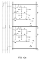
- Figure 11 shows a variation of the embodiment as shown in Figures 5 and 8 .
- the first sub-pixel area has a first sub-pixel electrode connected to a first storage capacitor CstA and the second sub-pixel area has a second sub-pixel electrode connected to a second storage capacitor CstB.
- the second sub-pixel electrode is connected to a circuit element 138 1 through a capacitor Cx.
- Va Vdata
- the gate-line signals G1 and G2 can be non-overlapping, as shown in Figure 6 .
- the gate-line signal Gm+1 partially occurs before the gate-line Gm has passed in order to pre-charge the pixels in the (m+1) th row. This requires the gate-line signals in adjacent gate-lines to be partially over-lapped, as shown in Figure 13 .
- the embodiments as shown in Figure 9 and 10 can be used when the gate-lines signals have an over-lapped period.
- a capacitor Cx is used to separate point x from the switching element 136 i when the gate-lines signals have an overlapped period.
- Figure 12 shows one of the different embodiments that can be used pre-charging purposes. As shown in Figure 12 , the switching element 136 i is connected to the circuit element 138 i through a capacitor Cx. The timing chart illustrating various voltage levels is shown in Figure 13 .
- each pixel has a first sub-pixel area comprising a first sub-pixel electrode electrically connected to a first capacitor (ClcA, CstA), the first sub-pixel electrode (where Va is) arranged to receive the data signal (G1) from one of the data lines via a first switching element (132); and a second sub-pixel area comprises a second sub-pixel electrode (where Vb is) electrically connected to a second capacitor and a first end of a third capacitor.
- the second capacitor is ClcB and the third capacitor is CstB.
- the second capacitor includes ClcB and CstB and the third capacitor is Cx.
- the second sub-pixel electrode arranged to receive said data signal from the same data line via a second switching element (134), wherein a second end of the third capacitor is connected to the same data line via a third switching element (136), wherein each of the first, second and third switching elements comprises a control end (gate terminal) arranged to receive a gate-line signal (G1) for charging the first capacitor and the second capacitor, and wherein the second end of the third capacitor is connected to a circuit element (138, R, 139) such that when the gate-line signal has at least partially passed, the circuit element causes part of electrical charge on the second capacitor to transfer to the third capacitor.
- the circuit element may have a a fourth switching element (138) arranged to receive a second gate-line signal (G2) for connecting the second end of the third capacitor to the common voltage after the first gate-line signal has passed.
- the present invention provide a method to achieve a voltage difference between the first sub-pixel electrode and the second sub-pixel electrode in some time periods during the operation of the liquid crystal display panel.
- the method includes the steps of connecting a first end of a third capacitor to the second sub-pixel electrode and a second end of the third capacitor to said one of the data lines via a third switching element, wherein each of the first, second and third switching elements comprises a control end arranged to receive a first gate line signal for switching; charging the first capacitor to a first voltage level through the first switching element and charging the second capacitor to a second voltage level through the second switching element in response to the first gate-line signal; and operatively connecting the second end of the third capacitor to a circuit element for transferring part of electrical charge on the second capacitor to the third capacitor when the first gate-line signal has at least partially passed so as to reduce the second voltage level.
Landscapes
- Engineering & Computer Science (AREA)
- Chemical & Material Sciences (AREA)
- Crystallography & Structural Chemistry (AREA)
- Physics & Mathematics (AREA)
- Computer Hardware Design (AREA)
- General Physics & Mathematics (AREA)
- Theoretical Computer Science (AREA)
- Liquid Crystal (AREA)
- Liquid Crystal Display Device Control (AREA)
- Control Of Indicators Other Than Cathode Ray Tubes (AREA)
Applications Claiming Priority (1)
| Application Number | Priority Date | Filing Date | Title |
|---|---|---|---|
| US12/660,315 US8411007B2 (en) | 2010-02-23 | 2010-02-23 | LCD display visual enhancement driving circuit and method |
Publications (3)
| Publication Number | Publication Date |
|---|---|
| EP2362374A2 true EP2362374A2 (de) | 2011-08-31 |
| EP2362374A3 EP2362374A3 (de) | 2012-05-02 |
| EP2362374B1 EP2362374B1 (de) | 2015-06-24 |
Family
ID=44070018
Family Applications (1)
| Application Number | Title | Priority Date | Filing Date |
|---|---|---|---|
| EP10191779.7A Active EP2362374B1 (de) | 2010-02-23 | 2010-11-18 | Antriebsschaltung mit visueller Verbesserung für LCD-Anzeige und Verfahren |
Country Status (5)
| Country | Link |
|---|---|
| US (1) | US8411007B2 (de) |
| EP (1) | EP2362374B1 (de) |
| JP (1) | JP5181314B2 (de) |
| CN (1) | CN102109724B (de) |
| TW (1) | TWI425286B (de) |
Families Citing this family (13)
| Publication number | Priority date | Publication date | Assignee | Title |
|---|---|---|---|---|
| KR101659831B1 (ko) * | 2010-04-22 | 2016-09-27 | 삼성디스플레이 주식회사 | 액정표시장치, 이를 구동하는 방법 및 이의 제조 방법 |
| KR101711086B1 (ko) * | 2010-09-13 | 2017-03-02 | 삼성디스플레이 주식회사 | 액정 표시 장치 및 그 구동 방법 |
| KR20120120761A (ko) * | 2011-04-25 | 2012-11-02 | 삼성디스플레이 주식회사 | 액정 표시 장치 |
| TWI428900B (zh) * | 2011-08-17 | 2014-03-01 | Au Optronics Corp | 顯示子像素電路、顯示面板及面板的驅動方法 |
| KR101991371B1 (ko) | 2012-06-22 | 2019-06-21 | 삼성디스플레이 주식회사 | 액정 표시 장치 |
| US20150002497A1 (en) * | 2013-06-28 | 2015-01-01 | Shenzhen China Star Optoelectronics Technology Co., Ltd. | Liquid crystal display panel and liquid crystal display device |
| KR102127510B1 (ko) | 2013-10-30 | 2020-06-30 | 삼성디스플레이 주식회사 | 표시장치 |
| TWI547745B (zh) * | 2014-03-14 | 2016-09-01 | 群創光電股份有限公司 | 液晶顯示面板與像素單元電路 |
| KR102204674B1 (ko) * | 2014-04-03 | 2021-01-20 | 삼성디스플레이 주식회사 | 표시 장치 |
| CN204065626U (zh) * | 2014-10-27 | 2014-12-31 | 京东方科技集团股份有限公司 | 阵列基板、显示面板及显示装置 |
| CN106773395B (zh) * | 2016-12-21 | 2019-08-13 | 深圳市华星光电技术有限公司 | 一种液晶显示面板的像素结构及显示装置 |
| TWI671580B (zh) * | 2018-06-29 | 2019-09-11 | 友達光電股份有限公司 | 顯示裝置 |
| CN113219745B (zh) * | 2021-04-20 | 2022-07-05 | 北海惠科光电技术有限公司 | 显示面板、显示设备以及显示面板的驱动方法 |
Family Cites Families (21)
| Publication number | Priority date | Publication date | Assignee | Title |
|---|---|---|---|---|
| GB2372620A (en) * | 2001-02-27 | 2002-08-28 | Sharp Kk | Active Matrix Device |
| JP4342200B2 (ja) | 2002-06-06 | 2009-10-14 | シャープ株式会社 | 液晶表示装置 |
| US7327168B2 (en) | 2002-11-20 | 2008-02-05 | Semiconductor Energy Laboratory Co., Ltd. | Semiconductor device and driving method thereof |
| US7206048B2 (en) | 2003-08-13 | 2007-04-17 | Samsung Electronics Co., Ltd. | Liquid crystal display and panel therefor |
| TWI296731B (en) | 2004-12-24 | 2008-05-11 | Au Optronics Corp | A pixel structure, a liquid crystal panel, a method for improving color shift event of liquid crystal panel, and a method for fabricating a low color shift liquid crystal panel |
| JP4438665B2 (ja) | 2005-03-29 | 2010-03-24 | シャープ株式会社 | 液晶表示装置 |
| US7768604B2 (en) * | 2005-09-20 | 2010-08-03 | Au Optronics Corporation | Transflective liquid crystal display with partially shifted reflectivity curve |
| KR101254227B1 (ko) | 2006-08-29 | 2013-04-19 | 삼성디스플레이 주식회사 | 표시패널 |
| TWI326789B (en) | 2007-02-15 | 2010-07-01 | Au Optronics Corp | Active device array substrate and driving method thereof |
| CN101281329A (zh) * | 2007-04-04 | 2008-10-08 | 瀚宇彩晶股份有限公司 | 液晶显示器及其子像素 |
| CN101290438B (zh) * | 2007-04-20 | 2010-05-26 | 群康科技(深圳)有限公司 | 液晶显示装置 |
| KR101340054B1 (ko) * | 2007-06-05 | 2013-12-11 | 삼성디스플레이 주식회사 | 표시장치 및 이의 구동방법 |
| US7830346B2 (en) * | 2007-07-12 | 2010-11-09 | Au Optronics Corporation | Liquid crystal display panel with color washout improvement by scanning line coupling and applications of same |
| KR101358334B1 (ko) | 2007-07-24 | 2014-02-06 | 삼성디스플레이 주식회사 | 액정 표시 장치 및 그 구동 방법 |
| KR101435527B1 (ko) | 2007-07-25 | 2014-08-29 | 삼성디스플레이 주식회사 | 표시 장치 |
| KR101441429B1 (ko) | 2007-09-21 | 2014-09-18 | 삼성디스플레이 주식회사 | 센서 박막 트랜지스터 및 이를 포함하는 박막 트랜지스터기판, 박막 트랜지스터 기판의 제조 방법 |
| KR101538320B1 (ko) * | 2008-04-23 | 2015-07-23 | 삼성디스플레이 주식회사 | 표시 장치 |
| JP5527647B2 (ja) | 2008-05-26 | 2014-06-18 | Nltテクノロジー株式会社 | シフトレジスタ |
| US8373633B2 (en) * | 2008-07-10 | 2013-02-12 | Au Optronics Corporation | Multi-domain vertical alignment liquid crystal display with charge sharing |
| KR101518325B1 (ko) * | 2008-12-18 | 2015-05-11 | 삼성디스플레이 주식회사 | 액정 표시 장치 |
| CN101581864B (zh) * | 2009-06-19 | 2011-06-08 | 友达光电股份有限公司 | 液晶显示面板及其像素驱动方法 |
-
2010
- 2010-02-23 US US12/660,315 patent/US8411007B2/en active Active
- 2010-11-16 TW TW099139382A patent/TWI425286B/zh active
- 2010-11-18 EP EP10191779.7A patent/EP2362374B1/de active Active
-
2011
- 2011-01-31 CN CN201110035420XA patent/CN102109724B/zh active Active
- 2011-02-21 JP JP2011034971A patent/JP5181314B2/ja active Active
Non-Patent Citations (1)
| Title |
|---|
| None |
Also Published As
| Publication number | Publication date |
|---|---|
| TWI425286B (zh) | 2014-02-01 |
| JP2011175262A (ja) | 2011-09-08 |
| EP2362374A3 (de) | 2012-05-02 |
| US8411007B2 (en) | 2013-04-02 |
| EP2362374B1 (de) | 2015-06-24 |
| TW201129849A (en) | 2011-09-01 |
| JP5181314B2 (ja) | 2013-04-10 |
| CN102109724A (zh) | 2011-06-29 |
| US20110205461A1 (en) | 2011-08-25 |
| CN102109724B (zh) | 2013-12-25 |
Similar Documents
| Publication | Publication Date | Title |
|---|---|---|
| EP2362374B1 (de) | Antriebsschaltung mit visueller Verbesserung für LCD-Anzeige und Verfahren | |
| US8373633B2 (en) | Multi-domain vertical alignment liquid crystal display with charge sharing | |
| CN101819365B (zh) | 液晶显示面板及其像素列的驱动方法 | |
| US9865218B2 (en) | Display device | |
| US9928791B2 (en) | Display apparatus and method of driving with pixels alternatively connected to adjacent gate lines | |
| US8169391B2 (en) | Display apparatus | |
| US8542227B2 (en) | Display apparatus and method for driving the same | |
| US7589703B2 (en) | Liquid crystal display with sub-pixel structure | |
| US8896583B2 (en) | Common electrode driving method, common electrode driving circuit and liquid crystal display | |
| US20100149157A1 (en) | Active matrix display and method for driving the same | |
| US8994628B2 (en) | Display apparatus | |
| KR20120068942A (ko) | 액정 표시 장치 | |
| CN101149550A (zh) | 阵列基底和具有该阵列基底的显示装置 | |
| US9799282B2 (en) | Liquid crystal display device and method for driving the same | |
| EP2346025A1 (de) | Flüssigkristallanzeige und Verfahren zu ihrer Ansteuerung | |
| US20130321492A1 (en) | Display device and method for driving same | |
| EP3054443A1 (de) | Anzeigevorrichtung | |
| US20060061534A1 (en) | Liquid crystal display | |
| KR101178913B1 (ko) | 액정표시장치 | |
| US11081073B2 (en) | Liquid crystal display apparatus | |
| CN101943830B (zh) | 有源式矩阵显示器及其驱动方法 | |
| JP5789354B2 (ja) | 電気光学装置及び電子機器 | |
| JP2010102217A (ja) | 電気光学装置及び電子機器 | |
| KR20070044596A (ko) | 액정표시장치 및 이의 구동방법 | |
| CN116991007B (zh) | 阵列基板及显示面板 |
Legal Events
| Date | Code | Title | Description |
|---|---|---|---|
| PUAI | Public reference made under article 153(3) epc to a published international application that has entered the european phase |
Free format text: ORIGINAL CODE: 0009012 |
|
| 17P | Request for examination filed |
Effective date: 20101217 |
|
| AK | Designated contracting states |
Kind code of ref document: A2 Designated state(s): AL AT BE BG CH CY CZ DE DK EE ES FI FR GB GR HR HU IE IS IT LI LT LU LV MC MK MT NL NO PL PT RO RS SE SI SK SM TR |
|
| AX | Request for extension of the european patent |
Extension state: BA ME |
|
| RTI1 | Title (correction) |
Free format text: LCD DISPLAY VISUAL ENHANCEMENT DRIVING CIRCUIT AND METHOD |
|
| PUAL | Search report despatched |
Free format text: ORIGINAL CODE: 0009013 |
|
| AK | Designated contracting states |
Kind code of ref document: A3 Designated state(s): AL AT BE BG CH CY CZ DE DK EE ES FI FR GB GR HR HU IE IS IT LI LT LU LV MC MK MT NL NO PL PT RO RS SE SI SK SM TR |
|
| AX | Request for extension of the european patent |
Extension state: BA ME |
|
| RIC1 | Information provided on ipc code assigned before grant |
Ipc: G09G 3/36 20060101AFI20120328BHEP |
|
| 17Q | First examination report despatched |
Effective date: 20130205 |
|
| GRAP | Despatch of communication of intention to grant a patent |
Free format text: ORIGINAL CODE: EPIDOSNIGR1 |
|
| INTG | Intention to grant announced |
Effective date: 20140616 |
|
| GRAJ | Information related to disapproval of communication of intention to grant by the applicant or resumption of examination proceedings by the epo deleted |
Free format text: ORIGINAL CODE: EPIDOSDIGR1 |
|
| INTC | Intention to grant announced (deleted) | ||
| GRAP | Despatch of communication of intention to grant a patent |
Free format text: ORIGINAL CODE: EPIDOSNIGR1 |
|
| INTG | Intention to grant announced |
Effective date: 20140903 |
|
| GRAS | Grant fee paid |
Free format text: ORIGINAL CODE: EPIDOSNIGR3 |
|
| GRAP | Despatch of communication of intention to grant a patent |
Free format text: ORIGINAL CODE: EPIDOSNIGR1 |
|
| INTG | Intention to grant announced |
Effective date: 20150413 |
|
| GRAA | (expected) grant |
Free format text: ORIGINAL CODE: 0009210 |
|
| AK | Designated contracting states |
Kind code of ref document: B1 Designated state(s): AL AT BE BG CH CY CZ DE DK EE ES FI FR GB GR HR HU IE IS IT LI LT LU LV MC MK MT NL NO PL PT RO RS SE SI SK SM TR |
|
| REG | Reference to a national code |
Ref country code: GB Ref legal event code: FG4D |
|
| REG | Reference to a national code |
Ref country code: CH Ref legal event code: EP |
|
| REG | Reference to a national code |
Ref country code: AT Ref legal event code: REF Ref document number: 733218 Country of ref document: AT Kind code of ref document: T Effective date: 20150715 |
|
| REG | Reference to a national code |
Ref country code: IE Ref legal event code: FG4D |
|
| REG | Reference to a national code |
Ref country code: DE Ref legal event code: R096 Ref document number: 602010025391 Country of ref document: DE |
|
| REG | Reference to a national code |
Ref country code: FR Ref legal event code: PLFP Year of fee payment: 6 |
|
| PG25 | Lapsed in a contracting state [announced via postgrant information from national office to epo] |
Ref country code: HR Free format text: LAPSE BECAUSE OF FAILURE TO SUBMIT A TRANSLATION OF THE DESCRIPTION OR TO PAY THE FEE WITHIN THE PRESCRIBED TIME-LIMIT Effective date: 20150624 Ref country code: LT Free format text: LAPSE BECAUSE OF FAILURE TO SUBMIT A TRANSLATION OF THE DESCRIPTION OR TO PAY THE FEE WITHIN THE PRESCRIBED TIME-LIMIT Effective date: 20150624 Ref country code: NO Free format text: LAPSE BECAUSE OF FAILURE TO SUBMIT A TRANSLATION OF THE DESCRIPTION OR TO PAY THE FEE WITHIN THE PRESCRIBED TIME-LIMIT Effective date: 20150924 Ref country code: FI Free format text: LAPSE BECAUSE OF FAILURE TO SUBMIT A TRANSLATION OF THE DESCRIPTION OR TO PAY THE FEE WITHIN THE PRESCRIBED TIME-LIMIT Effective date: 20150624 |
|
| REG | Reference to a national code |
Ref country code: AT Ref legal event code: MK05 Ref document number: 733218 Country of ref document: AT Kind code of ref document: T Effective date: 20150624 |
|
| REG | Reference to a national code |
Ref country code: LT Ref legal event code: MG4D |
|
| PG25 | Lapsed in a contracting state [announced via postgrant information from national office to epo] |
Ref country code: LV Free format text: LAPSE BECAUSE OF FAILURE TO SUBMIT A TRANSLATION OF THE DESCRIPTION OR TO PAY THE FEE WITHIN THE PRESCRIBED TIME-LIMIT Effective date: 20150624 Ref country code: GR Free format text: LAPSE BECAUSE OF FAILURE TO SUBMIT A TRANSLATION OF THE DESCRIPTION OR TO PAY THE FEE WITHIN THE PRESCRIBED TIME-LIMIT Effective date: 20150925 Ref country code: RS Free format text: LAPSE BECAUSE OF FAILURE TO SUBMIT A TRANSLATION OF THE DESCRIPTION OR TO PAY THE FEE WITHIN THE PRESCRIBED TIME-LIMIT Effective date: 20150624 Ref country code: BG Free format text: LAPSE BECAUSE OF FAILURE TO SUBMIT A TRANSLATION OF THE DESCRIPTION OR TO PAY THE FEE WITHIN THE PRESCRIBED TIME-LIMIT Effective date: 20150924 |
|
| REG | Reference to a national code |
Ref country code: NL Ref legal event code: MP Effective date: 20150624 |
|
| PG25 | Lapsed in a contracting state [announced via postgrant information from national office to epo] |
Ref country code: EE Free format text: LAPSE BECAUSE OF FAILURE TO SUBMIT A TRANSLATION OF THE DESCRIPTION OR TO PAY THE FEE WITHIN THE PRESCRIBED TIME-LIMIT Effective date: 20150624 |
|
| PG25 | Lapsed in a contracting state [announced via postgrant information from national office to epo] |
Ref country code: ES Free format text: LAPSE BECAUSE OF FAILURE TO SUBMIT A TRANSLATION OF THE DESCRIPTION OR TO PAY THE FEE WITHIN THE PRESCRIBED TIME-LIMIT Effective date: 20150624 Ref country code: CZ Free format text: LAPSE BECAUSE OF FAILURE TO SUBMIT A TRANSLATION OF THE DESCRIPTION OR TO PAY THE FEE WITHIN THE PRESCRIBED TIME-LIMIT Effective date: 20150624 Ref country code: PT Free format text: LAPSE BECAUSE OF FAILURE TO SUBMIT A TRANSLATION OF THE DESCRIPTION OR TO PAY THE FEE WITHIN THE PRESCRIBED TIME-LIMIT Effective date: 20151026 Ref country code: AT Free format text: LAPSE BECAUSE OF FAILURE TO SUBMIT A TRANSLATION OF THE DESCRIPTION OR TO PAY THE FEE WITHIN THE PRESCRIBED TIME-LIMIT Effective date: 20150624 Ref country code: IS Free format text: LAPSE BECAUSE OF FAILURE TO SUBMIT A TRANSLATION OF THE DESCRIPTION OR TO PAY THE FEE WITHIN THE PRESCRIBED TIME-LIMIT Effective date: 20151024 Ref country code: SK Free format text: LAPSE BECAUSE OF FAILURE TO SUBMIT A TRANSLATION OF THE DESCRIPTION OR TO PAY THE FEE WITHIN THE PRESCRIBED TIME-LIMIT Effective date: 20150624 Ref country code: PL Free format text: LAPSE BECAUSE OF FAILURE TO SUBMIT A TRANSLATION OF THE DESCRIPTION OR TO PAY THE FEE WITHIN THE PRESCRIBED TIME-LIMIT Effective date: 20150624 Ref country code: RO Free format text: LAPSE BECAUSE OF NON-PAYMENT OF DUE FEES Effective date: 20150624 |
|
| REG | Reference to a national code |
Ref country code: DE Ref legal event code: R097 Ref document number: 602010025391 Country of ref document: DE |
|
| PG25 | Lapsed in a contracting state [announced via postgrant information from national office to epo] |
Ref country code: IT Free format text: LAPSE BECAUSE OF FAILURE TO SUBMIT A TRANSLATION OF THE DESCRIPTION OR TO PAY THE FEE WITHIN THE PRESCRIBED TIME-LIMIT Effective date: 20150624 Ref country code: DK Free format text: LAPSE BECAUSE OF FAILURE TO SUBMIT A TRANSLATION OF THE DESCRIPTION OR TO PAY THE FEE WITHIN THE PRESCRIBED TIME-LIMIT Effective date: 20150624 |
|
| PLBE | No opposition filed within time limit |
Free format text: ORIGINAL CODE: 0009261 |
|
| STAA | Information on the status of an ep patent application or granted ep patent |
Free format text: STATUS: NO OPPOSITION FILED WITHIN TIME LIMIT |
|
| 26N | No opposition filed |
Effective date: 20160329 |
|
| PG25 | Lapsed in a contracting state [announced via postgrant information from national office to epo] |
Ref country code: MC Free format text: LAPSE BECAUSE OF FAILURE TO SUBMIT A TRANSLATION OF THE DESCRIPTION OR TO PAY THE FEE WITHIN THE PRESCRIBED TIME-LIMIT Effective date: 20150624 Ref country code: LU Free format text: LAPSE BECAUSE OF FAILURE TO SUBMIT A TRANSLATION OF THE DESCRIPTION OR TO PAY THE FEE WITHIN THE PRESCRIBED TIME-LIMIT Effective date: 20151118 |
|
| REG | Reference to a national code |
Ref country code: CH Ref legal event code: PL |
|
| PG25 | Lapsed in a contracting state [announced via postgrant information from national office to epo] |
Ref country code: LI Free format text: LAPSE BECAUSE OF NON-PAYMENT OF DUE FEES Effective date: 20151130 Ref country code: CH Free format text: LAPSE BECAUSE OF NON-PAYMENT OF DUE FEES Effective date: 20151130 |
|
| REG | Reference to a national code |
Ref country code: IE Ref legal event code: MM4A |
|
| PG25 | Lapsed in a contracting state [announced via postgrant information from national office to epo] |
Ref country code: SI Free format text: LAPSE BECAUSE OF FAILURE TO SUBMIT A TRANSLATION OF THE DESCRIPTION OR TO PAY THE FEE WITHIN THE PRESCRIBED TIME-LIMIT Effective date: 20150624 |
|
| REG | Reference to a national code |
Ref country code: FR Ref legal event code: PLFP Year of fee payment: 7 |
|
| PG25 | Lapsed in a contracting state [announced via postgrant information from national office to epo] |
Ref country code: IE Free format text: LAPSE BECAUSE OF NON-PAYMENT OF DUE FEES Effective date: 20151118 |
|
| PG25 | Lapsed in a contracting state [announced via postgrant information from national office to epo] |
Ref country code: BE Free format text: LAPSE BECAUSE OF FAILURE TO SUBMIT A TRANSLATION OF THE DESCRIPTION OR TO PAY THE FEE WITHIN THE PRESCRIBED TIME-LIMIT Effective date: 20150624 |
|
| PG25 | Lapsed in a contracting state [announced via postgrant information from national office to epo] |
Ref country code: HU Free format text: LAPSE BECAUSE OF FAILURE TO SUBMIT A TRANSLATION OF THE DESCRIPTION OR TO PAY THE FEE WITHIN THE PRESCRIBED TIME-LIMIT; INVALID AB INITIO Effective date: 20101118 Ref country code: SM Free format text: LAPSE BECAUSE OF FAILURE TO SUBMIT A TRANSLATION OF THE DESCRIPTION OR TO PAY THE FEE WITHIN THE PRESCRIBED TIME-LIMIT Effective date: 20150624 |
|
| PG25 | Lapsed in a contracting state [announced via postgrant information from national office to epo] |
Ref country code: SE Free format text: LAPSE BECAUSE OF FAILURE TO SUBMIT A TRANSLATION OF THE DESCRIPTION OR TO PAY THE FEE WITHIN THE PRESCRIBED TIME-LIMIT Effective date: 20150624 Ref country code: CY Free format text: LAPSE BECAUSE OF FAILURE TO SUBMIT A TRANSLATION OF THE DESCRIPTION OR TO PAY THE FEE WITHIN THE PRESCRIBED TIME-LIMIT Effective date: 20150624 Ref country code: NL Free format text: LAPSE BECAUSE OF FAILURE TO SUBMIT A TRANSLATION OF THE DESCRIPTION OR TO PAY THE FEE WITHIN THE PRESCRIBED TIME-LIMIT Effective date: 20150624 |
|
| PG25 | Lapsed in a contracting state [announced via postgrant information from national office to epo] |
Ref country code: TR Free format text: LAPSE BECAUSE OF FAILURE TO SUBMIT A TRANSLATION OF THE DESCRIPTION OR TO PAY THE FEE WITHIN THE PRESCRIBED TIME-LIMIT Effective date: 20150624 Ref country code: MT Free format text: LAPSE BECAUSE OF FAILURE TO SUBMIT A TRANSLATION OF THE DESCRIPTION OR TO PAY THE FEE WITHIN THE PRESCRIBED TIME-LIMIT Effective date: 20150624 |
|
| REG | Reference to a national code |
Ref country code: FR Ref legal event code: PLFP Year of fee payment: 8 |
|
| PG25 | Lapsed in a contracting state [announced via postgrant information from national office to epo] |
Ref country code: MK Free format text: LAPSE BECAUSE OF FAILURE TO SUBMIT A TRANSLATION OF THE DESCRIPTION OR TO PAY THE FEE WITHIN THE PRESCRIBED TIME-LIMIT Effective date: 20150624 |
|
| REG | Reference to a national code |
Ref country code: FR Ref legal event code: PLFP Year of fee payment: 9 |
|
| PG25 | Lapsed in a contracting state [announced via postgrant information from national office to epo] |
Ref country code: AL Free format text: LAPSE BECAUSE OF FAILURE TO SUBMIT A TRANSLATION OF THE DESCRIPTION OR TO PAY THE FEE WITHIN THE PRESCRIBED TIME-LIMIT Effective date: 20150624 |
|
| P01 | Opt-out of the competence of the unified patent court (upc) registered |
Effective date: 20230516 |
|
| REG | Reference to a national code |
Ref country code: DE Ref legal event code: R081 Ref document number: 602010025391 Country of ref document: DE Owner name: AUO CORPORATION, TW Free format text: FORMER OWNER: AU OPTRONICS CORPORATION, HSIN-CHU, TW Ref country code: DE Ref legal event code: R081 Ref document number: 602010025391 Country of ref document: DE Owner name: OPTRONIC SCIENCES LLC, ALLEN, US Free format text: FORMER OWNER: AU OPTRONICS CORPORATION, HSIN-CHU, TW |
|
| REG | Reference to a national code |
Ref country code: GB Ref legal event code: 732E Free format text: REGISTERED BETWEEN 20231109 AND 20231115 |
|
| REG | Reference to a national code |
Ref country code: DE Ref legal event code: R082 Ref document number: 602010025391 Country of ref document: DE Representative=s name: KELLER SCHNEIDER PATENTANWALTS GMBH, DE Ref country code: DE Ref legal event code: R081 Ref document number: 602010025391 Country of ref document: DE Owner name: OPTRONIC SCIENCES LLC, ALLEN, US Free format text: FORMER OWNER: AUO CORPORATION, HSINCHU, TW |
|
| PGFP | Annual fee paid to national office [announced via postgrant information from national office to epo] |
Ref country code: DE Payment date: 20251119 Year of fee payment: 16 |
|
| PGFP | Annual fee paid to national office [announced via postgrant information from national office to epo] |
Ref country code: GB Payment date: 20251121 Year of fee payment: 16 |
|
| PGFP | Annual fee paid to national office [announced via postgrant information from national office to epo] |
Ref country code: FR Payment date: 20251124 Year of fee payment: 16 |