EP2362418B1 - Biochip - Google Patents
Biochip Download PDFInfo
- Publication number
- EP2362418B1 EP2362418B1 EP11150843.8A EP11150843A EP2362418B1 EP 2362418 B1 EP2362418 B1 EP 2362418B1 EP 11150843 A EP11150843 A EP 11150843A EP 2362418 B1 EP2362418 B1 EP 2362418B1
- Authority
- EP
- European Patent Office
- Prior art keywords
- layer
- biochip
- image sensor
- light
- reaction
- Prior art date
- Legal status (The legal status is an assumption and is not a legal conclusion. Google has not performed a legal analysis and makes no representation as to the accuracy of the status listed.)
- Active
Links
Images
Classifications
-
- H—ELECTRICITY
- H10—SEMICONDUCTOR DEVICES; ELECTRIC SOLID-STATE DEVICES NOT OTHERWISE PROVIDED FOR
- H10F—INORGANIC SEMICONDUCTOR DEVICES SENSITIVE TO INFRARED RADIATION, LIGHT, ELECTROMAGNETIC RADIATION OF SHORTER WAVELENGTH OR CORPUSCULAR RADIATION
- H10F39/00—Integrated devices, or assemblies of multiple devices, comprising at least one element covered by group H10F30/00, e.g. radiation detectors comprising photodiode arrays
- H10F39/80—Constructional details of image sensors
- H10F39/802—Geometry or disposition of elements in pixels, e.g. address-lines or gate electrodes
-
- G—PHYSICS
- G01—MEASURING; TESTING
- G01N—INVESTIGATING OR ANALYSING MATERIALS BY DETERMINING THEIR CHEMICAL OR PHYSICAL PROPERTIES
- G01N21/00—Investigating or analysing materials by the use of optical means, i.e. using sub-millimetre waves, infrared, visible or ultraviolet light
- G01N21/62—Systems in which the material investigated is excited whereby it emits light or causes a change in wavelength of the incident light
- G01N21/63—Systems in which the material investigated is excited whereby it emits light or causes a change in wavelength of the incident light optically excited
- G01N21/64—Fluorescence; Phosphorescence
- G01N21/645—Specially adapted constructive features of fluorimeters
- G01N21/6452—Individual samples arranged in a regular 2D-array, e.g. multiwell plates
- G01N21/6454—Individual samples arranged in a regular 2D-array, e.g. multiwell plates using an integrated detector array
-
- H—ELECTRICITY
- H10—SEMICONDUCTOR DEVICES; ELECTRIC SOLID-STATE DEVICES NOT OTHERWISE PROVIDED FOR
- H10F—INORGANIC SEMICONDUCTOR DEVICES SENSITIVE TO INFRARED RADIATION, LIGHT, ELECTROMAGNETIC RADIATION OF SHORTER WAVELENGTH OR CORPUSCULAR RADIATION
- H10F39/00—Integrated devices, or assemblies of multiple devices, comprising at least one element covered by group H10F30/00, e.g. radiation detectors comprising photodiode arrays
- H10F39/10—Integrated devices
- H10F39/12—Image sensors
- H10F39/199—Back-illuminated image sensors
-
- H—ELECTRICITY
- H10—SEMICONDUCTOR DEVICES; ELECTRIC SOLID-STATE DEVICES NOT OTHERWISE PROVIDED FOR
- H10F—INORGANIC SEMICONDUCTOR DEVICES SENSITIVE TO INFRARED RADIATION, LIGHT, ELECTROMAGNETIC RADIATION OF SHORTER WAVELENGTH OR CORPUSCULAR RADIATION
- H10F39/00—Integrated devices, or assemblies of multiple devices, comprising at least one element covered by group H10F30/00, e.g. radiation detectors comprising photodiode arrays
- H10F39/80—Constructional details of image sensors
- H10F39/805—Coatings
- H10F39/8053—Colour filters
-
- H—ELECTRICITY
- H10—SEMICONDUCTOR DEVICES; ELECTRIC SOLID-STATE DEVICES NOT OTHERWISE PROVIDED FOR
- H10F—INORGANIC SEMICONDUCTOR DEVICES SENSITIVE TO INFRARED RADIATION, LIGHT, ELECTROMAGNETIC RADIATION OF SHORTER WAVELENGTH OR CORPUSCULAR RADIATION
- H10F39/00—Integrated devices, or assemblies of multiple devices, comprising at least one element covered by group H10F30/00, e.g. radiation detectors comprising photodiode arrays
- H10F39/80—Constructional details of image sensors
- H10F39/806—Optical elements or arrangements associated with the image sensors
- H10F39/8063—Microlenses
Definitions
- the present invention relates to a biochip.
- Embodiments relate to a biochip including a plurality of light sensing parts which receive the light directed toward a back side of the chip.
- An embodiment has an image sensor with a back side illumination photodiode structure which collects light from the back side of a wafer of the biochip in order to improve capability of sensing light emitted from reaction regions of the biochip.
- a biochip is manufactured in a type in which reference samples constituted biological molecules such as DNAs, proteins and the likes are regularly arranged on a substrate made of a material such as glass, silicon and nylon.
- Biochips are divided into a DNA chip, a protein chip, and so forth, depending upon the kind of reference samples to be arranged. Basically, a biochip uses biochemical reactions between reference samples and target samples which are fixed with respect to a substrate. Representative examples of the biochemical reactions between the reference samples and the target samples include a complementary binding of DNA bases and an antigen-antibody reaction.
- diagnosis by a biochip is implemented by detecting a degree to which a biochemical reaction occurs, through an optical procedure using an image sensor.
- the optical procedure generally uses a fluorescence or luminescence phenomenon.
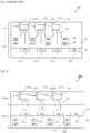
- FIG. 1 is a view illustrating the configuration of a conventional biochip having an image sensor with a front side illumination photodiode structure.
- a conventional biochip 100 having an image sensor with a front side illumination photodiode structure includes a biochip layer 100a and an image sensor layer 100b.
- the biochip layer 100a has a plurality of first reaction region 110a, second reaction region 110b and third reaction region 110c which have shapes of grooves.
- the first, second and third reaction regions 110a, 110b and 110c respectively have target samples 111a, 111b and 111c in the upper portions thereof and reference samples 112a, 112b and 112c in the lower portions thereof.
- the image sensor layer 110b has a plurality of first front side illumination photodiode 151a (PD1), second front side illumination photodiode 151b (PD2) and third front side illumination photodiode 151c (PD3) which are formed in an epitaxial layer 150 of a wafer.
- PD1 first front side illumination photodiode 151a
- PD2 second front side illumination photodiode 151b
- PD3 front side illumination photodiode 151c PD3
- a plurality of stacked metal wiring lines 131 and 133 are formed in an interlayer dielectric 130 which is formed on the upper surface of the epitaxial layer 150.
- light 120 which is emitted depending upon degrees of biochemical reactions between the target samples 111a, 111b and 111c and the reference samples 112a, 112b and 112c of the plurality of first, second and third reaction regions 110a, 110b and 110c, is likely to be absorbed by the metal wiring lines 131 and 132 which are formed over the plurality of first, second and third front side illumination photodiodes 151a, 151b and 151c, as a result of which the light sensitivity of the plurality of first, second and third front side illumination photodiodes 151a, 151b and 151c may be degraded.
- a surface treatment technology is regarded important for the attachment of bio-materials. That is to say, in order to allow the bio-materials to be easily attached to a substrate, surface treatment is performed in such a way as to provide hydrophilicity or hydrophobicity. Such surface treatment is performed mainly using plasma.
- the dark current of the photodiodes may be increased.
- solutions which are employed in the manufacture and reaction procedures of the biochip layer, may infiltrate into underlying circuits by passing through the interlayer dielectric.
- problems may be caused in that it is difficult to form the interlayer dielectric and limitations may exist in performing the surface treatment for the biochip layer and using reacting solutions, etc.
- WO 2008/140158 provides a biochip including a high-sensitivity image sensor.
- the biochip includes: a biochip layer including a plurality of reaction zones in which biochemical reactions occur formed as concaves, the reaction zone including a reference material at a lower portion and a target material at an upper portion; and an image sensor layer which is formed below the biochip layer and includes a plurality of photo detectors.
- WO 2007/148891 provides an image sensor using a back-illuminated photodiode and a manufacturing method thereof. Since a surface of the back-illuminated photodiode can be stably treated, the back-illuminated photodiode can be formed to have a low dark current, a constant sensitivity of blue light for all photodiodes, and high sensitivity.
- WO 2009/066896 discloses a fluorescent biochip diagnosis device including: an image sensor having a plurality of photo-detectors; and a band-pass filter unit having a plurality of band-pass filters formed on a plurality of the photo-detectors, wherein a plurality of the band-pass filters are implemented by forming a nanostructure pattern in a metal layer. Since the fluorescent biochip diagnosis device has little optical loss due to a short interval between the biochip and the photodetector, excellent sensitivity can be provided.
- WO 2009/011535 provides a diagnosis device in which a bio-chemical reaction between a reference sample and a target sample occurs and a result of the bio-chemical reaction can be detected and a method of manufacturing the diagnosis device.
- the diagnosis device includes an image sensor where a plurality of photo-detectors are formed; a polymer layer which is made of a polymer material and formed on an upper portion of the image sensor; and a plurality of wells which are formed corresponding to the plurality of photo-detectors on the polymer layer, wherein an inner portion of each well is empty.
- EP2221606 discloses an integrated bio-chip including; a sample detection portion including at least one light receiving device which detects fluorescent light emitted from at least one sample, a light transfer portion disposed on a light incident surface of the sample detection portion, and including at least one excitation light absorbing waveguide which absorbs an excitation light and transmits the fluorescent light emitted from the at least one sample, and a sample reaction portion disposed adjacent to an incident end of the at least one excitation light absorbing waveguide, and including at least one reaction region on which the at least one sample is attached, wherein the sample detection portion, the light transfer portion, and the sample reaction portion are integrally coupled to each other as a single component.
- biochip according to claim 1.
- the surface of the image sensor layer which is opposite to the interface with the biochip layer is in contact with a dielectric layer.
- a biochip 200 having an image sensor with a back side illumination photodiode structure includes a biochip layer 200a and an image sensor layer 200b.
- the biochip layer 200a has a plurality of reaction regions here of groove shape, including first reaction region 210a, second reaction region 210b and third reaction region 210c of groove shape.
- the first reaction region 210a has a target sample 211a in the upper portion thereof and a reference sample 212a in the lower portion thereof.
- the second reaction region 210b has a target sample 211b in the upper portion thereof and a reference sample 212b in the lower portion thereof
- the third reaction region 210c has a target sample 211c in the upper portion thereof and a reference sample 212c in the lower portion thereof.
- the target sample 211a includes a fluorescent material.
- the target sample 211a may be used to include a luminescent material which emits light by itself when external illumination is blocked.
- a representative example of the luminescent material is luciferin.
- Luciferins are bioluminescent materials. Some luciferins becomes active luciferin when activated by ATP (adenosine tri-phosphate). As the active luciferin is oxdidated under the action of luciferase and becomes oxyluciferin, chemical energy is converted into light energy and light is produced.
- the target sample 211a is used to include a fluorescent material which can generate light of a specified wavelength band by external illumination (not shown).
- the fluorescent material may be produced in the first reaction region 210a as a result of a reaction between the reference sample 212a and the target sample 211a, or may be produced in such a manner that an optional fluorescent material such as GFP (green fluorescence protein) is left in the first reaction region 210a after a specified biochemical reaction is induced between the reference sample 212a and the target sample 211a by binding the optional fluorescent material with the target sample 211a.
- GFP green fluorescence protein
- the reference sample 212a may include different materials depending upon which biochemical reaction is targeted. For example, if the biochemical reaction is an antigen-antibody reaction, the reference sample 212a may be an antigen, and if the biochemical reaction is a complementary binding of DNA bases, the reference sample 212a may be a gene which is genetically engineered to be capable of complementary binding.
- the target sample 211a is selected depending upon the reference sample 212a which is determined according to the kind of the biochemical reaction.
- the reference sample 212a is an antigen
- the target sample 211a may be blood, and the like
- the reference sample 212a is a genetically engineered gene
- the target sample 211a may be a user's gene, and the like.
- the image sensor layer 200b has a configuration which is placed on the bottom surface of the biochip layer 200a and forms a back side illumination (BSI) image sensor.
- BSI back side illumination
- the back side illumination (BSI) image sensor can be formed by performing the same processes as the conventional front side illumination (FSI) image sensor and by finally overturning a processed wafer such that the resultantly obtained image sensor can directly collect light.
- the back side illumination (BSI) image sensor collects light from the bottom portions of the photodiodes, that is, the bottom surface of the wafer.
- the image sensor layer 200b has a plurality of first back side illumination photodiode 251a (PD1), second back side illumination photodiode 251b (PD2), and third back side illumination photodiode 251c (PD3) which are formed in an epitaxial layer 250 of the wafer.
- PD1a first back side illumination photodiode 251a
- PD2 second back side illumination photodiode 251b
- PD3 third back side illumination photodiode 251c
- the first back side illumination photodiode 251a senses light 220 which is emitted from the first reaction region 210a depending upon a degree of a biochemical reaction between the target sample 211a and the reference sample 212a in the first reaction region 210a.
- the second back side illumination photodiode 251b senses light 220 which is emitted from the second reaction region 210b depending upon a degree of a biochemical reaction between the target sample 211b and the reference sample 212b in the second reaction region 210b
- the third back side illumination photodiode 251c senses light 220 which is emitted from the third reaction region 210c depending upon a degree of a biochemical reaction between the target sample 211c and the reference sample 212c in the third reaction region 210c.
- the light 220 which is respectively emitted from the first reaction region 210a, the second reaction region 210b and the third reaction region 210c, directly reaches and is absorbed by the first back side illumination photodiode 251a (PD1), the second back side illumination photodiode 251b (PD2) and the third back side illumination photodiode 251c (PD3), without passing by metal wiring lines which are stacked over the photodiodes in the formation of the conventional front side illumination (FSI) image sensor, whereby light sensitivity can be significantly improved.
- PD1a back side illumination photodiode 251a
- PD2 the second back side illumination photodiode 251b
- PD3 third back side illumination photodiode 251c
- the light sensed by the first back side illumination photodiode 251a (PD1), the second back side illumination photodiode 251b (PD2) and the third back side illumination photodiode 251c (PD3) is transduced by the photodiodes to electrical signals.
- the electrical signals are processed by a signal processing unit such as an ISP (image signal processor) 255 which is provided in the image sensor layer 200b.
- ISP image signal processor
- the upper portion of the epitaxial layer 250 includes optical filters (not shown) which transmit light of a preselected band and micro lenses (not shown) which focus light on the optical filters.
- a dielectric layer 230 is disposed under the epitaxial layer 250 and a plurality of stacked metal wiring lines 231 and 233 are formed in the dielectric layer 230.
- This structure is distinguished from the structure of the conventional front side illumination (FSI) image sensor in which an interlayer dielectric 130 is disposed on the epitaxial layer 150 and the metal wiring lines 131 and 133 are formed in the interlayer dielectric 130.
- FSI front side illumination
- the biochip layer is formed on a side which faces away from a region where circuits are formed, the characteristics of the photodiodes are not influenced by the surface treatment implemented during a procedure of manufacturing the biochip layer, and it is possible to prevent mis-operation of circuits from being caused due to infiltration of solutions used in reaction procedures.
- BSI back side illumination
Landscapes
- Health & Medical Sciences (AREA)
- Nuclear Medicine, Radiotherapy & Molecular Imaging (AREA)
- Physics & Mathematics (AREA)
- Life Sciences & Earth Sciences (AREA)
- Chemical & Material Sciences (AREA)
- Analytical Chemistry (AREA)
- Biochemistry (AREA)
- General Health & Medical Sciences (AREA)
- General Physics & Mathematics (AREA)
- Immunology (AREA)
- Pathology (AREA)
- Investigating, Analyzing Materials By Fluorescence Or Luminescence (AREA)
- Apparatus Associated With Microorganisms And Enzymes (AREA)
- Solid State Image Pick-Up Elements (AREA)
Claims (4)
- Biochip, Folgendes umfassend:eine Biochipschicht (200a); undeine Bildsensorschicht (200b) mit einer dielektrischen Schicht (230) und einer epitaxialen Schicht (250), wobei die Bildsensorschicht unmittelbar auf einer Oberfläche der Biochipschicht angeordnet ist und konfiguriert ist, Licht mit Informationen einer biochemischen Reaktion abzutasten, das aus der Biochipschicht emittiert wird,wobei die epitaxiale Schicht (250) mehrere lichtempfindliche Teile (PD1, PD2, PD3) umfasst, die konfiguriert sind, das Licht (220) zu empfangen, das aus der Biochipschicht (200a) in Richtung auf die Bildsensorschicht (200b) gerichtet ist,wobei die dielektrische Schicht (230) unmittelbar auf der epitaxialen Schicht angeordnet ist und mehrere Metallverdrahtungsleitungen umfasst,wobei die Biochipschicht (200a) mehrere Reaktionsbereiche (210a, 210b, 210c) umfasst, die rillenförmig sind, undwobei jeder der Reaktionsbereiche eine Zielprobe (211a-c) in einem ersten Abschnitt davon, wobei die Zielprobe ein Leuchtstoffmaterial umfasst, und eine Referenzprobe (212a-c) in einem zweiten Abschnitt davon aufweist, wobei die zweiten Abschnitte näher an der Bildsensorschicht (200b) sind als die ersten Abschnitte,dadurch gekennzeichnet, dassdie epitaxiale Schicht (250) zwischen der dielektrischen Schicht und der Biochipschicht (230) unmittelbar auf der Biochipschicht angeordnet ist,die mehreren lichtempfindlichen Teile Fotodiodenstrukturen für Rückseitenbeleuchtung umfassen, die unmittelbar benachbart zu der dielektrischen Schicht angeordnet sind, unddie Reaktionsbereiche und die lichtempfindlichen Teile derartig angeordnet sind, dass Licht, das aus den Reaktionsbereichen emittiert wird, die jeweiligen lichtempfindlichen Teile unmittelbar erreicht und durch diese absorbiert wird, ohne die mehreren Metallverdrahtungsleitungen und einen Filter zu passieren.
- Biochip nach Anspruch 1, wobei die Referenzprobe (211a-c) ein Antigen-Material verwendet, wenn eine biochemische Reaktion eine Antigen-Antikörper-Reaktion ist, und ein Gen verwendet, das genetisch konstruiert ist, zu einer komplementären Bindung fähig zu sein, wenn eine biochemische Reaktion eine komplementäre Bindung von DNS-Basen ist.
- Biochip nach Anspruch 1, wobei Licht, das durch die Fotodiodenstrukturen für Rückseitenbeleuchtung abgetastet wird, als elektrische Signale ausgegeben wird und die elektrischen Signale durch eine Signalverarbeitungseinheit verarbeitet werden.
- Biochip nach Anspruch 3, wobei die Bildsensorschicht einen Bildsignalprozessor (ISP) zum Verarbeiten von Signalen aus den Fotodiodenstrukturen für Rückseitenbeleuchtung umfasst.
Applications Claiming Priority (1)
| Application Number | Priority Date | Filing Date | Title |
|---|---|---|---|
| KR1020100003420A KR101062330B1 (ko) | 2010-01-14 | 2010-01-14 | 배면광 포토다이오드 구조를 갖는 이미지 센서를 구비한 바이오칩 |
Publications (3)
| Publication Number | Publication Date |
|---|---|
| EP2362418A2 EP2362418A2 (de) | 2011-08-31 |
| EP2362418A3 EP2362418A3 (de) | 2012-07-25 |
| EP2362418B1 true EP2362418B1 (de) | 2018-05-02 |
Family
ID=44201777
Family Applications (1)
| Application Number | Title | Priority Date | Filing Date |
|---|---|---|---|
| EP11150843.8A Active EP2362418B1 (de) | 2010-01-14 | 2011-01-13 | Biochip |
Country Status (4)
| Country | Link |
|---|---|
| US (1) | US8361392B2 (de) |
| EP (1) | EP2362418B1 (de) |
| KR (1) | KR101062330B1 (de) |
| CN (1) | CN102183511A (de) |
Families Citing this family (18)
| Publication number | Priority date | Publication date | Assignee | Title |
|---|---|---|---|---|
| WO2013141414A1 (en) * | 2012-03-19 | 2013-09-26 | Lg Electronics Inc. | Method for compensating output signal of optical biosensor and optical biosensor using the same |
| CN102608032A (zh) * | 2012-04-10 | 2012-07-25 | 无锡国盛精密模具有限公司 | 一种集成微透镜阵列装置 |
| US9082685B2 (en) * | 2013-06-25 | 2015-07-14 | Panasonic Intellectual Property Management Co., Ltd. | Optical-coupling semiconductor device |
| KR101506331B1 (ko) * | 2013-08-14 | 2015-04-08 | (주)실리콘화일 | 칩 구동 성능이 개선된 배면광 이미지 센서 칩 |
| KR101569515B1 (ko) * | 2014-08-13 | 2015-11-27 | (주)옵토레인 | 측광형 발광소자가 내장된 바이오칩 및 그 제조방법 |
| EP3001182B1 (de) * | 2014-09-25 | 2017-11-29 | Optolane Technologies Inc. | Verfahren zur herstellung eines biochips mit verbesserten eigenschaften bezüglich der fluoreszenzsignalerfassung, und damit hergestellter biochip |
| KR101727301B1 (ko) * | 2014-09-25 | 2017-04-14 | (주)옵토레인 | 형광 신호 감지 특성이 개선된 바이오칩의 제조방법 및 그 방법에 의해 제조된 바이오칩 |
| US12060606B2 (en) * | 2016-11-03 | 2024-08-13 | Mgi Tech Co., Ltd. | Biosensors for biological or chemical analysis and methods of manufacturing the same |
| AU2018237066B2 (en) * | 2017-03-20 | 2022-09-15 | Mgi Tech Co., Ltd. | Biosensors for biological or chemical analysis and methods of manufacturing the same |
| CN111295733B (zh) | 2017-09-19 | 2024-01-05 | 深圳华大智造科技股份有限公司 | 晶片级测序流通池制造 |
| TWI646678B (zh) * | 2017-12-07 | 2019-01-01 | 晶相光電股份有限公司 | 影像感測裝置 |
| EP3887802B1 (de) * | 2018-12-01 | 2024-05-01 | MGI Tech Co., Ltd. | Biosensor mit verbesserter lichtsammeleffizienz |
| US12196672B2 (en) | 2020-05-07 | 2025-01-14 | Hand Held Products, Inc. | Apparatuses, systems, and methods for sample testing |
| US12498328B2 (en) | 2020-05-07 | 2025-12-16 | Hand Held Products, Inc. | Apparatuses, systems, and methods for sample testing |
| US12553885B2 (en) | 2020-05-07 | 2026-02-17 | Hand Held Products, Inc. | Apparatuses, systems, and methods for sample testing |
| US11846574B2 (en) | 2020-10-29 | 2023-12-19 | Hand Held Products, Inc. | Apparatuses, systems, and methods for sample capture and extraction |
| TW202232084A (zh) | 2020-12-10 | 2022-08-16 | 美商伊路米納有限公司 | 影像感測器結構及相關方法 |
| WO2025137860A1 (zh) * | 2023-12-26 | 2025-07-03 | 深圳华大智造科技股份有限公司 | 耗材式生化物质分析设备及生化物质分析方法、一次性碱基识别装置及测序方法 |
Family Cites Families (8)
| Publication number | Priority date | Publication date | Assignee | Title |
|---|---|---|---|---|
| DE10145701A1 (de) * | 2001-09-17 | 2003-04-10 | Infineon Technologies Ag | Fluoreszenz-Biosensorchip und Fluoreszenz-Biosensorchip-Anordnung |
| JP4211696B2 (ja) | 2004-06-30 | 2009-01-21 | ソニー株式会社 | 固体撮像装置の製造方法 |
| KR100801447B1 (ko) | 2006-06-19 | 2008-02-11 | (주)실리콘화일 | 배면 광 포토다이오드를 이용한 이미지센서 및 그 제조방법 |
| KR100801448B1 (ko) | 2007-05-16 | 2008-02-11 | (주)실리콘화일 | 바이오칩 |
| KR100822672B1 (ko) | 2007-06-27 | 2008-04-17 | (주)실리콘화일 | 이미지센서를 이용한 진단장치 및 그 제조방법 |
| KR100808114B1 (ko) * | 2007-07-18 | 2008-02-29 | (주)실리콘화일 | 진단장치 및 그 제조방법 |
| KR100825087B1 (ko) * | 2007-11-23 | 2008-04-25 | (주)실리콘화일 | 형광형 바이오칩의 진단장치 |
| EP2221606A3 (de) | 2009-02-11 | 2012-06-06 | Samsung Electronics Co., Ltd. | Integrierter Biochip und Verfahren zur Herstellung des integrierten Biochips |
-
2010
- 2010-01-14 KR KR1020100003420A patent/KR101062330B1/ko active Active
- 2010-12-31 CN CN2010106238570A patent/CN102183511A/zh active Pending
-
2011
- 2011-01-05 US US12/985,083 patent/US8361392B2/en active Active
- 2011-01-13 EP EP11150843.8A patent/EP2362418B1/de active Active
Non-Patent Citations (1)
| Title |
|---|
| None * |
Also Published As
| Publication number | Publication date |
|---|---|
| CN102183511A (zh) | 2011-09-14 |
| KR20110083271A (ko) | 2011-07-20 |
| EP2362418A3 (de) | 2012-07-25 |
| KR101062330B1 (ko) | 2011-09-05 |
| EP2362418A2 (de) | 2011-08-31 |
| US8361392B2 (en) | 2013-01-29 |
| US20110172129A1 (en) | 2011-07-14 |
Similar Documents
| Publication | Publication Date | Title |
|---|---|---|
| EP2362418B1 (de) | Biochip | |
| US20250290854A1 (en) | Arrays of integrated analytical devices | |
| US10261019B2 (en) | Biosensor | |
| US8026559B2 (en) | Biosensor devices and method for fabricating the same | |
| JP5066607B2 (ja) | イメージセンサを利用した診断装置及びその製造方法 | |
| US11366062B2 (en) | Biosensor | |
| TWI521205B (zh) | Chemical detectors, biological molecular detection devices and biological molecular detection methods | |
| KR100801448B1 (ko) | 바이오칩 | |
| JP2022539633A (ja) | 光検出デバイス上の光結合構造による導波路統合 | |
| JP2021060383A (ja) | センサ装置およびその製造方法 | |
| KR101569515B1 (ko) | 측광형 발광소자가 내장된 바이오칩 및 그 제조방법 | |
| KR20160036480A (ko) | 형광 신호 감지 특성이 개선된 바이오칩의 제조방법 및 그 방법에 의해 제조된 바이오칩 | |
| CN116783472A (zh) | 每像素具有多个反应位点的传感器 |
Legal Events
| Date | Code | Title | Description |
|---|---|---|---|
| PUAI | Public reference made under article 153(3) epc to a published international application that has entered the european phase |
Free format text: ORIGINAL CODE: 0009012 |
|
| 17P | Request for examination filed |
Effective date: 20110113 |
|
| AK | Designated contracting states |
Kind code of ref document: A2 Designated state(s): AL AT BE BG CH CY CZ DE DK EE ES FI FR GB GR HR HU IE IS IT LI LT LU LV MC MK MT NL NO PL PT RO RS SE SI SK SM TR |
|
| AX | Request for extension of the european patent |
Extension state: BA ME |
|
| PUAL | Search report despatched |
Free format text: ORIGINAL CODE: 0009013 |
|
| AK | Designated contracting states |
Kind code of ref document: A3 Designated state(s): AL AT BE BG CH CY CZ DE DK EE ES FI FR GB GR HR HU IE IS IT LI LT LU LV MC MK MT NL NO PL PT RO RS SE SI SK SM TR |
|
| AX | Request for extension of the european patent |
Extension state: BA ME |
|
| RIC1 | Information provided on ipc code assigned before grant |
Ipc: G01N 21/00 20060101ALI20120619BHEP Ipc: G01N 21/64 20060101ALI20120619BHEP Ipc: H01L 27/146 20060101AFI20120619BHEP |
|
| RAP1 | Party data changed (applicant data changed or rights of an application transferred) |
Owner name: LEE, DO YOUNG |
|
| RAP1 | Party data changed (applicant data changed or rights of an application transferred) |
Owner name: OPTOLANE TECHNOLOGIES INC. |
|
| 17Q | First examination report despatched |
Effective date: 20160310 |
|
| GRAP | Despatch of communication of intention to grant a patent |
Free format text: ORIGINAL CODE: EPIDOSNIGR1 |
|
| STAA | Information on the status of an ep patent application or granted ep patent |
Free format text: STATUS: GRANT OF PATENT IS INTENDED |
|
| INTG | Intention to grant announced |
Effective date: 20171130 |
|
| RAP1 | Party data changed (applicant data changed or rights of an application transferred) |
Owner name: OPTOLANE TECHNOLOGIES INC. |
|
| GRAS | Grant fee paid |
Free format text: ORIGINAL CODE: EPIDOSNIGR3 |
|
| GRAA | (expected) grant |
Free format text: ORIGINAL CODE: 0009210 |
|
| STAA | Information on the status of an ep patent application or granted ep patent |
Free format text: STATUS: THE PATENT HAS BEEN GRANTED |
|
| AK | Designated contracting states |
Kind code of ref document: B1 Designated state(s): AL AT BE BG CH CY CZ DE DK EE ES FI FR GB GR HR HU IE IS IT LI LT LU LV MC MK MT NL NO PL PT RO RS SE SI SK SM TR |
|
| REG | Reference to a national code |
Ref country code: GB Ref legal event code: FG4D |
|
| REG | Reference to a national code |
Ref country code: CH Ref legal event code: EP Ref country code: AT Ref legal event code: REF Ref document number: 996138 Country of ref document: AT Kind code of ref document: T Effective date: 20180515 |
|
| REG | Reference to a national code |
Ref country code: DE Ref legal event code: R096 Ref document number: 602011047962 Country of ref document: DE |
|
| REG | Reference to a national code |
Ref country code: IE Ref legal event code: FG4D |
|
| REG | Reference to a national code |
Ref country code: NL Ref legal event code: MP Effective date: 20180502 |
|
| REG | Reference to a national code |
Ref country code: LT Ref legal event code: MG4D |
|
| PG25 | Lapsed in a contracting state [announced via postgrant information from national office to epo] |
Ref country code: SE Free format text: LAPSE BECAUSE OF FAILURE TO SUBMIT A TRANSLATION OF THE DESCRIPTION OR TO PAY THE FEE WITHIN THE PRESCRIBED TIME-LIMIT Effective date: 20180502 Ref country code: BG Free format text: LAPSE BECAUSE OF FAILURE TO SUBMIT A TRANSLATION OF THE DESCRIPTION OR TO PAY THE FEE WITHIN THE PRESCRIBED TIME-LIMIT Effective date: 20180802 Ref country code: FI Free format text: LAPSE BECAUSE OF FAILURE TO SUBMIT A TRANSLATION OF THE DESCRIPTION OR TO PAY THE FEE WITHIN THE PRESCRIBED TIME-LIMIT Effective date: 20180502 Ref country code: NO Free format text: LAPSE BECAUSE OF FAILURE TO SUBMIT A TRANSLATION OF THE DESCRIPTION OR TO PAY THE FEE WITHIN THE PRESCRIBED TIME-LIMIT Effective date: 20180802 Ref country code: LT Free format text: LAPSE BECAUSE OF FAILURE TO SUBMIT A TRANSLATION OF THE DESCRIPTION OR TO PAY THE FEE WITHIN THE PRESCRIBED TIME-LIMIT Effective date: 20180502 Ref country code: ES Free format text: LAPSE BECAUSE OF FAILURE TO SUBMIT A TRANSLATION OF THE DESCRIPTION OR TO PAY THE FEE WITHIN THE PRESCRIBED TIME-LIMIT Effective date: 20180502 |
|
| PG25 | Lapsed in a contracting state [announced via postgrant information from national office to epo] |
Ref country code: GR Free format text: LAPSE BECAUSE OF FAILURE TO SUBMIT A TRANSLATION OF THE DESCRIPTION OR TO PAY THE FEE WITHIN THE PRESCRIBED TIME-LIMIT Effective date: 20180803 Ref country code: NL Free format text: LAPSE BECAUSE OF FAILURE TO SUBMIT A TRANSLATION OF THE DESCRIPTION OR TO PAY THE FEE WITHIN THE PRESCRIBED TIME-LIMIT Effective date: 20180502 Ref country code: HR Free format text: LAPSE BECAUSE OF FAILURE TO SUBMIT A TRANSLATION OF THE DESCRIPTION OR TO PAY THE FEE WITHIN THE PRESCRIBED TIME-LIMIT Effective date: 20180502 Ref country code: LV Free format text: LAPSE BECAUSE OF FAILURE TO SUBMIT A TRANSLATION OF THE DESCRIPTION OR TO PAY THE FEE WITHIN THE PRESCRIBED TIME-LIMIT Effective date: 20180502 Ref country code: RS Free format text: LAPSE BECAUSE OF FAILURE TO SUBMIT A TRANSLATION OF THE DESCRIPTION OR TO PAY THE FEE WITHIN THE PRESCRIBED TIME-LIMIT Effective date: 20180502 |
|
| REG | Reference to a national code |
Ref country code: AT Ref legal event code: MK05 Ref document number: 996138 Country of ref document: AT Kind code of ref document: T Effective date: 20180502 |
|
| PG25 | Lapsed in a contracting state [announced via postgrant information from national office to epo] |
Ref country code: PT Free format text: LAPSE BECAUSE OF FAILURE TO SUBMIT A TRANSLATION OF THE DESCRIPTION OR TO PAY THE FEE WITHIN THE PRESCRIBED TIME-LIMIT Effective date: 20180903 |
|
| PG25 | Lapsed in a contracting state [announced via postgrant information from national office to epo] |
Ref country code: CZ Free format text: LAPSE BECAUSE OF FAILURE TO SUBMIT A TRANSLATION OF THE DESCRIPTION OR TO PAY THE FEE WITHIN THE PRESCRIBED TIME-LIMIT Effective date: 20180502 Ref country code: RO Free format text: LAPSE BECAUSE OF FAILURE TO SUBMIT A TRANSLATION OF THE DESCRIPTION OR TO PAY THE FEE WITHIN THE PRESCRIBED TIME-LIMIT Effective date: 20180502 Ref country code: DK Free format text: LAPSE BECAUSE OF FAILURE TO SUBMIT A TRANSLATION OF THE DESCRIPTION OR TO PAY THE FEE WITHIN THE PRESCRIBED TIME-LIMIT Effective date: 20180502 Ref country code: AT Free format text: LAPSE BECAUSE OF FAILURE TO SUBMIT A TRANSLATION OF THE DESCRIPTION OR TO PAY THE FEE WITHIN THE PRESCRIBED TIME-LIMIT Effective date: 20180502 Ref country code: EE Free format text: LAPSE BECAUSE OF FAILURE TO SUBMIT A TRANSLATION OF THE DESCRIPTION OR TO PAY THE FEE WITHIN THE PRESCRIBED TIME-LIMIT Effective date: 20180502 Ref country code: PL Free format text: LAPSE BECAUSE OF FAILURE TO SUBMIT A TRANSLATION OF THE DESCRIPTION OR TO PAY THE FEE WITHIN THE PRESCRIBED TIME-LIMIT Effective date: 20180502 Ref country code: SK Free format text: LAPSE BECAUSE OF FAILURE TO SUBMIT A TRANSLATION OF THE DESCRIPTION OR TO PAY THE FEE WITHIN THE PRESCRIBED TIME-LIMIT Effective date: 20180502 |
|
| REG | Reference to a national code |
Ref country code: DE Ref legal event code: R097 Ref document number: 602011047962 Country of ref document: DE |
|
| PG25 | Lapsed in a contracting state [announced via postgrant information from national office to epo] |
Ref country code: SM Free format text: LAPSE BECAUSE OF FAILURE TO SUBMIT A TRANSLATION OF THE DESCRIPTION OR TO PAY THE FEE WITHIN THE PRESCRIBED TIME-LIMIT Effective date: 20180502 |
|
| PLBE | No opposition filed within time limit |
Free format text: ORIGINAL CODE: 0009261 |
|
| STAA | Information on the status of an ep patent application or granted ep patent |
Free format text: STATUS: NO OPPOSITION FILED WITHIN TIME LIMIT |
|
| 26N | No opposition filed |
Effective date: 20190205 |
|
| PG25 | Lapsed in a contracting state [announced via postgrant information from national office to epo] |
Ref country code: SI Free format text: LAPSE BECAUSE OF FAILURE TO SUBMIT A TRANSLATION OF THE DESCRIPTION OR TO PAY THE FEE WITHIN THE PRESCRIBED TIME-LIMIT Effective date: 20180502 |
|
| PG25 | Lapsed in a contracting state [announced via postgrant information from national office to epo] |
Ref country code: MC Free format text: LAPSE BECAUSE OF FAILURE TO SUBMIT A TRANSLATION OF THE DESCRIPTION OR TO PAY THE FEE WITHIN THE PRESCRIBED TIME-LIMIT Effective date: 20180502 |
|
| REG | Reference to a national code |
Ref country code: CH Ref legal event code: PL |
|
| PG25 | Lapsed in a contracting state [announced via postgrant information from national office to epo] |
Ref country code: LU Free format text: LAPSE BECAUSE OF NON-PAYMENT OF DUE FEES Effective date: 20190113 |
|
| REG | Reference to a national code |
Ref country code: BE Ref legal event code: MM Effective date: 20190131 |
|
| REG | Reference to a national code |
Ref country code: IE Ref legal event code: MM4A |
|
| PG25 | Lapsed in a contracting state [announced via postgrant information from national office to epo] |
Ref country code: AL Free format text: LAPSE BECAUSE OF FAILURE TO SUBMIT A TRANSLATION OF THE DESCRIPTION OR TO PAY THE FEE WITHIN THE PRESCRIBED TIME-LIMIT Effective date: 20180502 Ref country code: BE Free format text: LAPSE BECAUSE OF NON-PAYMENT OF DUE FEES Effective date: 20190131 |
|
| PG25 | Lapsed in a contracting state [announced via postgrant information from national office to epo] |
Ref country code: CH Free format text: LAPSE BECAUSE OF NON-PAYMENT OF DUE FEES Effective date: 20190131 Ref country code: LI Free format text: LAPSE BECAUSE OF NON-PAYMENT OF DUE FEES Effective date: 20190131 |
|
| PG25 | Lapsed in a contracting state [announced via postgrant information from national office to epo] |
Ref country code: IE Free format text: LAPSE BECAUSE OF NON-PAYMENT OF DUE FEES Effective date: 20190113 |
|
| PG25 | Lapsed in a contracting state [announced via postgrant information from national office to epo] |
Ref country code: TR Free format text: LAPSE BECAUSE OF FAILURE TO SUBMIT A TRANSLATION OF THE DESCRIPTION OR TO PAY THE FEE WITHIN THE PRESCRIBED TIME-LIMIT Effective date: 20180502 |
|
| PG25 | Lapsed in a contracting state [announced via postgrant information from national office to epo] |
Ref country code: MT Free format text: LAPSE BECAUSE OF NON-PAYMENT OF DUE FEES Effective date: 20190113 |
|
| PG25 | Lapsed in a contracting state [announced via postgrant information from national office to epo] |
Ref country code: CY Free format text: LAPSE BECAUSE OF FAILURE TO SUBMIT A TRANSLATION OF THE DESCRIPTION OR TO PAY THE FEE WITHIN THE PRESCRIBED TIME-LIMIT Effective date: 20180502 |
|
| PG25 | Lapsed in a contracting state [announced via postgrant information from national office to epo] |
Ref country code: IS Free format text: LAPSE BECAUSE OF FAILURE TO SUBMIT A TRANSLATION OF THE DESCRIPTION OR TO PAY THE FEE WITHIN THE PRESCRIBED TIME-LIMIT Effective date: 20180902 |
|
| PG25 | Lapsed in a contracting state [announced via postgrant information from national office to epo] |
Ref country code: HU Free format text: LAPSE BECAUSE OF FAILURE TO SUBMIT A TRANSLATION OF THE DESCRIPTION OR TO PAY THE FEE WITHIN THE PRESCRIBED TIME-LIMIT; INVALID AB INITIO Effective date: 20110113 |
|
| PG25 | Lapsed in a contracting state [announced via postgrant information from national office to epo] |
Ref country code: MK Free format text: LAPSE BECAUSE OF FAILURE TO SUBMIT A TRANSLATION OF THE DESCRIPTION OR TO PAY THE FEE WITHIN THE PRESCRIBED TIME-LIMIT Effective date: 20180502 |
|
| REG | Reference to a national code |
Ref country code: DE Ref legal event code: R079 Ref document number: 602011047962 Country of ref document: DE Free format text: PREVIOUS MAIN CLASS: H01L0027146000 Ipc: H10F0039180000 |
|
| PGFP | Annual fee paid to national office [announced via postgrant information from national office to epo] |
Ref country code: GB Payment date: 20251222 Year of fee payment: 16 |
|
| PGFP | Annual fee paid to national office [announced via postgrant information from national office to epo] |
Ref country code: FR Payment date: 20251223 Year of fee payment: 16 |
|
| PGFP | Annual fee paid to national office [announced via postgrant information from national office to epo] |
Ref country code: DE Payment date: 20251222 Year of fee payment: 16 |
|
| PGFP | Annual fee paid to national office [announced via postgrant information from national office to epo] |
Ref country code: IT Payment date: 20251223 Year of fee payment: 16 |