EP2362632B1 - Appareil et procédé de traitement d'images - Google Patents
Appareil et procédé de traitement d'images Download PDFInfo
- Publication number
- EP2362632B1 EP2362632B1 EP11150691.1A EP11150691A EP2362632B1 EP 2362632 B1 EP2362632 B1 EP 2362632B1 EP 11150691 A EP11150691 A EP 11150691A EP 2362632 B1 EP2362632 B1 EP 2362632B1
- Authority
- EP
- European Patent Office
- Prior art keywords
- band
- processing
- image processing
- area
- band area
- Prior art date
- Legal status (The legal status is an assumption and is not a legal conclusion. Google has not performed a legal analysis and makes no representation as to the accuracy of the status listed.)
- Not-in-force
Links
Images


Classifications
-
- H—ELECTRICITY
- H04—ELECTRIC COMMUNICATION TECHNIQUE
- H04N—PICTORIAL COMMUNICATION, e.g. TELEVISION
- H04N1/00—Scanning, transmission or reproduction of documents or the like, e.g. facsimile transmission; Details thereof
- H04N1/46—Colour picture communication systems
Definitions
- the present invention relates to an image processing apparatus and an image processing method for dividing image data into a plurality of band areas and performing local image processing for each band area.
- Ordinarily local (neighborhood) image processing such as spatial filtering is performed on the image data, when performing image forming based on digital image data.
- This local image processing is image processing in which some calculation is performed using all pixels included in a spatial filtering area that includes a pixel to be processed (referred to below as a pixel of interest).
- the local image processing is performed as successive processing in band units.
- spatial filtering such as edge enhancement processing or blur processing is performed on the image data.
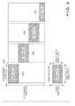
- Technology is known in which, for example as shown in FIG. 3 , when performing spatial filtering on digital image data 300, the digital image data is divided into areas, and the local image processing is performed for each individual area (for example, see U.S. Patent No. 6,587,158 ).
- the whole of one item of digital image data is divided into strips (rectangular strips) in a sub-scanning direction when reading (or when outputting) that digital image data, and various image processing is performed successively for each divided area.
- band areas the areas of these respective divided strips are referred to as band areas
- a storage area where the band areas are developed is referred to as a band memory
- band division an action of dividing an image
- band processing performed on a band area
- the band memory may be secured in any storage area of a system, but in the description given here, the band memory is secured within a main memory in order to simplify the description.
- a first band area 301 is developed in the band memory in the main memory, and image processing is performed.
- a second band area 302 is developed by overwriting the band memory where the first band area 301 was developed, and image processing is performed.
- a third band area 303 is developed by overwriting the band memory where the second band area 302 was developed, and image processing is performed.
- a fourth band area 304 is developed by overwriting the band memory where the third band area 303 was developed, and image processing is performed. As is seen from FIG.
- the size in the longer side direction (length) is the width in the main scanning direction and therefore is the same for each of the band areas 301 to 304, but the size in the shorter side direction (height) is not necessarily the same for each of the band areas 301 to 304.
- the first to third band areas 301 to 303 have the same height
- the fourth band area 304 is a portion of the entire digital image data that was not assigned to the first to third band areas, and therefore ordinarily does not have the same height as the other band areas. Consequently, the size of the storage area secured as the band memory in the main memory is determined according to the band area that has the largest size in the height direction (in the case of FIG. 3 , the first to third band areas 301 to 303).
- each band area is expressed with a size of length direction x height direction, with the length direction being the longer side direction of the band area and the height direction being the shorter side direction.
- the length of the band areas 301 to 304 is the width in the main scanning direction of the digital image data
- the band height (height of the band area) is an arbitrary value.
- Scanning of pixels in each band area can be controlled such that the scanning is performed in the height direction of the band area and not in the length direction.
- By performing scanning in the height direction it is possible to prescribe the capacity of a delay memory that holds processed pixels necessary for local image processing at the size of a height that is less than the length of the respective band areas, and thus memory saving can be realized (for example, see Japanese Patent Laid-Open No. 2006-139606 ).
- Error diffusion is processing for converting multi-tone digital image data to digital image data of fewer tones, such as binary digital image data, and is one type of digital halftoning processing.
- a pixel of interest is quantized to a quantization representative value based on a threshold, a quantization error that occurred at that time is diffused to tone values of neighbor pixels of the pixel of interest, the quantization error being a difference between the pixel of interest and the quantization representative value that occurred when performing quantization, and the respective tone values of these neighbor pixels are successively converted to digital halftoning data.
- a feature of error diffusion is propagating the quantization error to the neighbor pixels, but when using both the above-described band processing and error diffusion, the quantization error is not correctly propagated at the band border, and so discontinuous deteriorated image quality unintentionally occurs in the digital halftoning data after error diffusion.
- a phenomenon called “sweep out” occurs in which dots are not formed until a quantization error is sufficiently accumulated. This "sweep out" is likely to occur at a band border, so that a problem also occurs in which a gap where a dot is not formed is visible as a discontinuous line or the like.
- the present invention was made in order to address the problems described above, and provides an image processing apparatus having the following function and an image processing method. That is, when performing local image processing for each of band areas obtained by dividing image data, deterioration of image quality at a band border is suppressed, while realizing a smaller-scale circuit configuration.
- the present invention in its first aspect provides an image processing apparatus as specified in claims 1 to 6.
- the present invention in its second aspect provides an image processing method as specified in claim 7.
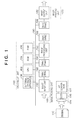
- FIG. 1 is a block diagram that shows an example of the overall configuration of an image processing apparatus in the present embodiment.
- a CPU circuit unit 100 includes a CPU 102 for calculation and control, a ROM 104 that stores fixed data and programs, a RAM 106 used for temporarily saving data and loading programs, an external storage apparatus 108, and so forth.
- the CPU circuit unit 100 controls an image input unit 130, an image processing unit 150, an image output unit 160, and so forth, and performs central control of sequences of the image processing apparatus of the present embodiment.
- the external storage apparatus 108 is a storage medium such as a disk that stores parameters, programs, correction data, and so forth used by the image processing apparatus of the present embodiment. Data, programs, and so forth of the RAM 106 may be loaded from the external storage apparatus 108.
- image data can be input is applicable as the image input unit 130; for example, a captured image may be input via a cable, or image data may be downloaded via the Internet or the like.
- an image reading unit 120 that reads an original 110 and generates image data of the original 110 is adopted as the image input unit 130.
- the image reading unit 120 has a lens 124, a CCD sensor 126, an analog signal processing unit 127, and so forth.
- image information of the original 110 is formed on the CCD sensor 126 via the lens 124, and converted to an analog electrical signal of R(Red), G(Green), and B(Blue).
- the image information is input to the analog signal processing unit 127, then correction and so forth are performed for each of the colors R, G, and B, and then analog/digital conversion (A/D conversion) of the signal is performed.
- A/D conversion analog/digital conversion
- the digital image signal generated by the image reading unit 120 is stored in the RAM 106 of the CPU circuit unit 100 via a shared bus 190 by a DMAC (Direct Memory Access Controller) 192 whose operation has been set in advance.
- the CPU 102 controls the DMAC 192.
- the CPU 102 by controlling a DMAC 194, reads out the digital image signal stored in the RAM 106 and inputs that digital image signal to the image processing unit 150.
- the image processing unit 150 with respect to the digital image signal that has been input, performs correction of individual difference of a reading element of a sensor device such as a scanner for example, color correction such as input gamma correction, and so forth, and normalizes the read image to create a digital image signal with a certain level.
- the digital image signal after processing is again stored in the RAM 106 by a DMAC 196 for which a write operation has been set in advance.
- the image processing unit 150 also, with respect to the digital image signal that has been input, performs various image processing for printing such as input color correction, spatial filtering, color space conversion, density correction, and halftoning processing, thus creating a printable digital image signal.
- the printable digital image signal that has been created is again stored in the RAM 106 by the DMAC 196.
- the CPU 102 controls a DMAC 198 to read out the image-processed digital image signal stored in the RAM 106 and output that digital image signal to an image printing unit 170.
- the image printing unit 170 is configured as a printer provided with a printing/output unit (not shown) such as a raster plotter using an inkjet head, a thermal head, or the like, for example, and the image printing unit 170 forms an image on a recording paper based on the digital image signal that has been input.
- a printing/output unit such as a raster plotter using an inkjet head, a thermal head, or the like, for example, and the image printing unit 170 forms an image on a recording paper based on the digital image signal that has been input.
- the image that has been read by the image reading unit 120 in FIG. 1 is being temporarily stored in the RAM 106, as described above.
- the RAM 106 is often configured with an inexpensive DRAM, and in order to perform data reading/writing via DMACs as described above, it is possible to adopt a configuration in which data can be accessed in units such that reading/writing without a decrease in DRAM performance is possible.
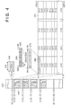
- FIG. 4 an exemplary data structure of a digital image signal and a storage method thereof in the RAM 106 will be described.
- reference numeral 400 denotes the data structure of the digital image signal stored in the RAM 106.
- an area from IMG_AREA_STR_ADDR to IMG_AREA_END_ADDR is an area where data of one processing unit in the image processing is stored.
- data of four colors from SO_IMG to S3_IMG is stored in the area within this processing unit. This data of four colors has been converted to data for a first color K (Black), a second color M (Magenta), a third color C (Cyan), and a fourth color Y (Yellow) by performing color space conversion, density correction, and so forth on an image that was read by the image reading unit 120.
- the data of these first to fourth colors is stored in the RAM 106 in a frame-sequential (planar format) manner.
- a minimum unit (access unit) of data capacity stored for each color is 32 bytes of 32 bits x 8 words, as indicated by reference numeral 408. Accordingly, the storage capacity of data from SO_IMG to S3_IMG is an integer multiple of 32 bytes.
- Reference numeral 450 denotes the image data (below, K data) of the first color K (Black) that has been stored in the area of SO_IMG 420.
- Reference numeral 460 denotes the above-described 32 bytes of access unit data within the K data 450, and in this example, there are MxN items of the access unit data 460 within the K data 450. Eight items of data are packed within the access unit data 460 as denoted by reference numeral 470, and in one of those items of data, four items (four pixels) of 8-bit K (Black) data are packed as denoted by reference numeral 480. Accordingly, the K data 450 indicated by a thick-lined frame in FIG. 4 has a size of 8x4xMxN pixels.
- the digital image signal having the above-described data structure is read out from the RAM 106, and is input to the image processing unit 150.
- FIG. 2 shows the configuration of an image processing circuit unit 200 that is an example of the main circuit configuration possessed by the image processing unit 150 of the present embodiment.
- a processing image input circuit 220 receives various data via a bus 205, and when the packed digital image signal shown in FIG. 4 has been received, the packed digital image signal is unpacked to a digital image signal of pixel units. The unpacked digital image signal is forwarded to subsequent image processing circuits (1) 230, (2) 240, ..., (P) 280, and various correction or image processing is performed. Then, in a processing image output circuit 290, a digital image signal is created that has been re-packed to data in the 32-byte units shown in FIG.
- image processing circuits (1) 230 to (P) 280 in any of those image processing circuits, image processing such as input color correction, spatial filtering, color space conversion, density correction, and halftoning processing are respectively performed.
- image processing circuits (1) 230 to (P) 280 for example, processing for one color (one plane) may be performed, or processing for a set of several colors such as RGB or CMYK may be performed.
- image processing is successively performed for each of a plurality of band areas obtained by dividing image data in a fixed direction.
- image processing specialized for band processing is performed using a band area coordinate system that differs from a digital image data coordinate system (main scanning direction x sub-scanning direction).
- the band area coordinate system is expressed by a length direction x a height direction that correspond to a longer side direction x a shorter side direction of the band area, as shown in the lower portion of FIG. 3 described above.
- the length direction of the band area corresponds to the size of the image data in the main scanning direction or the sub-scanning direction, but the size of the band area in the height direction can be set arbitrarily according to a division size. Although described in detail later, the size in the height direction of the band area can be set to a smaller size than the size in the length direction.
- the processing areas within the band area where error diffusion is performed differ for each color (each plane), and the processing border of each band is caused to differ for each color.
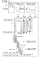
- FIG. 5 shows an example of performing a sequence of band processing in which a band area is divided in the sub-scanning direction of the image data, then a band area 500 is processed, then a band area 510 is processed, and then a band area 520 is processed.
- the middle portion of FIG. 5 shows exemplary band height settings for the band area 510 in this sequence of band processing.
- First color data 512 is data of a K plane
- second color data 514 is data of an M plane
- third color data 516 is data of a C plane
- fourth color data 518 is data of a Y plane.
- a processing range of error diffusion indicated by "starting height" to "ending height” is set so as to differ for each color data.
- the height of the band area 510 is set such that an overlapping area that overlaps an adjacent band area encompasses a border of the entire application range (the range surrounded by diagonal lines in FIG. 5 ) of the first color data 512 to the fourth color data 518.
- numbers of pixels in the overlapping area at the upper end and the lower end respectively of the band area are referred to as a number of upper end overlapping pixels and a number of lower end overlapping pixels.
- the lower portion of FIG. 5 shows a relationship between respective band areas and the processing range and the processing border for each color thereof, in a sequence of a plurality of instances of band processing.
- each band area overlaps with the preceding and subsequent band areas, and that overlapping area is understood to be determined according to the processing range of each color in that band. That is, in the upper end portion and the lower end portion respectively in the band area, the area that includes the band borders of all colors is set as the overlapping area indicated by the number of upper end overlapping pixels and the number of lower end overlapping pixels.
- the data of these overlapping areas is obtained in an overlapping manner from the RAM 106, and is input to the image processing circuit unit 200.
- the overlapping area (the number of overlapping pixels) between band areas that is set in the present embodiment can be any size, as long as it is possible to perform supplementation such that between vertically continuous band areas the processing range of each color is continuous.
- the processing range of each color in each band is made to differ, that is, the band height that is the actual subject of processing is made to differ for each color.
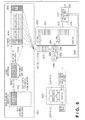
- a portion surrounded by a dotted line 605 schematically indicates the digital image data stored in the RAM 106.
- reference numeral 600 denotes the entire digital image data, and from the entire data 600, a band area 610 having a band height that has been set as described with reference to FIG. 5 is extracted, and image processing is performed.
- the band area 610 on which processing is to be performed has a configuration as indicated by reference numerals 620 to 640 to the right side of the band area 610.
- a height Bdh in the band area coordinate system is 16 lines (16 pixels), and a length Bdl is 8x4xM pixels as indicated by reference numerals 630 to 640.
- reference numerals 630 to 640 denote items of access unit data (1) to (M) described later, and the size of each of those items of data is 16 lines x (8x4) pixels.
- a CPU 680 shown below the dotted line 605 sets read-out information of the band area 610 from the RAM 106 to a DMAC 690 via a shared bus 685.
- the CPU 680 corresponds to the CPU 102 shown in FIG. 1
- the DMAC 690 likewise corresponds to the DMAC 194.
- the read-out information set to the DMAC 690 includes information regarding a start address of the band area 610 in the RAM 106, a continuous read-out amount that indicates how many times to continuously read out data in 32-byte units, an increment address, and a number of repetitions.
- the continuous read-out amount is one time (32 bytes)
- the increment address is 32 bytes x M, which is the data amount of one line
- the number of repetitions is 16 times.
- the CPU 680 via the shared bus 685 to the DMAC 690, instructs also a write start address of the shared buffer 660 that is a write destination of acquired data.
- written data is temporarily saved to an area 662 in the shared buffer 660, so the write start address for the shared buffer 660 is a start address SO_BUF_STR_ADDR of the area 662.
- the DMAC 690 receives the instruction from the CPU 680, and with respect to one color among the image data that has been saved in the RAM 106, reads out any of the items of access unit data (1) 630 to (M) 640 in the band area 620.
- the access unit data read out is denoted by reference numeral 650.
- the DMAC 690 stores the acquired data 650 in the area 662 of the shared buffer 660 via a shared bus 694, and then notifies the CPU 680 that transfer has ended with an interrupt signal 692.
- the CPU 680 sets the read-out information of the shared buffer 660 to the processing image input circuit 670 via a shared bus 688 and activates the processing image input circuit 670.
- the read-out information is information regarding each of a band area height described later, a starting height and an ending height of the processed color in this band area, an image data format, the read-out start address S0_BUF_STR_ADDR of the shared buffer, and so forth.
- the processing image input circuit 670 by reading and accessing the shared buffer 660 via a control signal 672 such as a chip selection signal or an address signal, acquires read data 674. Then, pixel data (a pixel value) of one color of one pixel unit is selected from the acquired read data 674, and the pixel data is output to an internal bus 676 (corresponding to an internal bus 225 shown in FIG. 2 ) of the image processing circuit unit 200.
- a control signal 672 such as a chip selection signal or an address signal
- pixels of interest are successively determined by scanning pixels orthogonal to the length direction of the band area.
- the length direction of the band area is the same as the main scanning direction of the image data when reading (or when outputting).
- the scanning direction in a band in the present embodiment is the sub-scanning direction when reading (the shorter side direction of the band area, referred to below as the height direction), orthogonal to the main scanning direction when reading (the longer side direction of the band area). Scanning within the band in the direction orthogonal to the main scanning direction when reading the band area in this way is referred to below as cross band processing.
- the shared buffer 660 may also be configured with two or more buffers 666 and 667.
- one buffer is shared by the DMAC 690 and the processing image input circuit 670, so it is necessary to perform operation in a time-sharing fashion, but by adopting a configuration with a plurality of buffers, processing can be accelerated. That is, while the processing image input circuit 670 is acquiring the pixel data from the shared buffer 667, the DMAC 690 can transfer data from the RAM 106 to the shared buffer 666, so the processing of the DMAC 690 and the processing image input circuit 670 can be performed in parallel.
- a configuration is acceptable in which, when performing the image processing of the band area 620 (610) of the digital image data, processing by the DMAC 690 is repeated with respect to each of the items of access unit data (1) 630 to (M) 640 in the band area 620. Moreover, the same processing may be repeated with respect to the first color to the fourth color.
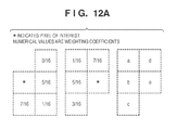
- FIG. 12A shows an example of error diffusion coefficients used for error diffusion in the present embodiment.
- an error distribution is shown in which pixels of interest indicated by * are diffused in pixels within a neighborhood area.
- the center portion of FIG. 12A shows a filter used when calculating an error diffused from a neighbor pixel for a pixel of interest *, when error diffusion has been performed using the above error diffusion coefficients. This filter has a form that is point-symmetrical to the above error diffusion coefficients.
- FIG. 12A shows an example of error diffusion coefficients used for error diffusion in the present embodiment.
- an error distribution is shown in which pixels of interest indicated by * are diffused in pixels within a neighborhood area.
- the center portion of FIG. 12A shows a filter used when calculating an error diffused from a neighbor pixel for a pixel of interest *, when error diffusion has been performed using the above error diffusion coefficients.
- This filter has a form that is point-symmetrical to the above error diffusion coefficients.
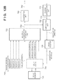
- FIG. 12B shows an exemplary configuration of an error diffusion circuit in the present embodiment.
- This error diffusion circuit as described above, is any of the image processing circuits (1) 230 to (P) 280 in the image processing circuit unit 200.
- FIG. 12B shows a state in which the pixel of interest e has been input, and in order to process this pixel of interest e, quantization errors ea to ed obtained as calculation results when processing the above pixel positions a to d are necessary.
- the quantization errors ea, eb, and ec of the pixel positions a, b, and c are already stored in a delay memory 740.
- the quantization error ed of the pixel position d that was processed immediately prior to the pixel of interest e is already stored in a delay register 746.
- the quantization errors ea, eb, and ec are extracted from the delay memory 740 via a delay circuit 744, and input to a multiply-accumulation operation unit 755.
- the quantization error ed is also input from the delay register 746 to the multiply-accumulation operation unit 755.
- four types of error diffusion coefficients stored in an error diffusion coefficient register 750 are input to the multiply-accumulation operation unit 755.
- multiply-accumulation operation unit 755 for each of the quantization errors ea to ed, weighting by the corresponding error diffusion coefficient is performed, and the sum of the value after weighting and the pixel of interest value e is output as a multiply-accumulation operation result 758.
- a quantization unit 760 quantizes the multiply-accumulation operation result 758 from the multiply-accumulation operation unit 755 to a predetermined quantization representative value based on a predetermined threshold, and outputs a quantization result 762.
- An inverse quantization unit 770 inverse-quantizes the quantization result 762 from the quantization unit 760 to return the quantization result 762 to the quantization representative value, and outputs this as an inverse-quantization result 772.
- a subtraction unit 780 the difference between the multiply-accumulation operation result 758 output from the multiply-accumulation operation unit 755 and the inverse-quantization result 772 output from the inverse quantization unit 770 is calculated, and output as a quantization error ee.
- the quantization error ee that has been output from the subtraction unit 780 is stored in the delay register 746, and is used when processing the next pixel. Also, the quantization error ed that was used in order to process the pixel of interest e is stored in the delay memory 740 via the delay circuit 744, and is used when processing a pixel of the next line in the length direction of the band area.
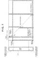
- FIG. 7 shows how quantization errors are stored in the delay memory 740 when error diffusion is performed by the error diffusion circuit shown in FIG. 12B .
- cross band processing is performed, so the pixel scanning direction when processing the band area 510 is the orthogonal direction (height direction) to the length direction of the band area, as indicated by arrow 710 in FIG. 7 .
- first scanning of an upper left pixel as the pixel of interest e is started, and scanning of a 1-pixel column in the height direction is performed to determine the pixel of interest e.
- the pixel of interest e is shifted by one pixel in the length direction of the band area, and scanning in the height direction is performed from the pixel at the upper end to the pixel at the lower end in the new pixel column in the band area 510. This sort of scanning in the height direction is repeated until processing finishes for all pixels in the band area.
- FIG. 7 shows, in the error diffusion for the first color data 512 shown in FIG. 5 , the relationship between the pixel of interest e during that scanning and the pixel position held in the delay memory 740 during processing of the pixel of interest e.
- cross band processing is performed, so in FIG. 7 the pixel of interest e shifts sequentially in the height direction from the upper left of the band area, and examples are shown of a case when the pixel of interest e is positioned at the upper end of the band area, a case when the pixel of interest e is positioned at the center of the band area, and a case when the pixel of interest e is positioned at the lower end of the band area.
- the quantization error obtained by the instance of scanning prior to scanning for the pixel of interest e and the quantization error obtained during the present scanning are held in the delay memory 740.
- the quantization error obtained by the prior instance of scanning is successively replaced by the quantization error obtained by the present instance of scanning.
- the number of pixels for which the delay memory 740 holds a quantization error depends on the band height.
- a configuration is acceptable if the delay memory 740 is capable of holding at least calculation results for a number of pixels corresponding to the band height.
- the band height that corresponds to the shorter side direction of the band area is smaller than the size in the longer side direction, that is, the band length that corresponds to the width of the recording paper on which the entire image is ordinarily formed, so the number of pixels to be held by the delay memory 740 can be reduced. Accordingly, in the error diffusion of the present embodiment in which scanning is performed in the band height direction, in comparison to a case of performing scanning in the band length direction, the capacity of the delay memory 740 in the error diffusion circuit can be reduced, and thus memory saving can be realized.
- the capacity of the delay memory 740 fluctuates according to the form of the filter used for error diffusion. That is, for the delay memory 740, a capacity is necessary such that it is possible to hold calculation results of a number of pixels obtained by multiplying a number of scan lines scanned prior to the scan line of the pixel of interest in the filter by a number of pixels corresponding to the band height.
- a range from the starting height to the ending height of the application area in the first color data 512 is acceptable, but in FIG. 7 , an example is shown where error diffusion is performed on the entire band area. However, in this case, when writing the error diffusion results to the RAM 106, the results of the range from the starting height to the ending height of the first color data 512 shown in FIG. 7 are written.
- deterioration of image quality that occurs when using both error diffusion and band processing can be reduced by causing the processing border to differ for each color (plane). Also, by performing scanning in the band during error diffusion in the band height direction and not in the band length direction, the number of quantization errors (number of pixels) to be held is reduced, so a reduction in circuit size due to reducing the delay memory capacity can be attained.
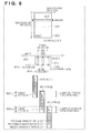
- FIG. 8 shows a state in which a scanner 810 is performing a reading operation on a sheet 800.
- the scanner 810 has a line shape longer than the width (paper width) in the main scanning direction of a sheet 800, and is capable of reading one line of image data at once. Accordingly, by the scanner 810 scanning or by the sheet 800 being fed in the sub-scanning direction of the sheet 800, it is possible to capture an image of the entire sheet 800.
- FIG. 8 shows an enlarged view of a cross-section 805 of the sheet 800.
- the scanner 810 is configured with three line-shaped sensors 812, 814, and 816, with each sensor having a specific wavelength sensitivity corresponding respectively to a first color, a second color, and a third color, and each sensor reading image data of the corresponding color (plane).
- the respective sensors 812, 814, and 816 that constitute the scanner 810 cannot be physically disposed at the same position, so in the reading position of each sensor (each color) at a particular time, there is always a shift of several pixels, shown as a reading position shift 820 in FIG. 8 . Accordingly, when performing correction of read image data of the band area from one particular time to another particular time, it is necessary to consider that amount of that shift.
- the height of the band area is set in order to eliminate the influence of the reading position shift 820 of each color.
- the lower portion of FIG. 8 shows the relationship between band areas and processing areas in the second embodiment. According to FIG. 8 , it is seen that the band area height is set such that the processing range of each color in each band area shifts by the same amount as the reading position shift 820.
- Each band area has an overlapping area like in the above first embodiment, and as described with reference to FIG. 5 , the overlapping area is determined according to the processing range of each color in the band. That is, according to the second embodiment, the number of upper end overlapping pixels and the number of lower end overlapping pixels, and the processing range of each color (plane), are determined according to the reading position shift 820 of each color in the above scanner 810.
- the band area height is set according to the amount of position shift.
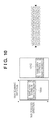
- FIG. 9 an exemplary dot-sequential data structure to be processed is shown in FIG. 9 , with reference numeral 450 denoting all image data.
- reference numeral 460 denotes 32-byte access unit data
- reference numeral 470 eight pixels of data are packed within the access unit data 460.
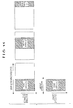
- the band area length direction can be set to match the sub-scanning direction of the image data. For example, as shown in the upper portion of FIG. 11 , when band areas have been divided in the main scanning direction of the image data, the length direction of each band area becomes the sub-scanning direction of the image data, as shown in the lower portion of FIG. 11 .
- the area of the pixels included in the 32-byte access unit data 460 in the image data structure shown in FIG. 9 to one pixel in the main scanning direction and eight pixels in the sub-scanning direction, it is possible to execute the band processing in the above first and second embodiments.
- the image processing in the above first and second embodiments there is not a dependency between band areas; the image processing can be executed independently for each band area. Accordingly, when band heights have been established in advance for a plurality of band areas, it is not necessary to perform image processing successively for each band area, so image processing can be accelerated by performing distributed parallel processing for each band area. Further, by developing the plurality of band areas for which the band height has been established in a plurality of processors and a memory possessed by these processors, it is of course possible in each processor to execute error diffusion and image processing such as sensor device correction and trapping.
- aspects of the present invention can also be realized by a computer of a system or apparatus (or devices such as a CPU or MPU) that reads out and executes a program recorded on a memory device to perform the functions of the above-described embodiment(s), and by a method, the steps of which are performed by a computer of a system or apparatus by, for example, reading out and executing a program recorded on a memory device to perform the functions of the above-described embodiment(s).
- the program is provided to the computer for example via a network or from a recording medium of various types serving as the memory device (e.g., computer-readable medium). While the present invention has been described with reference to exemplary embodiments, it is to be understood that the invention is not limited to the disclosed exemplary embodiments but by the scope of the following claims.
Landscapes
- Engineering & Computer Science (AREA)
- Multimedia (AREA)
- Signal Processing (AREA)
- Image Processing (AREA)
- Editing Of Facsimile Originals (AREA)
Claims (8)
- Appareil de traitement d'image destiné à effectuer un traitement d'image sur des données d'image constituées d'une pluralité de plans de couleur (512, 514, 516, 518), comprenant :un moyen destiné à obtenir, à partir des données d'image, une zone de bande (500, 510, 520) telle que la zone de bande (500, 510, 520) possède au moins une zone en chevauchement avec une zone de bande adjacente ;un moyen (150) de traitement d'image configuré pour effectuer le traitement d'image à l'intérieur de la zone de bande sur des zones de traitement distinctes pour chacun des plans de couleur (512, 514, 516, 518),dans lequel le traitement de bordures des zones de traitement diffère entre au moins deux plans de couleur parmi la pluralité de plans de couleur (512, 514, 516, 518).
- Appareil selon la revendication 1, dans lequel le moyen (150) de traitement d'image est en outre configuré pour :balayer la zone de bande (500, 510, 520) dans la direction du petit côté de la zone de bande (500, 510, 520) pour déterminer un pixel auquel on s'intéresse ; eten ce qui concerne le pixel auquel on s'intéresse à l'intérieur de la zone de bande (500, 510, 520), effectuer un calcul en se référant à un résultat de calcul pour un pixel pour lequel le traitement a déjà été effectué à l'intérieur d'une zone voisine.
- Appareil selon la revendication 2, dans lequel :le moyen de traitement d'image possède un moyen (660) formant mémoire tampon configuré pour conserver un résultat de calcul pour le pixel auquel on s'intéresse, etle moyen (660) formant mémoire tampon est capable de conserver les résultats de calcul pour au moins le nombre de pixels dans la direction du petit côté de la zone de bande (500, 510, 520).
- Appareil selon la revendication 3, dans lequel le moyen (150) de traitement d'image est en outre configuré pour effectuer une diffusion d'erreur pour le pixel auquel on s'intéresse, et pour conserver, dans le moyen (660) formant mémoire tampon, une erreur de quantification pour le pixel auquel on s'intéresse.
- Appareil selon la revendication 2, comprenant en outre un moyen (120) de lecture configuré pour obtenir les données d'image en lisant un original (110) en utilisant une pluralité de capteurs (126) qui correspondent respectivement à une pluralité de couleurs,
dans lequel la zone de traitement dans la direction du petit côté de la zone de bande (500, 510, 520) de chaque plan de couleur (512, 514, 516, 518) du moyen de traitement d'image est fixée de façon qu'une différence entre les zones de traitement des plans de couleur (512, 514, 516, 518) soit égale à une différence des positions de lecture des capteurs qui correspondent aux couleurs respectives. - Appareil selon la revendication 1, dans lequel le moyen (150) de traitement d'image est en outre configuré pour effectuer le traitement d'image pour la pluralité de zones de bande (500, 510, 520) en parallèle pour chaque zone de bande (500, 510, 520).
- Procédé de traitement d'image destiné à effectuer un traitement d'image sur des données d'image constituées d'une pluralité de plans de couleur (512, 514, 516, 518), comprenant :l'obtention, à partir des données d'image, d'une zone de bande (500, 510, 520) telle que la zone de bande (500, 510, 520) possède au moins une zone en chevauchement avec une zone de bande adjacente ;l'exécution du traitement d'image à l'intérieur de la zone de bande sur des zones de traitement distinctes pour chacun des plans de couleur (512, 514, 516, 518),dans lequel le traitement de bordures des zones de traitement diffère entre au moins deux plans de couleur parmi la pluralité de plans de couleur (512, 514, 516, 518).
- Programme mémorisé dans une mémoire lisible informatiquement (104, 106, 108) destiné à amener un processeur (100) à mettre en oeuvre le procédé de traitement d'image selon la revendication 7, lorsque le processeur (100) exécute le programme.
Applications Claiming Priority (1)
| Application Number | Priority Date | Filing Date | Title |
|---|---|---|---|
| JP2010034104A JP5584490B2 (ja) | 2010-02-18 | 2010-02-18 | 画像処理装置、画像処理方法およびプログラム |
Publications (3)
| Publication Number | Publication Date |
|---|---|
| EP2362632A2 EP2362632A2 (fr) | 2011-08-31 |
| EP2362632A3 EP2362632A3 (fr) | 2012-09-12 |
| EP2362632B1 true EP2362632B1 (fr) | 2015-03-18 |
Family
ID=43911611
Family Applications (1)
| Application Number | Title | Priority Date | Filing Date |
|---|---|---|---|
| EP11150691.1A Not-in-force EP2362632B1 (fr) | 2010-02-18 | 2011-01-12 | Appareil et procédé de traitement d'images |
Country Status (4)
| Country | Link |
|---|---|
| US (1) | US8520948B2 (fr) |
| EP (1) | EP2362632B1 (fr) |
| JP (1) | JP5584490B2 (fr) |
| CN (1) | CN102196149B (fr) |
Families Citing this family (11)
| Publication number | Priority date | Publication date | Assignee | Title |
|---|---|---|---|---|
| US20120218432A1 (en) * | 2011-02-28 | 2012-08-30 | Sony Corporation | Recursive adaptive intra smoothing for video coding |
| JP5955109B2 (ja) * | 2012-06-05 | 2016-07-20 | キヤノン株式会社 | 画像処理方法及び画像処理装置 |
| US9900459B2 (en) * | 2014-01-31 | 2018-02-20 | Kyocera Document Solutions Inc. | Image reading device |
| JP6035291B2 (ja) * | 2014-07-31 | 2016-11-30 | 京セラドキュメントソリューションズ株式会社 | ステッピングモーター駆動装置及び画像形成装置 |
| JP6706985B2 (ja) | 2015-08-06 | 2020-06-10 | キヤノン株式会社 | 画像処理装置およびその制御方法 |
| EP3128480B1 (fr) * | 2015-08-06 | 2018-06-27 | Canon Kabushiki Kaisha | Appareil de traitement d'image et procédé de commande associé |
| KR20190014777A (ko) * | 2017-08-03 | 2019-02-13 | 에스케이하이닉스 주식회사 | 이미지 신호 처리 시스템 및 방법 |
| CN110365865B (zh) * | 2018-03-26 | 2021-07-20 | 奇景光电股份有限公司 | 影像处理装置 |
| CN115503344B (zh) * | 2021-06-23 | 2024-03-22 | 森大(深圳)技术有限公司 | 驻留式图像打印方法、装置、设备及存储介质 |
| US12075016B1 (en) | 2023-12-11 | 2024-08-27 | Ricoh Company, Ltd. | Reordered multibit halftone processing with a threshold array |
| JP2026005397A (ja) * | 2024-06-27 | 2026-01-16 | キヤノン株式会社 | 画像処理方法、画像処理装置、及びプログラム |
Family Cites Families (13)
| Publication number | Priority date | Publication date | Assignee | Title |
|---|---|---|---|---|
| US5841145A (en) * | 1995-03-03 | 1998-11-24 | Fujitsu Limited | Method of and system for exposing pattern on object by charged particle beam |
| US5847721A (en) * | 1995-03-06 | 1998-12-08 | Canon Kabushiki Kaisha | Recording apparatus and method |
| US6587158B1 (en) | 1998-07-23 | 2003-07-01 | Dvdo, Inc. | Method and apparatus for reducing on-chip memory in vertical video processing |
| US6788432B1 (en) * | 1998-09-09 | 2004-09-07 | Hewlett-Packard Development Company, L.P. | Optimal-size and nozzle-modulated printmasks for use in incremental printing |
| JP3678051B2 (ja) | 1999-04-27 | 2005-08-03 | セイコーエプソン株式会社 | 画像形成装置、隠しパターン埋め込み方法及びプログラムを記録した記録媒体 |
| US6801636B2 (en) * | 2000-01-31 | 2004-10-05 | Canon Kabushiki Kaisha | Image processing apparatus and method, and storage medium |
| JPWO2002049341A1 (ja) * | 2000-12-11 | 2004-04-15 | 富士通株式会社 | 画像処理方法及び画像処理装置並びに記録媒体 |
| JP4594042B2 (ja) | 2004-11-12 | 2010-12-08 | キヤノン株式会社 | 画像処理方法、画像処理装置、及びコンピュータプログラム |
| JP5038763B2 (ja) * | 2006-04-04 | 2012-10-03 | 株式会社リコー | インクジェット記録装置と画像処理方法、画像処理制御プログラムと記録媒体および高浸透性顔料インク |
| JP5522890B2 (ja) | 2007-07-31 | 2014-06-18 | キヤノン株式会社 | 画像処理装置及び方法 |
| CN101222636B (zh) | 2008-01-24 | 2011-05-11 | 杭州华三通信技术有限公司 | 图像编解码方法和图像编解码装置 |
| JP4991640B2 (ja) | 2008-06-13 | 2012-08-01 | 京セラドキュメントソリューションズ株式会社 | 画像形成装置、画像処理方法及び画像処理プログラム |
| JP5222227B2 (ja) | 2009-05-22 | 2013-06-26 | キヤノン株式会社 | 画像処理方法、画像処理装置およびプログラム |
-
2010
- 2010-02-18 JP JP2010034104A patent/JP5584490B2/ja not_active Expired - Fee Related
-
2011
- 2011-01-12 EP EP11150691.1A patent/EP2362632B1/fr not_active Not-in-force
- 2011-01-21 US US13/011,248 patent/US8520948B2/en not_active Expired - Fee Related
- 2011-02-15 CN CN201110038935.5A patent/CN102196149B/zh not_active Expired - Fee Related
Also Published As
| Publication number | Publication date |
|---|---|
| US8520948B2 (en) | 2013-08-27 |
| EP2362632A2 (fr) | 2011-08-31 |
| JP5584490B2 (ja) | 2014-09-03 |
| US20110200253A1 (en) | 2011-08-18 |
| EP2362632A3 (fr) | 2012-09-12 |
| JP2011172027A (ja) | 2011-09-01 |
| CN102196149A (zh) | 2011-09-21 |
| CN102196149B (zh) | 2014-04-16 |
Similar Documents
| Publication | Publication Date | Title |
|---|---|---|
| US8520948B2 (en) | Image processing apparatus and image processing method | |
| US10027848B2 (en) | Image processing apparatus and control method for applying spatial filters to images | |
| US8477383B2 (en) | Processing based on command and register | |
| JP4279384B2 (ja) | カラーフィルタ画像信号生成方法 | |
| US8169656B2 (en) | Image processing devices and methods for resizing an original image therefor | |
| US9531911B2 (en) | Data processing apparatus, data processing method and storage medium for storing image data | |
| US9786250B2 (en) | Control apparatus, image processing apparatus, control method, and non-transitory computer-readable storage medium | |
| US9569703B2 (en) | Data transfer apparatus and method thereof | |
| JP4594042B2 (ja) | 画像処理方法、画像処理装置、及びコンピュータプログラム | |
| US8379998B2 (en) | Image processing apparatus and method | |
| US9055253B2 (en) | Method, apparatus, and medium acquiring band-area height on the basis of transfer amount and transfer unit of partial image data of the band area | |
| JP5182587B2 (ja) | 画像処理装置および画像処理方法 | |
| US20070058177A1 (en) | Image processing apparatus and image processing method | |
| JP2006213014A (ja) | 画像出力装置 | |
| US8416469B2 (en) | Image processing apparatus, image processing method and computer program | |
| US20050285871A1 (en) | Image-processing circuit, electronic apparatus, and method for processing image | |
| JP4753253B2 (ja) | 画像処理装置 | |
| JP4328608B2 (ja) | 画像処理装置、方法、プログラム及び記憶媒体 | |
| JP6808712B2 (ja) | 画像処理装置及びその制御方法、並びに、プログラム | |
| JP6489911B2 (ja) | 画像処理装置及びその制御方法 | |
| JP5597272B2 (ja) | 演算方法、演算装置、画像処理装置およびプログラム | |
| JP6562756B2 (ja) | 画像処理装置およびその制御方法 | |
| JP2011049893A (ja) | 画像処理装置および画像形成装置 | |
| EP2219363A1 (fr) | Système et procédé de traitement d'image numérique | |
| JPH0918715A (ja) | 画像処理方法 |
Legal Events
| Date | Code | Title | Description |
|---|---|---|---|
| PUAI | Public reference made under article 153(3) epc to a published international application that has entered the european phase |
Free format text: ORIGINAL CODE: 0009012 |
|
| AK | Designated contracting states |
Kind code of ref document: A2 Designated state(s): AL AT BE BG CH CY CZ DE DK EE ES FI FR GB GR HR HU IE IS IT LI LT LU LV MC MK MT NL NO PL PT RO RS SE SI SK SM TR |
|
| AX | Request for extension of the european patent |
Extension state: BA ME |
|
| PUAL | Search report despatched |
Free format text: ORIGINAL CODE: 0009013 |
|
| AK | Designated contracting states |
Kind code of ref document: A3 Designated state(s): AL AT BE BG CH CY CZ DE DK EE ES FI FR GB GR HR HU IE IS IT LI LT LU LV MC MK MT NL NO PL PT RO RS SE SI SK SM TR |
|
| AX | Request for extension of the european patent |
Extension state: BA ME |
|
| RIC1 | Information provided on ipc code assigned before grant |
Ipc: H04N 1/46 20060101AFI20120806BHEP |
|
| 17P | Request for examination filed |
Effective date: 20130312 |
|
| 17Q | First examination report despatched |
Effective date: 20130709 |
|
| GRAP | Despatch of communication of intention to grant a patent |
Free format text: ORIGINAL CODE: EPIDOSNIGR1 |
|
| INTG | Intention to grant announced |
Effective date: 20140923 |
|
| GRAS | Grant fee paid |
Free format text: ORIGINAL CODE: EPIDOSNIGR3 |
|
| GRAA | (expected) grant |
Free format text: ORIGINAL CODE: 0009210 |
|
| AK | Designated contracting states |
Kind code of ref document: B1 Designated state(s): AL AT BE BG CH CY CZ DE DK EE ES FI FR GB GR HR HU IE IS IT LI LT LU LV MC MK MT NL NO PL PT RO RS SE SI SK SM TR |
|
| REG | Reference to a national code |
Ref country code: GB Ref legal event code: FG4D |
|
| REG | Reference to a national code |
Ref country code: CH Ref legal event code: EP |
|
| REG | Reference to a national code |
Ref country code: IE Ref legal event code: FG4D |
|
| REG | Reference to a national code |
Ref country code: AT Ref legal event code: REF Ref document number: 717189 Country of ref document: AT Kind code of ref document: T Effective date: 20150415 |
|
| REG | Reference to a national code |
Ref country code: DE Ref legal event code: R096 Ref document number: 602011014713 Country of ref document: DE Effective date: 20150430 |
|
| REG | Reference to a national code |
Ref country code: NL Ref legal event code: VDEP Effective date: 20150318 |
|
| REG | Reference to a national code |
Ref country code: NL Ref legal event code: VDEP Effective date: 20150318 |
|
| PG25 | Lapsed in a contracting state [announced via postgrant information from national office to epo] |
Ref country code: LT Free format text: LAPSE BECAUSE OF FAILURE TO SUBMIT A TRANSLATION OF THE DESCRIPTION OR TO PAY THE FEE WITHIN THE PRESCRIBED TIME-LIMIT Effective date: 20150318 Ref country code: NO Free format text: LAPSE BECAUSE OF FAILURE TO SUBMIT A TRANSLATION OF THE DESCRIPTION OR TO PAY THE FEE WITHIN THE PRESCRIBED TIME-LIMIT Effective date: 20150618 Ref country code: FI Free format text: LAPSE BECAUSE OF FAILURE TO SUBMIT A TRANSLATION OF THE DESCRIPTION OR TO PAY THE FEE WITHIN THE PRESCRIBED TIME-LIMIT Effective date: 20150318 Ref country code: SE Free format text: LAPSE BECAUSE OF FAILURE TO SUBMIT A TRANSLATION OF THE DESCRIPTION OR TO PAY THE FEE WITHIN THE PRESCRIBED TIME-LIMIT Effective date: 20150318 Ref country code: HR Free format text: LAPSE BECAUSE OF FAILURE TO SUBMIT A TRANSLATION OF THE DESCRIPTION OR TO PAY THE FEE WITHIN THE PRESCRIBED TIME-LIMIT Effective date: 20150318 |
|
| REG | Reference to a national code |
Ref country code: AT Ref legal event code: MK05 Ref document number: 717189 Country of ref document: AT Kind code of ref document: T Effective date: 20150318 |
|
| REG | Reference to a national code |
Ref country code: LT Ref legal event code: MG4D |
|
| PG25 | Lapsed in a contracting state [announced via postgrant information from national office to epo] |
Ref country code: GR Free format text: LAPSE BECAUSE OF FAILURE TO SUBMIT A TRANSLATION OF THE DESCRIPTION OR TO PAY THE FEE WITHIN THE PRESCRIBED TIME-LIMIT Effective date: 20150619 Ref country code: LV Free format text: LAPSE BECAUSE OF FAILURE TO SUBMIT A TRANSLATION OF THE DESCRIPTION OR TO PAY THE FEE WITHIN THE PRESCRIBED TIME-LIMIT Effective date: 20150318 Ref country code: RS Free format text: LAPSE BECAUSE OF FAILURE TO SUBMIT A TRANSLATION OF THE DESCRIPTION OR TO PAY THE FEE WITHIN THE PRESCRIBED TIME-LIMIT Effective date: 20150318 |
|
| PG25 | Lapsed in a contracting state [announced via postgrant information from national office to epo] |
Ref country code: NL Free format text: LAPSE BECAUSE OF FAILURE TO SUBMIT A TRANSLATION OF THE DESCRIPTION OR TO PAY THE FEE WITHIN THE PRESCRIBED TIME-LIMIT Effective date: 20150318 |
|
| PG25 | Lapsed in a contracting state [announced via postgrant information from national office to epo] |
Ref country code: SK Free format text: LAPSE BECAUSE OF FAILURE TO SUBMIT A TRANSLATION OF THE DESCRIPTION OR TO PAY THE FEE WITHIN THE PRESCRIBED TIME-LIMIT Effective date: 20150318 Ref country code: RO Free format text: LAPSE BECAUSE OF FAILURE TO SUBMIT A TRANSLATION OF THE DESCRIPTION OR TO PAY THE FEE WITHIN THE PRESCRIBED TIME-LIMIT Effective date: 20150318 Ref country code: ES Free format text: LAPSE BECAUSE OF FAILURE TO SUBMIT A TRANSLATION OF THE DESCRIPTION OR TO PAY THE FEE WITHIN THE PRESCRIBED TIME-LIMIT Effective date: 20150318 Ref country code: CZ Free format text: LAPSE BECAUSE OF FAILURE TO SUBMIT A TRANSLATION OF THE DESCRIPTION OR TO PAY THE FEE WITHIN THE PRESCRIBED TIME-LIMIT Effective date: 20150318 Ref country code: EE Free format text: LAPSE BECAUSE OF FAILURE TO SUBMIT A TRANSLATION OF THE DESCRIPTION OR TO PAY THE FEE WITHIN THE PRESCRIBED TIME-LIMIT Effective date: 20150318 Ref country code: PT Free format text: LAPSE BECAUSE OF FAILURE TO SUBMIT A TRANSLATION OF THE DESCRIPTION OR TO PAY THE FEE WITHIN THE PRESCRIBED TIME-LIMIT Effective date: 20150720 |
|
| PG25 | Lapsed in a contracting state [announced via postgrant information from national office to epo] |
Ref country code: AT Free format text: LAPSE BECAUSE OF FAILURE TO SUBMIT A TRANSLATION OF THE DESCRIPTION OR TO PAY THE FEE WITHIN THE PRESCRIBED TIME-LIMIT Effective date: 20150318 Ref country code: IS Free format text: LAPSE BECAUSE OF FAILURE TO SUBMIT A TRANSLATION OF THE DESCRIPTION OR TO PAY THE FEE WITHIN THE PRESCRIBED TIME-LIMIT Effective date: 20150718 Ref country code: PL Free format text: LAPSE BECAUSE OF FAILURE TO SUBMIT A TRANSLATION OF THE DESCRIPTION OR TO PAY THE FEE WITHIN THE PRESCRIBED TIME-LIMIT Effective date: 20150318 |
|
| REG | Reference to a national code |
Ref country code: DE Ref legal event code: R097 Ref document number: 602011014713 Country of ref document: DE |
|
| PG25 | Lapsed in a contracting state [announced via postgrant information from national office to epo] |
Ref country code: IT Free format text: LAPSE BECAUSE OF FAILURE TO SUBMIT A TRANSLATION OF THE DESCRIPTION OR TO PAY THE FEE WITHIN THE PRESCRIBED TIME-LIMIT Effective date: 20150318 |
|
| PLBE | No opposition filed within time limit |
Free format text: ORIGINAL CODE: 0009261 |
|
| STAA | Information on the status of an ep patent application or granted ep patent |
Free format text: STATUS: NO OPPOSITION FILED WITHIN TIME LIMIT |
|
| PG25 | Lapsed in a contracting state [announced via postgrant information from national office to epo] |
Ref country code: DK Free format text: LAPSE BECAUSE OF FAILURE TO SUBMIT A TRANSLATION OF THE DESCRIPTION OR TO PAY THE FEE WITHIN THE PRESCRIBED TIME-LIMIT Effective date: 20150318 |
|
| 26N | No opposition filed |
Effective date: 20151221 |
|
| PG25 | Lapsed in a contracting state [announced via postgrant information from national office to epo] |
Ref country code: SI Free format text: LAPSE BECAUSE OF FAILURE TO SUBMIT A TRANSLATION OF THE DESCRIPTION OR TO PAY THE FEE WITHIN THE PRESCRIBED TIME-LIMIT Effective date: 20150318 |
|
| PG25 | Lapsed in a contracting state [announced via postgrant information from national office to epo] |
Ref country code: BE Free format text: LAPSE BECAUSE OF NON-PAYMENT OF DUE FEES Effective date: 20160131 |
|
| PG25 | Lapsed in a contracting state [announced via postgrant information from national office to epo] |
Ref country code: LU Free format text: LAPSE BECAUSE OF FAILURE TO SUBMIT A TRANSLATION OF THE DESCRIPTION OR TO PAY THE FEE WITHIN THE PRESCRIBED TIME-LIMIT Effective date: 20160112 Ref country code: BE Free format text: LAPSE BECAUSE OF FAILURE TO SUBMIT A TRANSLATION OF THE DESCRIPTION OR TO PAY THE FEE WITHIN THE PRESCRIBED TIME-LIMIT Effective date: 20150318 |
|
| REG | Reference to a national code |
Ref country code: CH Ref legal event code: PL |
|
| PG25 | Lapsed in a contracting state [announced via postgrant information from national office to epo] |
Ref country code: MC Free format text: LAPSE BECAUSE OF FAILURE TO SUBMIT A TRANSLATION OF THE DESCRIPTION OR TO PAY THE FEE WITHIN THE PRESCRIBED TIME-LIMIT Effective date: 20150318 |
|
| REG | Reference to a national code |
Ref country code: FR Ref legal event code: ST Effective date: 20160930 |
|
| PG25 | Lapsed in a contracting state [announced via postgrant information from national office to epo] |
Ref country code: LI Free format text: LAPSE BECAUSE OF NON-PAYMENT OF DUE FEES Effective date: 20160131 Ref country code: CH Free format text: LAPSE BECAUSE OF NON-PAYMENT OF DUE FEES Effective date: 20160131 |
|
| REG | Reference to a national code |
Ref country code: IE Ref legal event code: MM4A |
|
| PG25 | Lapsed in a contracting state [announced via postgrant information from national office to epo] |
Ref country code: FR Free format text: LAPSE BECAUSE OF NON-PAYMENT OF DUE FEES Effective date: 20160201 |
|
| PG25 | Lapsed in a contracting state [announced via postgrant information from national office to epo] |
Ref country code: IE Free format text: LAPSE BECAUSE OF NON-PAYMENT OF DUE FEES Effective date: 20160112 |
|
| PG25 | Lapsed in a contracting state [announced via postgrant information from national office to epo] |
Ref country code: MT Free format text: LAPSE BECAUSE OF FAILURE TO SUBMIT A TRANSLATION OF THE DESCRIPTION OR TO PAY THE FEE WITHIN THE PRESCRIBED TIME-LIMIT Effective date: 20150318 |
|
| PG25 | Lapsed in a contracting state [announced via postgrant information from national office to epo] |
Ref country code: CY Free format text: LAPSE BECAUSE OF FAILURE TO SUBMIT A TRANSLATION OF THE DESCRIPTION OR TO PAY THE FEE WITHIN THE PRESCRIBED TIME-LIMIT Effective date: 20150318 Ref country code: SM Free format text: LAPSE BECAUSE OF FAILURE TO SUBMIT A TRANSLATION OF THE DESCRIPTION OR TO PAY THE FEE WITHIN THE PRESCRIBED TIME-LIMIT Effective date: 20150318 Ref country code: HU Free format text: LAPSE BECAUSE OF FAILURE TO SUBMIT A TRANSLATION OF THE DESCRIPTION OR TO PAY THE FEE WITHIN THE PRESCRIBED TIME-LIMIT; INVALID AB INITIO Effective date: 20110112 |
|
| PG25 | Lapsed in a contracting state [announced via postgrant information from national office to epo] |
Ref country code: TR Free format text: LAPSE BECAUSE OF FAILURE TO SUBMIT A TRANSLATION OF THE DESCRIPTION OR TO PAY THE FEE WITHIN THE PRESCRIBED TIME-LIMIT Effective date: 20150318 Ref country code: MK Free format text: LAPSE BECAUSE OF FAILURE TO SUBMIT A TRANSLATION OF THE DESCRIPTION OR TO PAY THE FEE WITHIN THE PRESCRIBED TIME-LIMIT Effective date: 20150318 Ref country code: MT Free format text: LAPSE BECAUSE OF FAILURE TO SUBMIT A TRANSLATION OF THE DESCRIPTION OR TO PAY THE FEE WITHIN THE PRESCRIBED TIME-LIMIT Effective date: 20160131 |
|
| PG25 | Lapsed in a contracting state [announced via postgrant information from national office to epo] |
Ref country code: BG Free format text: LAPSE BECAUSE OF FAILURE TO SUBMIT A TRANSLATION OF THE DESCRIPTION OR TO PAY THE FEE WITHIN THE PRESCRIBED TIME-LIMIT Effective date: 20150318 |
|
| PG25 | Lapsed in a contracting state [announced via postgrant information from national office to epo] |
Ref country code: AL Free format text: LAPSE BECAUSE OF FAILURE TO SUBMIT A TRANSLATION OF THE DESCRIPTION OR TO PAY THE FEE WITHIN THE PRESCRIBED TIME-LIMIT Effective date: 20150318 |
|
| PGFP | Annual fee paid to national office [announced via postgrant information from national office to epo] |
Ref country code: GB Payment date: 20231219 Year of fee payment: 14 |
|
| PGFP | Annual fee paid to national office [announced via postgrant information from national office to epo] |
Ref country code: DE Payment date: 20231219 Year of fee payment: 14 |
|
| REG | Reference to a national code |
Ref country code: DE Ref legal event code: R119 Ref document number: 602011014713 Country of ref document: DE |
|
| GBPC | Gb: european patent ceased through non-payment of renewal fee |
Effective date: 20250112 |
|
| PG25 | Lapsed in a contracting state [announced via postgrant information from national office to epo] |
Ref country code: DE Free format text: LAPSE BECAUSE OF NON-PAYMENT OF DUE FEES Effective date: 20250801 |
|
| PG25 | Lapsed in a contracting state [announced via postgrant information from national office to epo] |
Ref country code: GB Free format text: LAPSE BECAUSE OF NON-PAYMENT OF DUE FEES Effective date: 20250112 |