EP2363684A1 - Cellule de calibrage - Google Patents
Cellule de calibrage Download PDFInfo
- Publication number
- EP2363684A1 EP2363684A1 EP10001391A EP10001391A EP2363684A1 EP 2363684 A1 EP2363684 A1 EP 2363684A1 EP 10001391 A EP10001391 A EP 10001391A EP 10001391 A EP10001391 A EP 10001391A EP 2363684 A1 EP2363684 A1 EP 2363684A1
- Authority
- EP
- European Patent Office
- Prior art keywords
- layer
- substrate
- reflective layer
- calibration cell
- reflective
- Prior art date
- Legal status (The legal status is an assumption and is not a legal conclusion. Google has not performed a legal analysis and makes no representation as to the accuracy of the status listed.)
- Granted
Links
Images


Classifications
-
- G—PHYSICS
- G01—MEASURING; TESTING
- G01B—MEASURING LENGTH, THICKNESS OR SIMILAR LINEAR DIMENSIONS; MEASURING ANGLES; MEASURING AREAS; MEASURING IRREGULARITIES OF SURFACES OR CONTOURS
- G01B3/00—Measuring instruments characterised by the use of mechanical techniques
- G01B3/30—Bars, blocks, or strips in which the distance between a pair of faces is fixed, although it may be preadjustable, e.g. end measure, feeler strip
-
- G—PHYSICS
- G01—MEASURING; TESTING
- G01B—MEASURING LENGTH, THICKNESS OR SIMILAR LINEAR DIMENSIONS; MEASURING ANGLES; MEASURING AREAS; MEASURING IRREGULARITIES OF SURFACES OR CONTOURS
- G01B21/00—Measuring arrangements or details thereof, where the measuring technique is not covered by the other groups of this subclass, unspecified or not relevant
- G01B21/02—Measuring arrangements or details thereof, where the measuring technique is not covered by the other groups of this subclass, unspecified or not relevant for measuring length, width, or thickness
- G01B21/04—Measuring arrangements or details thereof, where the measuring technique is not covered by the other groups of this subclass, unspecified or not relevant for measuring length, width, or thickness by measuring coordinates of points
- G01B21/042—Calibration or calibration artifacts
-
- G—PHYSICS
- G01—MEASURING; TESTING
- G01N—INVESTIGATING OR ANALYSING MATERIALS BY DETERMINING THEIR CHEMICAL OR PHYSICAL PROPERTIES
- G01N21/00—Investigating or analysing materials by the use of optical means, i.e. using sub-millimetre waves, infrared, visible or ultraviolet light
- G01N21/17—Systems in which incident light is modified in accordance with the properties of the material investigated
- G01N21/25—Colour; Spectral properties, i.e. comparison of effect of material on the light at two or more different wavelengths or wavelength bands
- G01N21/27—Colour; Spectral properties, i.e. comparison of effect of material on the light at two or more different wavelengths or wavelength bands using photo-electric detection ; circuits for computing concentration
- G01N21/274—Calibration, base line adjustment, drift correction
- G01N21/278—Constitution of standards
-
- G—PHYSICS
- G01—MEASURING; TESTING
- G01N—INVESTIGATING OR ANALYSING MATERIALS BY DETERMINING THEIR CHEMICAL OR PHYSICAL PROPERTIES
- G01N21/00—Investigating or analysing materials by the use of optical means, i.e. using sub-millimetre waves, infrared, visible or ultraviolet light
- G01N21/17—Systems in which incident light is modified in accordance with the properties of the material investigated
- G01N21/55—Specular reflectivity
-
- G—PHYSICS
- G01—MEASURING; TESTING
- G01N—INVESTIGATING OR ANALYSING MATERIALS BY DETERMINING THEIR CHEMICAL OR PHYSICAL PROPERTIES
- G01N21/00—Investigating or analysing materials by the use of optical means, i.e. using sub-millimetre waves, infrared, visible or ultraviolet light
- G01N21/17—Systems in which incident light is modified in accordance with the properties of the material investigated
- G01N21/59—Transmissivity
Definitions
- the invention relates to a method for producing a sample for optical calibration measurements and measurements for verifying measurement accuracy, and to such a sample, in particular for calibrating and / or verifying imaging measuring devices for determining geometric dimensions, as used, for example, in the field of manufacturing solar cells ,
- measured samples are usually used beforehand, preferably by means of another measuring device or another measuring method, and measured by the measuring device to be calibrated or by the measuring method to be calibrated, in order to match the measured values determined in the calibration with the previously known measured values to reach.
- a sample may be used whose exact dimensions are sufficiently well known due to the method of fabricating the sample.
- Such a previously known measurement sample is called a calibration sample.
- calibration samples are also needed and used to check whether the measurement results provided by a measuring device or measurement method are correct or within specified measurement tolerances. Such a check is also referred to as checking a measuring capability. In this case, it is determined whether the measuring device or the measuring method have the ability to correctly measure samples within the scope of a given measuring tolerance.
- calibration sample which is suitable for calibration measurements or control measurements for checking the measurement capability of a measuring device, which can determine both the geometric dimensions of the semiconductor substrate of a solar cell and a printing applied thereto, is hereinafter referred to as calibration sample.
- the object is achieved by a method for producing a calibration cell having the features of patent claim 1, a calibration cell having the features of patent claim 6, and a method for detecting a measuring capability having the features of patent claim 14.
- the invention is based on the idea of creating a calibration sample which is easy to reproducibly produce in terms of its geometric properties and, on the other hand, reflects the properties of a semiconductor component, in particular a solar cell, which are necessary for an imaging measurement as well as possible.
- a calibration cell comprises a transparent substrate having a side surface on which a highly structured structured reflective layer is applied, which reflects reflecting radiation transmitted through the transparent substrate, wherein the structure is formed such that the reflective layer has recesses on which the side surface is not is covered by the reflective layer, and a scattering layer which diffusely reflected in reflected light, wherein the scattering layer fills at least one of the recesses over the entire surface.
- a high-precision structured reflective layer defines both the lateral dimensions of the structures of the reflective layer and the lateral geometric dimensions of the recesses filling areas of the scattering layer, which are detectable when viewing the calibration cell through the transparent substrate.
- a method for producing a calibration cell thus comprises the steps of providing a transparent substrate, applying a highly precisely patterned reflective layer to a side surface of the substrate, wherein the structure formed in this case is configured so that the reflective layer has at least one recess, preferably a plurality of recesses, at or on which the side surface of the substrate is not covered with the reflective layer, and then applying a scattering layer, which diffusely reflected in incident light, wherein the at least one recess, preferably a plurality of recesses, are filled over the entire surface with the litter layer.
- the geometric contours of the structured reflecting layer are determined by viewing the calibration cell in transmitted light from the substrate side or imaging it in a spatially resolved manner.
- the specular layer is impermeable to radiation, for example light, so that the areas covered by the specular layer clearly stand out from the uncovered substrate, so that the contours of a contrast difference are easily and accurately determined. If the scattering layer is produced from a translucent material, the regions of the reflecting layer also stand out in the transmitted light against the substrate covered with the translucent scattering layer in the region of the recesses.
- the radiation used for example light in the visible range
- the radiation used reflects the radiation components incident on the specular sections of the structured specular layer in accordance with the laws of geometric optics. This makes it possible to achieve that this light is not detected in the spatially resolved imaging of the calibration cell.
- the reflecting areas are thus depicted as dark areas. Since the radiation impinging on the scattering layer is diffusely reflected, the recesses filled in over the entire area by the scattering layer can be clearly seen as bright areas in the spatially resolved image.
- the geometrical dimensions of the scattering regions are determined by the high-precision structuring of the reflecting regions, so that it is sufficient to structure the reflecting layer with high precision.
- a recess in the reflective layer, which is not completely enclosed by this, is filled voüflächig, provided that there is an imaginary degree extending through two points on the contour of the reflective layer defining the recess, which encloses a region of the recess together with the defining contour and this so enclosed area is completely filled.
- the geometric dimensions determined are compared with the previously known dimensions.
- geometrical imaging changes caused by viewing through the substrate may be taken into account.
- a particularly simple high-precision and reproducible structuring during the application of the reflecting layer can be achieved by using a mask.
- Masks can be produced very precisely with tolerances in the sub-micron range, for example by lithographic processes.
- the parts of the substrate layer are covered, to which the reflective layer should not be applied.
- materials such as chromium, molybdenum, gold, silver, or any other material that forms a specular surface on the substrate while being sufficiently opaque to transmitted light can be used.
- the Application can be carried out by means of any method, for example via vapor deposition, sputtering or the like.
- a substrate layer is particularly suitable a transparent material which has a low coefficient of thermal expansion.
- a transparent material which has a low coefficient of thermal expansion.
- quartz glass or borosilicate glass are suitable substrate materials, which furthermore have high mechanical stability.
- the diffuse reflective layer For the formation of the diffuse reflective layer, a variety of materials come into consideration.
- the application can be done by printing, vapor deposition or in a dipping process. Any method can be used. The only requirement is that the layer is applied so that at least one formed in the reflective layer recess is completely filled by the material of the litter layer.
- the scattering layer is designed to be translucent or is diffused, in particular diffusely in transmitted light.
- a contrast between the opaque mirrored layer and the scattering layer can be achieved in transmitted light.
- the measuring device delivers precise measured values for a known calibration sample, it is of great interest, for example in the field of solar cell production, to precisely measure the geometric outer contour.
- the reflecting layer is applied to the side surface of the substrate such that a peripheral edge strip of the substrate Side surface of the substrate remains uncovered by the reflective layer.
- the side surface thus has a peripheral edge area which is uncovered by the reflecting layer.
- the peripheral edge region is not covered by the scattering layer. This can be achieved, for example, by using, after the application of the reflecting layer for applying the scattering layer, a further mask which completely covers this edge area. Likewise, it is possible to apply a protective layer which completely covers this circumferential edge region, which is then removed again after application of the scattering layer.
- an induction layer is additionally applied to the scattering layer, which is detectable by means of inductively measuring sensors.
- an induction layer is thus made of a conductive material into which eddy currents are inducible.
- the person skilled in various metals and alloys are known which are suitable for this purpose.
- the reflective layer is usually designed in terms of their material thickness so that it is not reliably detected by inductively measuring sensors. Since the induction layer, when made of a metal or alloy, is opaque to transmitted light, it is suitably applied to the patterning of the specular layer.
- the contours of the reflecting layer intended for checking the measuring capability are not covered by material of the induction layer. Since it usually only depends on the external dimensions of the solar cell for a detection of the measurement capability with respect to the solar cell material at measuring devices, it is usually only necessary that the above-mentioned circumferential edge region is not covered by the induction layer. As a rule, a further edge region, which is larger in area than the peripheral edge region and completely covers it, is left free and is not covered by the induction layer. Again this can be done by the Use of a mask or applying a protective layer before applying the induction layer, wherein the protective layer is removed after application again. It will be understood by those skilled in the art that when using a mask or protective layer, they may each be the same for the application of the scattering layer and the induction layer.
- the lateral surface opposite the lateral surface provided with the reflective layer is provided with an antireflection coating in a preferred embodiment.
- an antireflection coating in a preferred embodiment.
- one or more antireflection layers can be applied or be.
- typical defects occurring in solar cells are reproduced. These may include, for example, edge breakouts, cracks, or stains on the print simulated by changes in the patterning of the specular layer or mechanical damage or manipulation of the applied layers.
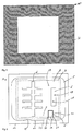
- Fig. 1 schematically is a calibration cell 1 as a sectional view along a section line AB to Fig. 2 shown.
- the calibrator cell 1 comprises a transparent substrate 2. This is extended flat perpendicular to the plane of the drawing.
- a transparent material are glasses or quartz glass, for example.
- the substrate has a side surface which is planar.
- the side surface 3 is preferably plane-parallel to an opposite side surface 4, which is also flat.
- a high-precision structured reflective layer 5 is applied on the side surface 3.
- the reflective layer 5 is made of, for example, chromium or tungsten. Any other materials may be used as long as radiation incident on the specular layer (5) by the substrate is mirrored thereto according to the laws of geometric optics.
- the reflective layer 5 has recesses 6.
- a scattering layer 7 is applied on the reflective layer 5 and on the side surface 3 of the substrate 2 in the region of the recesses 6. This is designed such that it diffusely reflects incident radiation in incident light.
- scattering layer is formed so that the scattering layer is at least translucent in transmitted light, preferably diffusely scatters.
- an induction layer 8 is additionally applied to the scattering layer 7. This is made of a material that interacts with an inductive measuring sensor. In particular, therefore, metallic materials which are applied in a sufficient layer thickness 9 are suitable.
- the induction layer is used by a number of measuring devices to trigger a measurement of the measuring device when inductive sensors provide a presence of the calibration cell in the detection range of the measuring device.
- Fig. 2 is a plan view of the calibration cell 1 after Fig. 1 represented, wherein the calibration cell through the substrate 2 and the anti-reflection layer 16 (see. Fig. 1 ) is looked at.
- the reflective layer 5 is applied to the substrate 2 in such a way that an edge region 10 remains uncovered circumferentially by the side surface 3. This edge area remains uncovered by the litter layer and the possibly present induction layer.
- the scattering layer 7 and the induction layer 8 each leave corresponding further, preferably wider edge regions 12 or 13, which are preferably wider than the edge region 10, uncovered around an outer contour 14 of the substrate 2.
- an outer contour visible in transmitted light is defined by the highly precisely structured reflective layer.
- An overlap of the edge region 10 by the scattering layer 7 would be tolerable, provided that it is translucent.
- the induction layer 8 must always be applied in such a way that it does not cover an outer contour 15 of the specular layer 5 to be measured.
- the high-precision structuring is achieved by covering the areas of the substrate layer with a mask, which should not be covered with the reflective layer.
- FIG Fig. 3 Schematically, such a mask 11 is in FIG Fig. 3 shown.
- Masks can be produced with a quality that is dimensional deviations of the structure defined by the mask of a given structure significantly smaller than the achievable measurement tolerances of the measuring devices used.
- reflective layers can be applied to substrate surfaces which, in terms of their dimensional stability, have deviations from the predefined structure below the dimensional tolerances of the measuring devices in the structuring.
- Fig. 4 is a further mask 11 'is shown, for example, for applying the litter layer 7 according to Fig. 1 and Fig. 2 is used, by the only the peripheral edge region 12 according to Fig. 1 and Fig. 2 is covered by a further cover 25.
- a similar mask 11 "with a further cover 26, through which the edge region 13 according to Fig. 1 and Fig. 2 is covered is in Fig. 5 shown and can when applying the induction layer 8 according to Fig. 1 and Fig. 2 be used.
- Fig. 6 is a calibration cell 1 similar to the after Fig. 1 shown, however, has defects.
- a contour modification 17 modeling an edge breakout is incorporated in the outer contour 15 of the reflecting layer 5.
- small areas 18 of the reflecting layer are additionally inserted in order to simulate stains in the printing.
- holes 27 may be introduced in the specular layer to mimic printing defects. Other imperfections can be reproduced by introducing scratches or deliberately introduced impurities into the individual layers, in particular the litter layer or the reflecting layer.
- FIG. 6 An imaginary straight line 19 extends through the points 20, 21 which lie on the contour 22 of the reflecting layer 5 which delimits the recess 6 ', enclosing the surrounding contour together with the contour 22 an area of the recess 6 ', which is filled over the entire area with the litter layer.
- the recess 6 ' is thus filled within the meaning of the invention also over the entire surface with the scattered view.
- the individual dimensions in particular the layer thicknesses of the substrate 2 in the Verfiältnis to the layer thicknesses of the reflective layer 5, the litter layer 7 and the induction layer 8, are not shown to scale.
- the substrate layer has a much greater layer thickness than the reflective layer 5, the diffusion layer 7 and the induction layer 8 and the antireflection layer 16.
Landscapes
- Physics & Mathematics (AREA)
- General Physics & Mathematics (AREA)
- Immunology (AREA)
- Pathology (AREA)
- Analytical Chemistry (AREA)
- Biochemistry (AREA)
- General Health & Medical Sciences (AREA)
- Life Sciences & Earth Sciences (AREA)
- Health & Medical Sciences (AREA)
- Chemical & Material Sciences (AREA)
- Engineering & Computer Science (AREA)
- Mathematical Physics (AREA)
- Theoretical Computer Science (AREA)
- Spectroscopy & Molecular Physics (AREA)
- Photovoltaic Devices (AREA)
- Length Measuring Devices By Optical Means (AREA)
Priority Applications (1)
| Application Number | Priority Date | Filing Date | Title |
|---|---|---|---|
| EP10001391.1A EP2363684B8 (fr) | 2010-02-10 | 2010-02-10 | Cellule de calibrage |
Applications Claiming Priority (1)
| Application Number | Priority Date | Filing Date | Title |
|---|---|---|---|
| EP10001391.1A EP2363684B8 (fr) | 2010-02-10 | 2010-02-10 | Cellule de calibrage |
Publications (3)
| Publication Number | Publication Date |
|---|---|
| EP2363684A1 true EP2363684A1 (fr) | 2011-09-07 |
| EP2363684B1 EP2363684B1 (fr) | 2020-04-22 |
| EP2363684B8 EP2363684B8 (fr) | 2020-06-10 |
Family
ID=42288576
Family Applications (1)
| Application Number | Title | Priority Date | Filing Date |
|---|---|---|---|
| EP10001391.1A Not-in-force EP2363684B8 (fr) | 2010-02-10 | 2010-02-10 | Cellule de calibrage |
Country Status (1)
| Country | Link |
|---|---|
| EP (1) | EP2363684B8 (fr) |
Cited By (2)
| Publication number | Priority date | Publication date | Assignee | Title |
|---|---|---|---|---|
| US11867630B1 (en) | 2022-08-09 | 2024-01-09 | Glasstech, Inc. | Fixture and method for optical alignment in a system for measuring a surface in contoured glass sheets |
| US12079980B2 (en) | 2018-07-24 | 2024-09-03 | Glasstech, Inc. | System and method for measuring a surface in contoured glass sheets |
Citations (6)
| Publication number | Priority date | Publication date | Assignee | Title |
|---|---|---|---|---|
| US6664535B1 (en) * | 2002-07-16 | 2003-12-16 | Mitutoyo Corporation | Scale structures and methods usable in an absolute position transducer |
| US20040227937A1 (en) * | 1997-06-25 | 2004-11-18 | Richardson Timothy M. | Test slide for microscopes and method for the production of such a slide |
| US20060183342A1 (en) | 2005-02-15 | 2006-08-17 | Eastman Kodak Company | Metal and metal oxide patterned device |
| EP1703273A1 (fr) * | 2005-03-18 | 2006-09-20 | BAM Bundesanstalt für Materialforschung und -prüfung | Dispositif multifonctionnel de calibrage et ensemble, tout comme son utilisation destinée à la caractérisation de systèmes luminescents |
| JP2007328038A (ja) * | 2006-06-06 | 2007-12-20 | Hitachi High-Technologies Corp | 顕微鏡用寸法校正試料 |
| DE102008007178A1 (de) | 2008-01-30 | 2009-08-06 | Carl Zeiss Microimaging Gmbh | Kalibriervorrichtung und Laser-Scanning-Mikroskop mit einer derartigen Kalibriervorrichtung |
-
2010
- 2010-02-10 EP EP10001391.1A patent/EP2363684B8/fr not_active Not-in-force
Patent Citations (6)
| Publication number | Priority date | Publication date | Assignee | Title |
|---|---|---|---|---|
| US20040227937A1 (en) * | 1997-06-25 | 2004-11-18 | Richardson Timothy M. | Test slide for microscopes and method for the production of such a slide |
| US6664535B1 (en) * | 2002-07-16 | 2003-12-16 | Mitutoyo Corporation | Scale structures and methods usable in an absolute position transducer |
| US20060183342A1 (en) | 2005-02-15 | 2006-08-17 | Eastman Kodak Company | Metal and metal oxide patterned device |
| EP1703273A1 (fr) * | 2005-03-18 | 2006-09-20 | BAM Bundesanstalt für Materialforschung und -prüfung | Dispositif multifonctionnel de calibrage et ensemble, tout comme son utilisation destinée à la caractérisation de systèmes luminescents |
| JP2007328038A (ja) * | 2006-06-06 | 2007-12-20 | Hitachi High-Technologies Corp | 顕微鏡用寸法校正試料 |
| DE102008007178A1 (de) | 2008-01-30 | 2009-08-06 | Carl Zeiss Microimaging Gmbh | Kalibriervorrichtung und Laser-Scanning-Mikroskop mit einer derartigen Kalibriervorrichtung |
Cited By (2)
| Publication number | Priority date | Publication date | Assignee | Title |
|---|---|---|---|---|
| US12079980B2 (en) | 2018-07-24 | 2024-09-03 | Glasstech, Inc. | System and method for measuring a surface in contoured glass sheets |
| US11867630B1 (en) | 2022-08-09 | 2024-01-09 | Glasstech, Inc. | Fixture and method for optical alignment in a system for measuring a surface in contoured glass sheets |
Also Published As
| Publication number | Publication date |
|---|---|
| EP2363684B8 (fr) | 2020-06-10 |
| EP2363684B1 (fr) | 2020-04-22 |
Similar Documents
| Publication | Publication Date | Title |
|---|---|---|
| DE102009040642B3 (de) | Verfahren und Vorrichtung zur Messung von optischen Kenngrößen transparenter, streuender Messobjekte | |
| DE102005030753B4 (de) | Optischer Dehnungsmessstreifen | |
| DE102005039679A1 (de) | Verfahren zum Bestimmen des Wertes eines Objekts | |
| DE102019114167A1 (de) | Optische Messvorrichtung und Verfahren | |
| DE102011050969A1 (de) | Vorrichtung zur referenzierten Messung von reflektiertem Licht und Verfahren zum Kalibrieren einer solchen Vorrichtung | |
| EP0201861A2 (fr) | Procédé et dispositif de mesure d'une tension par des moyens optiques | |
| EP3642562A1 (fr) | Référence d'étalonnage et procédé de production correspondant | |
| EP2363684B1 (fr) | Cellule de calibrage | |
| WO2024056501A1 (fr) | Procédé de traitement d'un élément de référence pour un interféromètre | |
| EP1262735A1 (fr) | Procédé de calibration absolue d'un interféromètre | |
| DE4033912C2 (de) | Optischer Sensor | |
| DE102011087978A1 (de) | Verfahren und Anordnung zur Bestimmung des Brechzahlgradienten eines Materials | |
| DE202010002185U1 (de) | Kalibrierzelle | |
| DE3120653C2 (de) | Vorrichtung zur Bestimmung von Bewegungsgrößen bzw. Kriechzuständen an Materialien | |
| DE2417232A1 (de) | Einrichtung zur zerstoerungsfreien messung und erkennbarkeit von ermuedungszustaenden an bauteilen | |
| DE202023100328U1 (de) | Ein auf Tamm-Plasmonen-Polariton basierendes Gerät zur Messung von Blutplasma | |
| DE3814606C2 (fr) | ||
| DE102023104059A1 (de) | Kraftsensor | |
| WO2023057294A1 (fr) | Interféromètre à dédoublement à deux miroirs | |
| DE102019204466B4 (de) | Filmdicken-Messvorrichtung | |
| DE102015213147B4 (de) | Verfahren zur Bestimmung und Messkopf zur Erfassung einer Oberflächeneigenschaft genau einer Seite einer lichtdurchlässigen Probe | |
| DE102008021072B4 (de) | Verfahren zum Messen von Kanten- oder Randspannungen in Glasscheiben | |
| DE102005054552B4 (de) | Vorrichtung und Verfahren zur Prüfung von Halbleitersubstraten auf Risse | |
| EP1052505A1 (fr) | Méthode pour l'analyse d'une surface d'un object comprenant au moins une couche conductrice électrique | |
| LU100683B1 (de) | Testverfahren zur Bestimmung der Klimabeständigkeit einer Beschichtung für ein Substrat und Vorrichtung hierfür |
Legal Events
| Date | Code | Title | Description |
|---|---|---|---|
| PUAI | Public reference made under article 153(3) epc to a published international application that has entered the european phase |
Free format text: ORIGINAL CODE: 0009012 |
|
| AK | Designated contracting states |
Kind code of ref document: A1 Designated state(s): AT BE BG CH CY CZ DE DK EE ES FI FR GB GR HR HU IE IS IT LI LT LU LV MC MK MT NL NO PL PT RO SE SI SK SM TR |
|
| AX | Request for extension of the european patent |
Extension state: AL BA RS |
|
| 17P | Request for examination filed |
Effective date: 20120307 |
|
| 17Q | First examination report despatched |
Effective date: 20120810 |
|
| STAA | Information on the status of an ep patent application or granted ep patent |
Free format text: STATUS: EXAMINATION IS IN PROGRESS |
|
| REG | Reference to a national code |
Ref country code: DE Ref legal event code: R079 Ref document number: 502010016590 Country of ref document: DE Free format text: PREVIOUS MAIN CLASS: G01B0003300000 Ipc: G01N0021270000 |
|
| GRAP | Despatch of communication of intention to grant a patent |
Free format text: ORIGINAL CODE: EPIDOSNIGR1 |
|
| STAA | Information on the status of an ep patent application or granted ep patent |
Free format text: STATUS: GRANT OF PATENT IS INTENDED |
|
| RIC1 | Information provided on ipc code assigned before grant |
Ipc: G01N 21/27 20060101AFI20190924BHEP |
|
| INTG | Intention to grant announced |
Effective date: 20191017 |
|
| GRAS | Grant fee paid |
Free format text: ORIGINAL CODE: EPIDOSNIGR3 |
|
| GRAJ | Information related to disapproval of communication of intention to grant by the applicant or resumption of examination proceedings by the epo deleted |
Free format text: ORIGINAL CODE: EPIDOSDIGR1 |
|
| GRAL | Information related to payment of fee for publishing/printing deleted |
Free format text: ORIGINAL CODE: EPIDOSDIGR3 |
|
| STAA | Information on the status of an ep patent application or granted ep patent |
Free format text: STATUS: EXAMINATION IS IN PROGRESS |
|
| GRAR | Information related to intention to grant a patent recorded |
Free format text: ORIGINAL CODE: EPIDOSNIGR71 |
|
| STAA | Information on the status of an ep patent application or granted ep patent |
Free format text: STATUS: GRANT OF PATENT IS INTENDED |
|
| GRAA | (expected) grant |
Free format text: ORIGINAL CODE: 0009210 |
|
| STAA | Information on the status of an ep patent application or granted ep patent |
Free format text: STATUS: THE PATENT HAS BEEN GRANTED |
|
| INTC | Intention to grant announced (deleted) | ||
| AK | Designated contracting states |
Kind code of ref document: B1 Designated state(s): AT BE BG CH CY CZ DE DK EE ES FI FR GB GR HR HU IE IS IT LI LT LU LV MC MK MT NL NO PL PT RO SE SI SK SM TR |
|
| INTG | Intention to grant announced |
Effective date: 20200313 |
|
| REG | Reference to a national code |
Ref country code: GB Ref legal event code: FG4D Free format text: NOT ENGLISH |
|
| REG | Reference to a national code |
Ref country code: CH Ref legal event code: EP |
|
| REG | Reference to a national code |
Ref country code: DE Ref legal event code: R096 Ref document number: 502010016590 Country of ref document: DE |
|
| RAP2 | Party data changed (patent owner data changed or rights of a patent transferred) |
Owner name: ISRA VISION GRAPHIKON GMBH |
|
| REG | Reference to a national code |
Ref country code: IE Ref legal event code: FG4D Free format text: LANGUAGE OF EP DOCUMENT: GERMAN |
|
| REG | Reference to a national code |
Ref country code: AT Ref legal event code: REF Ref document number: 1260777 Country of ref document: AT Kind code of ref document: T Effective date: 20200515 Ref country code: CH Ref legal event code: PK Free format text: BERICHTIGUNG B8 |
|
| REG | Reference to a national code |
Ref country code: LT Ref legal event code: MG4D |
|
| REG | Reference to a national code |
Ref country code: NL Ref legal event code: MP Effective date: 20200422 |
|
| PG25 | Lapsed in a contracting state [announced via postgrant information from national office to epo] |
Ref country code: FI Free format text: LAPSE BECAUSE OF FAILURE TO SUBMIT A TRANSLATION OF THE DESCRIPTION OR TO PAY THE FEE WITHIN THE PRESCRIBED TIME-LIMIT Effective date: 20200422 Ref country code: PT Free format text: LAPSE BECAUSE OF FAILURE TO SUBMIT A TRANSLATION OF THE DESCRIPTION OR TO PAY THE FEE WITHIN THE PRESCRIBED TIME-LIMIT Effective date: 20200824 Ref country code: SE Free format text: LAPSE BECAUSE OF FAILURE TO SUBMIT A TRANSLATION OF THE DESCRIPTION OR TO PAY THE FEE WITHIN THE PRESCRIBED TIME-LIMIT Effective date: 20200422 Ref country code: NL Free format text: LAPSE BECAUSE OF FAILURE TO SUBMIT A TRANSLATION OF THE DESCRIPTION OR TO PAY THE FEE WITHIN THE PRESCRIBED TIME-LIMIT Effective date: 20200422 Ref country code: LT Free format text: LAPSE BECAUSE OF FAILURE TO SUBMIT A TRANSLATION OF THE DESCRIPTION OR TO PAY THE FEE WITHIN THE PRESCRIBED TIME-LIMIT Effective date: 20200422 Ref country code: GR Free format text: LAPSE BECAUSE OF FAILURE TO SUBMIT A TRANSLATION OF THE DESCRIPTION OR TO PAY THE FEE WITHIN THE PRESCRIBED TIME-LIMIT Effective date: 20200723 Ref country code: NO Free format text: LAPSE BECAUSE OF FAILURE TO SUBMIT A TRANSLATION OF THE DESCRIPTION OR TO PAY THE FEE WITHIN THE PRESCRIBED TIME-LIMIT Effective date: 20200722 Ref country code: IS Free format text: LAPSE BECAUSE OF FAILURE TO SUBMIT A TRANSLATION OF THE DESCRIPTION OR TO PAY THE FEE WITHIN THE PRESCRIBED TIME-LIMIT Effective date: 20200822 |
|
| PG25 | Lapsed in a contracting state [announced via postgrant information from national office to epo] |
Ref country code: LV Free format text: LAPSE BECAUSE OF FAILURE TO SUBMIT A TRANSLATION OF THE DESCRIPTION OR TO PAY THE FEE WITHIN THE PRESCRIBED TIME-LIMIT Effective date: 20200422 Ref country code: HR Free format text: LAPSE BECAUSE OF FAILURE TO SUBMIT A TRANSLATION OF THE DESCRIPTION OR TO PAY THE FEE WITHIN THE PRESCRIBED TIME-LIMIT Effective date: 20200422 Ref country code: BG Free format text: LAPSE BECAUSE OF FAILURE TO SUBMIT A TRANSLATION OF THE DESCRIPTION OR TO PAY THE FEE WITHIN THE PRESCRIBED TIME-LIMIT Effective date: 20200722 |
|
| REG | Reference to a national code |
Ref country code: DE Ref legal event code: R097 Ref document number: 502010016590 Country of ref document: DE |
|
| PG25 | Lapsed in a contracting state [announced via postgrant information from national office to epo] |
Ref country code: EE Free format text: LAPSE BECAUSE OF FAILURE TO SUBMIT A TRANSLATION OF THE DESCRIPTION OR TO PAY THE FEE WITHIN THE PRESCRIBED TIME-LIMIT Effective date: 20200422 Ref country code: IT Free format text: LAPSE BECAUSE OF FAILURE TO SUBMIT A TRANSLATION OF THE DESCRIPTION OR TO PAY THE FEE WITHIN THE PRESCRIBED TIME-LIMIT Effective date: 20200422 Ref country code: SM Free format text: LAPSE BECAUSE OF FAILURE TO SUBMIT A TRANSLATION OF THE DESCRIPTION OR TO PAY THE FEE WITHIN THE PRESCRIBED TIME-LIMIT Effective date: 20200422 Ref country code: CZ Free format text: LAPSE BECAUSE OF FAILURE TO SUBMIT A TRANSLATION OF THE DESCRIPTION OR TO PAY THE FEE WITHIN THE PRESCRIBED TIME-LIMIT Effective date: 20200422 Ref country code: RO Free format text: LAPSE BECAUSE OF FAILURE TO SUBMIT A TRANSLATION OF THE DESCRIPTION OR TO PAY THE FEE WITHIN THE PRESCRIBED TIME-LIMIT Effective date: 20200422 Ref country code: ES Free format text: LAPSE BECAUSE OF FAILURE TO SUBMIT A TRANSLATION OF THE DESCRIPTION OR TO PAY THE FEE WITHIN THE PRESCRIBED TIME-LIMIT Effective date: 20200422 Ref country code: DK Free format text: LAPSE BECAUSE OF FAILURE TO SUBMIT A TRANSLATION OF THE DESCRIPTION OR TO PAY THE FEE WITHIN THE PRESCRIBED TIME-LIMIT Effective date: 20200422 |
|
| PG25 | Lapsed in a contracting state [announced via postgrant information from national office to epo] |
Ref country code: PL Free format text: LAPSE BECAUSE OF FAILURE TO SUBMIT A TRANSLATION OF THE DESCRIPTION OR TO PAY THE FEE WITHIN THE PRESCRIBED TIME-LIMIT Effective date: 20200422 Ref country code: SK Free format text: LAPSE BECAUSE OF FAILURE TO SUBMIT A TRANSLATION OF THE DESCRIPTION OR TO PAY THE FEE WITHIN THE PRESCRIBED TIME-LIMIT Effective date: 20200422 |
|
| PLBE | No opposition filed within time limit |
Free format text: ORIGINAL CODE: 0009261 |
|
| STAA | Information on the status of an ep patent application or granted ep patent |
Free format text: STATUS: NO OPPOSITION FILED WITHIN TIME LIMIT |
|
| 26N | No opposition filed |
Effective date: 20210125 |
|
| PG25 | Lapsed in a contracting state [announced via postgrant information from national office to epo] |
Ref country code: SI Free format text: LAPSE BECAUSE OF FAILURE TO SUBMIT A TRANSLATION OF THE DESCRIPTION OR TO PAY THE FEE WITHIN THE PRESCRIBED TIME-LIMIT Effective date: 20200422 |
|
| PG25 | Lapsed in a contracting state [announced via postgrant information from national office to epo] |
Ref country code: MC Free format text: LAPSE BECAUSE OF FAILURE TO SUBMIT A TRANSLATION OF THE DESCRIPTION OR TO PAY THE FEE WITHIN THE PRESCRIBED TIME-LIMIT Effective date: 20200422 |
|
| REG | Reference to a national code |
Ref country code: BE Ref legal event code: MM Effective date: 20210228 |
|
| PG25 | Lapsed in a contracting state [announced via postgrant information from national office to epo] |
Ref country code: LU Free format text: LAPSE BECAUSE OF NON-PAYMENT OF DUE FEES Effective date: 20210210 Ref country code: LI Free format text: LAPSE BECAUSE OF NON-PAYMENT OF DUE FEES Effective date: 20210228 Ref country code: CH Free format text: LAPSE BECAUSE OF NON-PAYMENT OF DUE FEES Effective date: 20210228 |
|
| PG25 | Lapsed in a contracting state [announced via postgrant information from national office to epo] |
Ref country code: IE Free format text: LAPSE BECAUSE OF NON-PAYMENT OF DUE FEES Effective date: 20210210 |
|
| REG | Reference to a national code |
Ref country code: AT Ref legal event code: MM01 Ref document number: 1260777 Country of ref document: AT Kind code of ref document: T Effective date: 20210210 |
|
| PG25 | Lapsed in a contracting state [announced via postgrant information from national office to epo] |
Ref country code: AT Free format text: LAPSE BECAUSE OF NON-PAYMENT OF DUE FEES Effective date: 20210210 |
|
| PG25 | Lapsed in a contracting state [announced via postgrant information from national office to epo] |
Ref country code: BE Free format text: LAPSE BECAUSE OF NON-PAYMENT OF DUE FEES Effective date: 20210228 |
|
| PG25 | Lapsed in a contracting state [announced via postgrant information from national office to epo] |
Ref country code: HU Free format text: LAPSE BECAUSE OF FAILURE TO SUBMIT A TRANSLATION OF THE DESCRIPTION OR TO PAY THE FEE WITHIN THE PRESCRIBED TIME-LIMIT; INVALID AB INITIO Effective date: 20100210 Ref country code: CY Free format text: LAPSE BECAUSE OF FAILURE TO SUBMIT A TRANSLATION OF THE DESCRIPTION OR TO PAY THE FEE WITHIN THE PRESCRIBED TIME-LIMIT Effective date: 20200422 |
|
| PG25 | Lapsed in a contracting state [announced via postgrant information from national office to epo] |
Ref country code: MK Free format text: LAPSE BECAUSE OF FAILURE TO SUBMIT A TRANSLATION OF THE DESCRIPTION OR TO PAY THE FEE WITHIN THE PRESCRIBED TIME-LIMIT Effective date: 20200422 |
|
| PGFP | Annual fee paid to national office [announced via postgrant information from national office to epo] |
Ref country code: DE Payment date: 20240219 Year of fee payment: 15 Ref country code: GB Payment date: 20240219 Year of fee payment: 15 |
|
| PGFP | Annual fee paid to national office [announced via postgrant information from national office to epo] |
Ref country code: FR Payment date: 20240221 Year of fee payment: 15 |
|
| PG25 | Lapsed in a contracting state [announced via postgrant information from national office to epo] |
Ref country code: MT Free format text: LAPSE BECAUSE OF FAILURE TO SUBMIT A TRANSLATION OF THE DESCRIPTION OR TO PAY THE FEE WITHIN THE PRESCRIBED TIME-LIMIT Effective date: 20200422 |
|
| REG | Reference to a national code |
Ref country code: DE Ref legal event code: R119 Ref document number: 502010016590 Country of ref document: DE |
|
| GBPC | Gb: european patent ceased through non-payment of renewal fee |
Effective date: 20250210 |
|
| PG25 | Lapsed in a contracting state [announced via postgrant information from national office to epo] |
Ref country code: TR Free format text: LAPSE BECAUSE OF FAILURE TO SUBMIT A TRANSLATION OF THE DESCRIPTION OR TO PAY THE FEE WITHIN THE PRESCRIBED TIME-LIMIT Effective date: 20200422 |
|
| PG25 | Lapsed in a contracting state [announced via postgrant information from national office to epo] |
Ref country code: DE Free format text: LAPSE BECAUSE OF NON-PAYMENT OF DUE FEES Effective date: 20250902 |
|
| PG25 | Lapsed in a contracting state [announced via postgrant information from national office to epo] |
Ref country code: GB Free format text: LAPSE BECAUSE OF NON-PAYMENT OF DUE FEES Effective date: 20250210 |
|
| PG25 | Lapsed in a contracting state [announced via postgrant information from national office to epo] |
Ref country code: FR Free format text: LAPSE BECAUSE OF NON-PAYMENT OF DUE FEES Effective date: 20250228 |