EP2363885A2 - Circuits de commutation efficace haute tension et intégration monolithique correspondante - Google Patents
Circuits de commutation efficace haute tension et intégration monolithique correspondante Download PDFInfo
- Publication number
- EP2363885A2 EP2363885A2 EP11001113A EP11001113A EP2363885A2 EP 2363885 A2 EP2363885 A2 EP 2363885A2 EP 11001113 A EP11001113 A EP 11001113A EP 11001113 A EP11001113 A EP 11001113A EP 2363885 A2 EP2363885 A2 EP 2363885A2
- Authority
- EP
- European Patent Office
- Prior art keywords
- group iii
- transistor
- high voltage
- voltage switching
- switching circuit
- Prior art date
- Legal status (The legal status is an assumption and is not a legal conclusion. Google has not performed a legal analysis and makes no representation as to the accuracy of the status listed.)
- Granted
Links
Images


Classifications
-
- H—ELECTRICITY
- H10—SEMICONDUCTOR DEVICES; ELECTRIC SOLID-STATE DEVICES NOT OTHERWISE PROVIDED FOR
- H10D—INORGANIC ELECTRIC SEMICONDUCTOR DEVICES
- H10D84/00—Integrated devices formed in or on semiconductor substrates that comprise only semiconducting layers, e.g. on Si wafers or on GaAs-on-Si wafers
- H10D84/01—Manufacture or treatment
-
- H—ELECTRICITY
- H03—ELECTRONIC CIRCUITRY
- H03K—PULSE TECHNIQUE
- H03K17/00—Electronic switching or gating, i.e. not by contact-making and –breaking
- H03K17/51—Electronic switching or gating, i.e. not by contact-making and –breaking characterised by the components used
- H03K17/56—Electronic switching or gating, i.e. not by contact-making and –breaking characterised by the components used by the use, as active elements, of semiconductor devices
- H03K17/567—Circuits characterised by the use of more than one type of semiconductor device, e.g. BIMOS, composite devices such as IGBT
-
- H—ELECTRICITY
- H10—SEMICONDUCTOR DEVICES; ELECTRIC SOLID-STATE DEVICES NOT OTHERWISE PROVIDED FOR
- H10D—INORGANIC ELECTRIC SEMICONDUCTOR DEVICES
- H10D30/00—Field-effect transistors [FET]
- H10D30/40—FETs having zero-dimensional [0D], one-dimensional [1D] or two-dimensional [2D] charge carrier gas channels
- H10D30/47—FETs having zero-dimensional [0D], one-dimensional [1D] or two-dimensional [2D] charge carrier gas channels having two-dimensional [2D] charge carrier gas channels, e.g. nanoribbon FETs or high electron mobility transistors [HEMT]
- H10D30/471—High electron mobility transistors [HEMT] or high hole mobility transistors [HHMT]
- H10D30/475—High electron mobility transistors [HEMT] or high hole mobility transistors [HHMT] having wider bandgap layer formed on top of lower bandgap active layer, e.g. undoped barrier HEMTs such as i-AlGaN/GaN HEMTs
- H10D30/4755—High electron mobility transistors [HEMT] or high hole mobility transistors [HHMT] having wider bandgap layer formed on top of lower bandgap active layer, e.g. undoped barrier HEMTs such as i-AlGaN/GaN HEMTs having wide bandgap charge-carrier supplying layers, e.g. modulation doped HEMTs such as n-AlGaAs/GaAs HEMTs
-
- H—ELECTRICITY
- H10—SEMICONDUCTOR DEVICES; ELECTRIC SOLID-STATE DEVICES NOT OTHERWISE PROVIDED FOR
- H10D—INORGANIC ELECTRIC SEMICONDUCTOR DEVICES
- H10D84/00—Integrated devices formed in or on semiconductor substrates that comprise only semiconducting layers, e.g. on Si wafers or on GaAs-on-Si wafers
- H10D84/01—Manufacture or treatment
- H10D84/02—Manufacture or treatment characterised by using material-based technologies
- H10D84/08—Manufacture or treatment characterised by using material-based technologies using combinations of technologies, e.g. using both Si and SiC technologies or using both Si and Group III-V technologies
-
- H—ELECTRICITY
- H10—SEMICONDUCTOR DEVICES; ELECTRIC SOLID-STATE DEVICES NOT OTHERWISE PROVIDED FOR
- H10D—INORGANIC ELECTRIC SEMICONDUCTOR DEVICES
- H10D84/00—Integrated devices formed in or on semiconductor substrates that comprise only semiconducting layers, e.g. on Si wafers or on GaAs-on-Si wafers
- H10D84/80—Integrated devices formed in or on semiconductor substrates that comprise only semiconducting layers, e.g. on Si wafers or on GaAs-on-Si wafers characterised by the integration of at least one component covered by groups H10D12/00 or H10D30/00, e.g. integration of IGFETs
- H10D84/811—Combinations of field-effect devices and one or more diodes, capacitors or resistors
-
- H—ELECTRICITY
- H10—SEMICONDUCTOR DEVICES; ELECTRIC SOLID-STATE DEVICES NOT OTHERWISE PROVIDED FOR
- H10D—INORGANIC ELECTRIC SEMICONDUCTOR DEVICES
- H10D62/00—Semiconductor bodies, or regions thereof, of devices having potential barriers
- H10D62/80—Semiconductor bodies, or regions thereof, of devices having potential barriers characterised by the materials
- H10D62/85—Semiconductor bodies, or regions thereof, of devices having potential barriers characterised by the materials being Group III-V materials, e.g. GaAs
- H10D62/8503—Nitride Group III-V materials, e.g. AlN or GaN
-
- H—ELECTRICITY
- H10—SEMICONDUCTOR DEVICES; ELECTRIC SOLID-STATE DEVICES NOT OTHERWISE PROVIDED FOR
- H10D—INORGANIC ELECTRIC SEMICONDUCTOR DEVICES
- H10D84/00—Integrated devices formed in or on semiconductor substrates that comprise only semiconducting layers, e.g. on Si wafers or on GaAs-on-Si wafers
- H10D84/80—Integrated devices formed in or on semiconductor substrates that comprise only semiconducting layers, e.g. on Si wafers or on GaAs-on-Si wafers characterised by the integration of at least one component covered by groups H10D12/00 or H10D30/00, e.g. integration of IGFETs
- H10D84/82—Integrated devices formed in or on semiconductor substrates that comprise only semiconducting layers, e.g. on Si wafers or on GaAs-on-Si wafers characterised by the integration of at least one component covered by groups H10D12/00 or H10D30/00, e.g. integration of IGFETs of only field-effect components
- H10D84/83—Integrated devices formed in or on semiconductor substrates that comprise only semiconducting layers, e.g. on Si wafers or on GaAs-on-Si wafers characterised by the integration of at least one component covered by groups H10D12/00 or H10D30/00, e.g. integration of IGFETs of only field-effect components of only insulated-gate FETs [IGFET]
- H10D84/84—Combinations of enhancement-mode IGFETs and depletion-mode IGFETs
Definitions
- group III-V semiconductor or “group III-V device” or similar terms refers to a compound semiconductor that includes at least one group III element and at least one group V element, such as, but not limited to, gallium nitride (GaN), gallium arsenide (GaAs), indium aluminum gallium nitride (InAIGaN), indium gallium nitride (InGaN) and the like.
- group III-nitride semiconductor refers to a compound semiconductor that includes nitrogen and at least one group III element, such as, but not limited to, GaN, AIGaN, InN, AIN, InGaN, InAIGaN and the like.
- the present invention relates generally to high voltage switching circuits and semiconductor device fabrication, and more particularly to high voltage switching circuits using group III-V transistors, and fabrication of group III-V and silicon semiconductor devices.
- Power semiconductor devices are widely used in a variety of electronic devices and systems. Examples of such electronic devices and systems are power supplies and motor controllers including high voltage switching circuits.
- GaN HEMTs or generally III-nitride HEMTs, GaN FETs, or III-nitride transistors (and even more generally group III-V transistors), are known and used due to, for example, their high breakdown voltage and high switching speed.
- a diode such as a Schottky diode, can be arranged in parallel with a group III-V transistor, where the anode of the diode is connected to the source of the group III-V transistor and the cathode of the diode is connected to the source of the group III-V transistor.
- the present invention is directed to efficient high voltage switching circuits and monolithic integration of same, substantially as shown in and/or described in connection with at least one of the figures, and as set forth more completely in the claims.
- the present invention is directed to efficient high voltage switching circuits and monolithic integration of same.
- the following description contains specific information pertaining to the implementation of the present invention.
- One skilled in the art will recognize that the present invention may be implemented in a manner different from that specifically discussed in the present application. Moreover, some of the specific details of the invention are not discussed in order not to obscure the invention.
- Figure 1 shows a cross-sectional view of exemplary group III-V semiconductor device 100, and more particularly a III-Nitride high electron mobility transistor (HEMT).
- group III-V semiconductor device 100 can comprise, for example, a III-nitride FET, or other group III-V transistors not specifically discussed herein.
- Substrate N+ 102 is shown, which can be a silicon layer in a silicon substrate heavily doped with N+ dopants, or it can be a silicon N+ doped layer epitaxially grown on a substrate of sapphire or silicon carbide.
- a lightly doped epitaxial silicon layer shown as Epi N- layer 104 is formed atop Substrate N+ 102.
- group III-V semiconductor device 100 further includes buffer layer 106, which can be, for example, an aluminum nitride (AIN) layer, situated over Epi N- layer 104.
- buffer layer 106 can be, for example, an aluminum nitride (AIN) layer, situated over Epi N- layer 104.
- optional transition layers such as transition layers 108 and 110 having aluminum gallium nitride (AIGaN), can be formed over the AIN layer with varying amounts of aluminum concentration.
- the aluminum concentration of transition layers 108 and 110 is higher closer to buffer layer 106 and lower closer to GaN layer 112.
- gallium nitride (GaN) layer 112 is formed over buffer layer 106 (or over the optional transition layers in some embodiments). Furthermore, a relatively thin AIGaN layer 114 is formed over GaN layer 112. At the interface of AIGaN layer 114 and GaN layer 112 a two-dimensional electron gas (2DEG) is created, as known in the art.
- 2DEG two-dimensional electron gas
- group III-V semiconductor device 100 includes source electrode 116, drain electrode 118, and gate electrode 120 formed over gate insulator 122. While Figure 1 shows an insulated gate, the gate of group III-V semiconductor device 100 does not have to be an insulated gate. For example, in other embodiments the gate can be a Schottky gate. Also, various embodiments of group III-V semiconductor device 100 can be made to operate as a depletion mode device (normally on) or an enhancement mode device (normally off).
- group III-V semiconductor devices such as, group III-V semiconductor device 100
- group III-V semiconductor device 100 are known and used due to, for example, their high breakdown voltage and high switching speed
- their fabrication is often not compatible with popular and commonly used silicon devices.
- the separate dies increase fabrication cost, packaging cost, area consumed on a PC board, and result in increased parasitic inductance, capacitance and resistance due to interconnections required at the packaging level and the PC board level.
- the separate dies present severe disadvantages.
- the invention provides an efficient high voltage switching circuit comprising III-nitride devices (for example GaN HEMTs) monolithically integrated (i.e. integrated on a common substrate of a common die) with a silicon diode.
- III-nitride devices for example GaN HEMTs
- a silicon diode for example, a silicon Schottky diode, coupled in parallel with the source and drain of a GaN HEMT, where the parallel arrangement of the silicon diode and the GaN HEMT is in cascade with a high voltage GaN HEMT.
- the resulting monolithically integrated device can be used, for example, in a number of high voltage, high power switching applications.
- An embodiment of the parallel arrangement of the silicon diode and the GaN HEMT is described with reference to Figures 1-3 below.
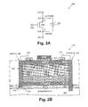
- FIG. 2A shows an exemplary circuit, including a silicon device and a group III-V transistor.
- exemplary circuit 200 comprises silicon Schottky diode 226 coupled in parallel with the source and drain of GaN HEMT 228.
- the anode of silicon Schottky diode 226 is connected to the source of GaN HEMT 228 at node 230, while the cathode of silicon Schottky diode 226 is connected to the drain of GaN HEMT 228 at node 232.
- Schottky diode 226 and GaN HEMT 228 can comprise discrete electrical components formed on different substrates of different dies.
- silicon Schottky diode 226 and GaN HEMT 228 can be monolithicaly integrated, for example, as shown and described in relation to Figure 2B .
- Figure 2B shows an exemplary monolithically integrated structure, in accordance with one embodiment of the present invention, corresponding to the circuit in Figure 2A .
- GaN HEMT structure 250 includes a group III-V transistor formed over substrate N+ 202.
- Various features of GaN HEMT structure 250 in Figure 2B have been discussed in relation to Figure 1 and are not repeated in relation to Figure 2B .
- elements in Figure 2B can correspond to elements having similar reference numerals in Figure 1 .
- AIGaN layer 214, GaN layer 212, and transition layers 210 and 208 can correspond to AIGaN layer 114, GaN layer 112, and transition layers 110 and 108 in Figure 1 and so on.
- GaN HEMT structure 250 is used as an example, the invention's concepts apply to GaN FETs, as wells as HEMTs and FETs made by use of different III-nitride or group III-V transistor structures.
- Source 216 of GaN HEMT structure 250 is connected to Epi N- layer 204 (for example a lightly doped region in Si) through interconnect metal connection 236 and via 238, referred to as an "anode via," in Figure 2B .
- Metal contact 240, at the bottom of anode via 238, comprises Schottky metal, for example, platinum, aluminum or other appropriate metals.
- a Schottky diode is produced in region 300 of Epi N- layer 204, which is circled in Figure 2B and shown in more detail as expanded structure 300 in Figure 3 .
- Drain 218 of GaN HEMT structure 250 is connected through interconnect metal connection 242 and via 244, referred to as a "cathode via," to substrate N+ 202, for example to an N+ silicon layer 202.
- the anode of silicon Schottky diode 226 in Figure 2A can correspond to metal contact 240
- the cathode of silicon Schottky diode 226 in Figure 2A can correspond to substrate N+ 202 connected to drain 218 through cathode via 244.
- anode via 238 extends along the group III-V transistor to contact the anode of the silicon diode and cathode via 244 and cathode via 244 extends along the group III-V transistor to contact the cathode of the silicon diode.
- Anode and cathode vias 238 and 244 generally do not have the same depth.
- metal contact 240 contact Epi N- layer 204 instead of substrate N+ 202, since the interface of metal contact 240 and substrate N+ 202 would have too high of a reverse bias leakage current and would also have reduced break down voltage.
- metal contact 240 can interface with Epi N- layer 204 to produce good Schottky contact and to support a higher breakdown voltage.
- Epi N- layer 204 can be, for example, about 0.5 to 10 microns thick. By making Epi N- layer 204 thicker, the breakdown voltage of the device can be increased.
- GaN HEMT structure 250 in Figure 2B can be an enhancement mode or depletion mode FET.
- Figure 3 shows an expanded view of region 300 showing the Schottky diode structure in more detail.
- substrate N+ 302, Epi N- layer 304, buffer 306, anode via 338, and metal contact 340 correspond respectively to substrate N+ 202, Epi N- layer 204, buffer layer 206, anode via 238, and metal contact 240 in Figure 2 .
- P+ regions for example, angled P+ implants can be used near corners 346 and 348 where metal contact 340 would be deposited.
- P+ angled implanting is performed at corners 346 and 348 of the trench.
- Typical P+ dopants such as Boron can be used.
- the center region of the anode can be blocked or masked so that P+ dopants can only diffuse into the corners of the region where metal contact 340 would interface with Epi N- layer 304.
- the combined device is a Schottky diode with PN junctions at corners 346 and 348. There is still a Schottky action in the center of metal contact 340 situated between the P+ regions.
- P+ regions at corners 346 and 348 increase breakdown voltage capability for two reasons.
- the PN junctions i.e. at corners 346 and 348) help spread-out the electric field to reduce electric field crowding at corners 346 and 348.
- the Schottky diode is reverse biased, there would be extended depletion regions near corners 346 and 348 at the P+ regions, which pinch off the Schottky diode and reduce the reverse leakage current so that higher voltages can be used due to a lower leakage current and higher breakdown voltage of this merged Schottky diode and PN junction configuration.
- P+ regions at corners 346 and 348 can raise breakdown voltage of the Schottky diode to 100 volts or more.
- a silicon Schottky diode as opposed to a GaN Schottky diode presents advantages.
- the forward bias voltage of the silicon Schottky diode is much lower than the forward bias voltage of a GaN Schottky diode.
- metals such as gold or copper or nickel are needed for Schottky metal in metal contact 340, which are not generally compatible with silicon CMOS processing.
- the monolithic integrated device of the present invention can however be fabricated in a silicon CMOS fabrication facility resulting in significant cost savings.
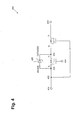
- Figure 4 shows an efficient high voltage switching circuit, in accordance with one embodiment of the present invention.
- circuit 400 employs GaN HEMTs or GaN FETs (or other III-nitride or group III-V transistors) 428 and 460 and silicon Schottky (or PN junction) diode 426.
- Silicon Schottky diode 426 can be integrated, and in one embodiment is integrated, with GaN device 428 and 460 shown in Figure 4 in a manner described above in relation to Figures 1 through 3 .
- various structures not shown in relation to Figure 4 can be similar to those described in relation to Figures 1 , 2B , and 3 .
- GaN device 428 which can be, for example, a GaN HEMT or GaN FET, can be an enhancement mode or depletion mode transistor, although GaN device 428 is preferably an enhancement mode transistor.
- GaN device 428 is a "low to medium" voltage GaN device, with breakdown voltage in the range of 10 to 50 volts.
- High voltage GaN device 460 typically has a breakdown voltage of over 100 volts (for example 100 to 1200 volts), and can be either an enhancement mode of depletion mode device, but it is preferably a depletion mode device.
- GaN device 428 is in parallel with silicon diode (silicon Schottky or PN junction diode) 426.
- the parallel arrangement of silicon diode 426 and GaN device 428 is in cascade with high voltage GaN device 460 and the gate of high voltage GaN device 460 is coupled to the source of GaN device 428 at node 462.
- Circuit 400 is shown having three terminals which can be connected to external circuits: terminal 464 conntected to node 462, terminal 434 connected to the gate of GaN HEMT 428, and terminal 466 connected to the drain of GaN HEMT 460. It is noted that the silicon/GaN semiconductor structure integration discussed in relation to Figures 1 through 3 can apply to the circuit of Figure 4 .
- circuit 400 in Figure 4 can be implemented as a monolithic (using a single die or a common or single substrate), cascaded, normally off high voltage switch.
- low voltage high efficiency silicon diode 426 (which can be either a Schottky or a PN junction diode) is in parallel with high performance low to medium voltage GaN device 428, which, in some embodiments, can correspond to GaN HEMT structure 250 in Figure 2B .
- the cascaded combination of silicon diode 426 and GaN device 428 with high voltage GaN device 460 results in high voltage handling capability, while using a high performance switch based on the parallel arrangement of two high performance devices silicon diode 426 and GaN device 428.
- circuit 400 is implemented as a monolithically integrated circuit, it incorporates various advantages discussed in relation to Figures 1 through 3 , and it overcomes the disadvantages of two separate dies discussed above.
- the monolithic structure corresponding to circuit 400 is much easier to package, and eliminates the parasitic inductance between the source of high voltage GaN device 460, and drain of low voltage GaN device 428.
- Figure 5A shows monolithically integrated structure 580, corresponding to an implementation of the circuit in Figure 4 , in accordance with one embodiment of the present invention. More particularly, Figure 5A shows integrated structure 580 corresponding to a further integration of circuit 400 of Figure 4 at a layout or floor plan level (which can be employed in addition to the structural integration shown and described in relation to Figures 1 through 3 ).
- Integrated structure 580 includes GaN devices 528 and 560 corresponding respectively to GaN devices 428 and 460 in Figure 4 .
- GaN device 528 includes source 516 and gate 520 and GaN device 560 includes drain 564 and gate 566.
- Integrated structure 580 further includes shared source/drain 562, where the source of GaN device 560 is shared on a layout level with the drain of GaN device 528, resulting in an enhanced level of integration.
- FIG 5A a portion of the interdigitated source, gate, and drain fingers of the laid out GaN device 528 and GaN device 560 is shown.
- the interdigitated configuration of Figure 5A can be repeated many times to arrive at the desired transistor size, but only one instance of the interdigitated configuration is shown in Figure 5A .
- the drain of GaN 528 and source of GaN 560 are shared in region 562. This technique not only reduces the area consumed on the die, but also eliminates inductive and resistive parasitics that would otherwise exist in connecting the drain of GaN 528 to the source of GaN 560.
- Figure 5B shows monolithically integrated structure 590, corresponding to an implementation of the circuit in Figure 4 , in accordance with one embodiment of the present invention.
- Figure 5B a portion of the interdigitated source, gate, and drain fingers of the laid out GaN device 528 and GaN device 560 is shown.
- the interdigitated configuration of Figure 5B is repeated many times to arrive at the desired transistor size, but only one instance of the interdigitated configuration is shown in Figure 5B .
- drain 518 of GaN device 528 and source 566 of GaN device 560 are connected to each other by interconnect metal segments, such as interconnect metal segment 568 and contacts 570 and 572.
- Figure 5B Typically a large number of metal segments are used, but only one example of such metal segments is shown in Figure 5B . According to Figure 5B , the various disadvantages associated with two separate dies are eliminated due to the silicon/GaN integration scheme discussed in relation to Figures 1 through 3 , and only a small amount of inductive and resistive parasitics are present due to the connection between drain 518 of GaN 528 and source 566 of GaN 560.
- the present invention achieves an efficient high voltage switching circuit.
- a silicon diode is coupled in parallel with the source and drain of a GaN HEMT, where the parallel arrangement of the silicon diode and the GaN HEMT is in cascade with a high voltage GaN HEMT.
- the resulting switching circuit can provide high voltage handling capability, performance capability, and input gate characteristics.
- fabrication cost, packaging cost, and area consumed on a PC board can be reduced.
- parasitic inductance, capacitance, and resistance can be reduced by removing interconnections at the packaging level and the PC board level.
- the invention furhter reduces the area consumed on the die and eliminates inductive and resistive parasitics resulting in, for example, reduced noise and ringing, increased stability, and enhanced performance of the switching circuit.
Landscapes
- Junction Field-Effect Transistors (AREA)
- Electrodes Of Semiconductors (AREA)
- Internal Circuitry In Semiconductor Integrated Circuit Devices (AREA)
- Electronic Switches (AREA)
Applications Claiming Priority (2)
| Application Number | Priority Date | Filing Date | Title |
|---|---|---|---|
| US33919010P | 2010-03-01 | 2010-03-01 | |
| US13/020,243 US9219058B2 (en) | 2010-03-01 | 2011-02-03 | Efficient high voltage switching circuits and monolithic integration of same |
Publications (3)
| Publication Number | Publication Date |
|---|---|
| EP2363885A2 true EP2363885A2 (fr) | 2011-09-07 |
| EP2363885A3 EP2363885A3 (fr) | 2014-01-22 |
| EP2363885B1 EP2363885B1 (fr) | 2020-05-27 |
Family
ID=44504829
Family Applications (1)
| Application Number | Title | Priority Date | Filing Date |
|---|---|---|---|
| EP11001113.7A Not-in-force EP2363885B1 (fr) | 2010-03-01 | 2011-02-11 | Circuits de commutation efficace haute tension et leur intégration monolithique |
Country Status (3)
| Country | Link |
|---|---|
| US (1) | US9219058B2 (fr) |
| EP (1) | EP2363885B1 (fr) |
| JP (1) | JP4897929B2 (fr) |
Families Citing this family (25)
| Publication number | Priority date | Publication date | Assignee | Title |
|---|---|---|---|---|
| US9219058B2 (en) | 2010-03-01 | 2015-12-22 | Infineon Technologies Americas Corp. | Efficient high voltage switching circuits and monolithic integration of same |
| US8981380B2 (en) * | 2010-03-01 | 2015-03-17 | International Rectifier Corporation | Monolithic integration of silicon and group III-V devices |
| JP5789967B2 (ja) * | 2010-12-03 | 2015-10-07 | 富士通株式会社 | 半導体装置及びその製造方法、電源装置 |
| US8847408B2 (en) * | 2011-03-02 | 2014-09-30 | International Rectifier Corporation | III-nitride transistor stacked with FET in a package |
| US9859882B2 (en) | 2011-03-21 | 2018-01-02 | Infineon Technologies Americas Corp. | High voltage composite semiconductor device with protection for a low voltage device |
| US9236376B2 (en) | 2011-03-21 | 2016-01-12 | Infineon Technologies Americas Corp. | Power semiconductor device with oscillation prevention |
| US9362905B2 (en) | 2011-03-21 | 2016-06-07 | Infineon Technologies Americas Corp. | Composite semiconductor device with turn-on prevention control |
| US9281388B2 (en) | 2011-07-15 | 2016-03-08 | Infineon Technologies Americas Corp. | Composite semiconductor device with a SOI substrate having an integrated diode |
| US20130087803A1 (en) * | 2011-10-06 | 2013-04-11 | Epowersoft, Inc. | Monolithically integrated hemt and schottky diode |
| JP5678866B2 (ja) | 2011-10-31 | 2015-03-04 | 株式会社デンソー | 半導体装置およびその製造方法 |
| US8587033B1 (en) | 2012-06-04 | 2013-11-19 | Infineon Technologies Austria Ag | Monolithically integrated HEMT and current protection device |
| TWI567930B (zh) * | 2012-11-19 | 2017-01-21 | 台達電子工業股份有限公司 | 半導體裝置 |
| US9202811B2 (en) * | 2012-12-18 | 2015-12-01 | Infineon Technologies Americas Corp. | Cascode circuit integration of group III-N and group IV devices |
| US9269789B2 (en) | 2013-03-15 | 2016-02-23 | Semiconductor Components Industries, Llc | Method of forming a high electron mobility semiconductor device and structure therefor |
| US9842923B2 (en) | 2013-03-15 | 2017-12-12 | Semiconductor Components Industries, Llc | Ohmic contact structure for semiconductor device and method |
| US9184243B2 (en) * | 2013-07-12 | 2015-11-10 | Infineon Technologies Americas Corp. | Monolithic composite III-nitride transistor with high voltage group IV enable switch |
| US9257424B2 (en) | 2013-11-08 | 2016-02-09 | Infineon Technologies Austria Ag | Semiconductor device |
| US20160005845A1 (en) * | 2014-07-02 | 2016-01-07 | International Rectifier Corporation | Group III-V Transistor Utilizing a Substrate Having a Dielectrically-Filled Region |
| US10587194B2 (en) | 2014-08-20 | 2020-03-10 | Navitas Semiconductor, Inc. | Power transistor with distributed gate |
| US9741711B2 (en) * | 2014-10-28 | 2017-08-22 | Semiconductor Components Industries, Llc | Cascode semiconductor device structure and method therefor |
| US9356017B1 (en) | 2015-02-05 | 2016-05-31 | Infineon Technologies Austria Ag | Switch circuit and semiconductor device |
| US9941265B2 (en) * | 2016-07-01 | 2018-04-10 | Nexperia B.V. | Circuitry with voltage limiting and capactive enhancement |
| US10991722B2 (en) * | 2019-03-15 | 2021-04-27 | International Business Machines Corporation | Ultra low parasitic inductance integrated cascode GaN devices |
| CN111312712A (zh) * | 2020-02-25 | 2020-06-19 | 英诺赛科(珠海)科技有限公司 | 半导体器件及其制造方法 |
| US11784189B2 (en) | 2021-08-20 | 2023-10-10 | Globalfoundries U.S. Inc. | Monolithic integration of diverse device types with shared electrical isolation |
Family Cites Families (69)
| Publication number | Priority date | Publication date | Assignee | Title |
|---|---|---|---|---|
| US799288A (en) * | 1905-04-12 | 1905-09-12 | John W Yochem | Dashboard-holder. |
| US5021840A (en) * | 1987-08-18 | 1991-06-04 | Texas Instruments Incorporated | Schottky or PN diode with composite sidewall |
| WO2001006546A2 (fr) * | 1999-07-16 | 2001-01-25 | Massachusetts Institute Of Technology | Liaison silicium iii-v d'un semiconducteur destinee a une integration monolithique optoelectronique |
| US6433396B1 (en) * | 1999-10-05 | 2002-08-13 | International Rectifier Corporation | Trench MOSFET with integrated schottky device and process for its manufacture |
| JP5130641B2 (ja) * | 2006-03-31 | 2013-01-30 | サンケン電気株式会社 | 複合半導体装置 |
| WO2004040761A1 (fr) * | 2002-10-29 | 2004-05-13 | Koninklijke Philips Electronics N.V. | Commutateur a deux transistors nmos bidirectionnel |
| US7550781B2 (en) * | 2004-02-12 | 2009-06-23 | International Rectifier Corporation | Integrated III-nitride power devices |
| JP2006310769A (ja) * | 2005-02-02 | 2006-11-09 | Internatl Rectifier Corp | Iii族窒化物一体化ショットキおよび電力素子 |
| US8866190B2 (en) * | 2005-06-14 | 2014-10-21 | International Rectifler Corporation | Methods of combining silicon and III-nitride material on a single wafer |
| US8168000B2 (en) * | 2005-06-15 | 2012-05-01 | International Rectifier Corporation | III-nitride semiconductor device fabrication |
| US8183595B2 (en) * | 2005-07-29 | 2012-05-22 | International Rectifier Corporation | Normally off III-nitride semiconductor device having a programmable gate |
| US8482035B2 (en) * | 2005-07-29 | 2013-07-09 | International Rectifier Corporation | Enhancement mode III-nitride transistors with single gate Dielectric structure |
| US8614129B2 (en) * | 2005-09-30 | 2013-12-24 | International Rectifier Corporation | Method for fabricating a semiconductor device |
| JP4772542B2 (ja) | 2006-03-15 | 2011-09-14 | 株式会社東芝 | 電力変換装置 |
| US7875958B2 (en) * | 2006-09-27 | 2011-01-25 | Taiwan Semiconductor Manufacturing Company, Ltd. | Quantum tunneling devices and circuits with lattice-mismatched semiconductor structures |
| US7964895B2 (en) * | 2006-10-05 | 2011-06-21 | International Rectifier Corporation | III-nitride heterojunction semiconductor device and method of fabrication |
| US7902809B2 (en) * | 2006-11-28 | 2011-03-08 | International Rectifier Corporation | DC/DC converter including a depletion mode power switch |
| US8674670B2 (en) * | 2006-11-28 | 2014-03-18 | International Rectifier Corporation | DC/DC converter with depletion-mode III-nitride switches |
| US7863877B2 (en) * | 2006-12-11 | 2011-01-04 | International Rectifier Corporation | Monolithically integrated III-nitride power converter |
| WO2008086001A2 (fr) * | 2007-01-10 | 2008-07-17 | International Rectifier Corporation | Mise en forme de zone active pour dispositif au nitrure iii et procédé de fabrication |
| JP5358882B2 (ja) * | 2007-02-09 | 2013-12-04 | サンケン電気株式会社 | 整流素子を含む複合半導体装置 |
| US7501670B2 (en) | 2007-03-20 | 2009-03-10 | Velox Semiconductor Corporation | Cascode circuit employing a depletion-mode, GaN-based FET |
| JP4691060B2 (ja) * | 2007-03-23 | 2011-06-01 | 古河電気工業株式会社 | GaN系半導体素子 |
| JP5319084B2 (ja) | 2007-06-19 | 2013-10-16 | ルネサスエレクトロニクス株式会社 | 半導体装置 |
| US8093597B2 (en) * | 2007-06-25 | 2012-01-10 | International Rectifier Corporation | In situ dopant implantation and growth of a III-nitride semiconductor body |
| US8395132B2 (en) * | 2007-06-25 | 2013-03-12 | International Rectifier Corporation | Ion implanting while growing a III-nitride layer |
| US8174051B2 (en) * | 2007-06-26 | 2012-05-08 | International Rectifier Corporation | III-nitride power device |
| CN101682720A (zh) * | 2007-06-27 | 2010-03-24 | 国际整流器公司 | 在降压变换器中耗尽型器件的栅极驱动方案 |
| US20090050939A1 (en) * | 2007-07-17 | 2009-02-26 | Briere Michael A | Iii-nitride device |
| EP2887402B1 (fr) * | 2007-09-12 | 2019-06-12 | Transphorm Inc. | Commutateurs bidirectionnels en III nitrure |
| US8791503B2 (en) * | 2007-09-18 | 2014-07-29 | International Rectifier Corporation | III-nitride semiconductor device with reduced electric field between gate and drain and process for its manufacture |
| US8680579B2 (en) * | 2007-09-20 | 2014-03-25 | International Rectifier Corporation | Individually controlled multiple III-nitride half bridges |
| WO2009038809A1 (fr) * | 2007-09-20 | 2009-03-26 | International Rectifier Corporation | Dispositif semi-conducteur au nitrure du groupe iii à mode d'enrichissement à champ électrique réduit entre la grille et le drain |
| US8159003B2 (en) * | 2007-11-26 | 2012-04-17 | International Rectifier Corporation | III-nitride wafer and devices formed in a III-nitride wafer |
| US7999288B2 (en) * | 2007-11-26 | 2011-08-16 | International Rectifier Corporation | High voltage durability III-nitride semiconductor device |
| JP2009164158A (ja) * | 2007-12-28 | 2009-07-23 | Panasonic Corp | 半導体装置及びその製造方法 |
| US8063616B2 (en) * | 2008-01-11 | 2011-11-22 | International Rectifier Corporation | Integrated III-nitride power converter circuit |
| JP2009182107A (ja) * | 2008-01-30 | 2009-08-13 | Furukawa Electric Co Ltd:The | 半導体装置 |
| JP2009246045A (ja) | 2008-03-28 | 2009-10-22 | Furukawa Electric Co Ltd:The | 電界効果トランジスタ及びその製造方法 |
| US8076699B2 (en) * | 2008-04-02 | 2011-12-13 | The Hong Kong Univ. Of Science And Technology | Integrated HEMT and lateral field-effect rectifier combinations, methods, and systems |
| US9159679B2 (en) * | 2008-09-15 | 2015-10-13 | International Rectifier Corporation | Semiconductor package with integrated passives and method for fabricating same |
| EP2394299B8 (fr) * | 2009-02-03 | 2017-01-25 | NXP USA, Inc. | Structure semi-conductrice et procédé de fabrication d'une telle structure |
| US7915645B2 (en) * | 2009-05-28 | 2011-03-29 | International Rectifier Corporation | Monolithic vertically integrated composite group III-V and group IV semiconductor device and method for fabricating same |
| US8138529B2 (en) * | 2009-11-02 | 2012-03-20 | Transphorm Inc. | Package configurations for low EMI circuits |
| US8530938B2 (en) * | 2009-12-10 | 2013-09-10 | International Rectifier Corporation | Monolithic integrated composite group III-V and group IV semiconductor device and method for fabricating same |
| US9378965B2 (en) * | 2009-12-10 | 2016-06-28 | Infineon Technologies Americas Corp. | Highly conductive source/drain contacts in III-nitride transistors |
| US8399912B2 (en) * | 2010-02-16 | 2013-03-19 | International Rectifier Corporation | III-nitride power device with solderable front metal |
| US8981380B2 (en) * | 2010-03-01 | 2015-03-17 | International Rectifier Corporation | Monolithic integration of silicon and group III-V devices |
| US9219058B2 (en) | 2010-03-01 | 2015-12-22 | Infineon Technologies Americas Corp. | Efficient high voltage switching circuits and monolithic integration of same |
| US9105703B2 (en) * | 2010-03-22 | 2015-08-11 | International Rectifier Corporation | Programmable III-nitride transistor with aluminum-doped gate |
| US20110260210A1 (en) * | 2010-04-23 | 2011-10-27 | Applied Materials, Inc. | Gan-based leds on silicon substrates with monolithically integrated zener diodes |
| JP5707903B2 (ja) * | 2010-12-02 | 2015-04-30 | 富士通株式会社 | 化合物半導体装置及びその製造方法 |
| JP6018360B2 (ja) * | 2010-12-02 | 2016-11-02 | 富士通株式会社 | 化合物半導体装置及びその製造方法 |
| JP5741042B2 (ja) * | 2011-02-14 | 2015-07-01 | 富士通株式会社 | 化合物半導体装置及びその製造方法 |
| US8659030B2 (en) * | 2011-02-28 | 2014-02-25 | International Rectifier Corporation | III-nitride heterojunction devices having a multilayer spacer |
| US8957454B2 (en) * | 2011-03-03 | 2015-02-17 | International Rectifier Corporation | III-Nitride semiconductor structures with strain absorbing interlayer transition modules |
| US9076853B2 (en) * | 2011-03-18 | 2015-07-07 | International Rectifie Corporation | High voltage rectifier and switching circuits |
| US20120241820A1 (en) * | 2011-03-21 | 2012-09-27 | International Rectifier Corporation | III-Nitride Transistor with Passive Oscillation Prevention |
| US8987833B2 (en) * | 2011-04-11 | 2015-03-24 | International Rectifier Corporation | Stacked composite device including a group III-V transistor and a group IV lateral transistor |
| US9343440B2 (en) * | 2011-04-11 | 2016-05-17 | Infineon Technologies Americas Corp. | Stacked composite device including a group III-V transistor and a group IV vertical transistor |
| US20120256190A1 (en) * | 2011-04-11 | 2012-10-11 | International Rectifier Corporation | Stacked Composite Device Including a Group III-V Transistor and a Group IV Diode |
| US20120274366A1 (en) * | 2011-04-28 | 2012-11-01 | International Rectifier Corporation | Integrated Power Stage |
| US8988133B2 (en) * | 2011-07-11 | 2015-03-24 | International Rectifier Corporation | Nested composite switch |
| US20130015501A1 (en) * | 2011-07-11 | 2013-01-17 | International Rectifier Corporation | Nested Composite Diode |
| US9281388B2 (en) * | 2011-07-15 | 2016-03-08 | Infineon Technologies Americas Corp. | Composite semiconductor device with a SOI substrate having an integrated diode |
| US9087812B2 (en) * | 2011-07-15 | 2015-07-21 | International Rectifier Corporation | Composite semiconductor device with integrated diode |
| JP5891650B2 (ja) * | 2011-08-18 | 2016-03-23 | 富士通株式会社 | 化合物半導体装置及びその製造方法 |
| US8796738B2 (en) * | 2011-09-21 | 2014-08-05 | International Rectifier Corporation | Group III-V device structure having a selectively reduced impurity concentration |
| US9147701B2 (en) * | 2011-09-22 | 2015-09-29 | Raytheon Company | Monolithic InGaN solar cell power generation with integrated efficient switching DC-DC voltage convertor |
-
2011
- 2011-02-03 US US13/020,243 patent/US9219058B2/en not_active Expired - Fee Related
- 2011-02-11 EP EP11001113.7A patent/EP2363885B1/fr not_active Not-in-force
- 2011-02-21 JP JP2011034833A patent/JP4897929B2/ja not_active Expired - Fee Related
Non-Patent Citations (1)
| Title |
|---|
| None |
Also Published As
| Publication number | Publication date |
|---|---|
| EP2363885A3 (fr) | 2014-01-22 |
| EP2363885B1 (fr) | 2020-05-27 |
| US9219058B2 (en) | 2015-12-22 |
| JP4897929B2 (ja) | 2012-03-14 |
| JP2011205622A (ja) | 2011-10-13 |
| US20110210338A1 (en) | 2011-09-01 |
Similar Documents
| Publication | Publication Date | Title |
|---|---|---|
| US9219058B2 (en) | Efficient high voltage switching circuits and monolithic integration of same | |
| US8981380B2 (en) | Monolithic integration of silicon and group III-V devices | |
| US10204998B2 (en) | Heterostructure device | |
| US9171937B2 (en) | Monolithically integrated vertical JFET and Schottky diode | |
| US9184243B2 (en) | Monolithic composite III-nitride transistor with high voltage group IV enable switch | |
| US7439556B2 (en) | Substrate driven field-effect transistor | |
| US20130087803A1 (en) | Monolithically integrated hemt and schottky diode | |
| US9300223B2 (en) | Rectifying circuit and semiconductor device | |
| US8368119B1 (en) | Integrated structure with transistors and schottky diodes and process for fabricating the same | |
| US10505032B2 (en) | Semiconductor device with III-nitride channel region and silicon carbide drift region | |
| US20140319532A1 (en) | Heterojunction Semiconductor Device and Manufacturing Method | |
| EP4629776A2 (fr) | Dispositif semi-conducteur de commutation bidirectionnel à semi-conducteur à base de nitrure et son procédé de fabrication | |
| CN111213241B (zh) | 半导体器件、半导体设备及其制造方法 | |
| US20130062614A1 (en) | Group iii-v enhancement mode transistor with thyristor gate | |
| US8552562B2 (en) | Profiled contact for semiconductor device | |
| US12446300B2 (en) | Semiconductor devices having on-chip gate resistors | |
| US20260123030A1 (en) | P-type nitride-based transistor | |
| CN115997287B (zh) | 氮化物基半导体ic芯片及其制造方法 | |
| US20250169156A1 (en) | High electron mobility transistor with integrated diode | |
| KR20250143516A (ko) | 반도체 장치 및 이를 포함하는 전력 시스템 |
Legal Events
| Date | Code | Title | Description |
|---|---|---|---|
| PUAI | Public reference made under article 153(3) epc to a published international application that has entered the european phase |
Free format text: ORIGINAL CODE: 0009012 |
|
| AK | Designated contracting states |
Kind code of ref document: A2 Designated state(s): AL AT BE BG CH CY CZ DE DK EE ES FI FR GB GR HR HU IE IS IT LI LT LU LV MC MK MT NL NO PL PT RO RS SE SI SK SM TR |
|
| AX | Request for extension of the european patent |
Extension state: BA ME |
|
| PUAL | Search report despatched |
Free format text: ORIGINAL CODE: 0009013 |
|
| AK | Designated contracting states |
Kind code of ref document: A3 Designated state(s): AL AT BE BG CH CY CZ DE DK EE ES FI FR GB GR HR HU IE IS IT LI LT LU LV MC MK MT NL NO PL PT RO RS SE SI SK SM TR |
|
| AX | Request for extension of the european patent |
Extension state: BA ME |
|
| RIC1 | Information provided on ipc code assigned before grant |
Ipc: H01L 21/8252 20060101ALI20131219BHEP Ipc: H03K 17/567 20060101ALI20131219BHEP Ipc: H01L 27/088 20060101ALN20131219BHEP Ipc: H01L 27/06 20060101AFI20131219BHEP Ipc: H01L 21/8258 20060101ALI20131219BHEP |
|
| 17P | Request for examination filed |
Effective date: 20140722 |
|
| RBV | Designated contracting states (corrected) |
Designated state(s): AL AT BE BG CH CY CZ DE DK EE ES FI FR GB GR HR HU IE IS IT LI LT LU LV MC MK MT NL NO PL PT RO RS SE SI SK SM TR |
|
| 17Q | First examination report despatched |
Effective date: 20160727 |
|
| STAA | Information on the status of an ep patent application or granted ep patent |
Free format text: STATUS: EXAMINATION IS IN PROGRESS |
|
| RAP1 | Party data changed (applicant data changed or rights of an application transferred) |
Owner name: INFINEON TECHNOLOGIES AMERICAS CORP. |
|
| RIC1 | Information provided on ipc code assigned before grant |
Ipc: H01L 29/778 20060101ALI20191031BHEP Ipc: H01L 27/088 20060101ALN20191031BHEP Ipc: H01L 29/20 20060101ALN20191031BHEP Ipc: H01L 21/8258 20060101ALI20191031BHEP Ipc: H03K 17/567 20060101ALI20191031BHEP Ipc: H01L 27/06 20060101AFI20191031BHEP |
|
| GRAP | Despatch of communication of intention to grant a patent |
Free format text: ORIGINAL CODE: EPIDOSNIGR1 |
|
| STAA | Information on the status of an ep patent application or granted ep patent |
Free format text: STATUS: GRANT OF PATENT IS INTENDED |
|
| RIC1 | Information provided on ipc code assigned before grant |
Ipc: H01L 27/06 20060101AFI20191202BHEP Ipc: H01L 27/088 20060101ALN20191202BHEP Ipc: H01L 29/778 20060101ALI20191202BHEP Ipc: H01L 21/8258 20060101ALI20191202BHEP Ipc: H01L 29/20 20060101ALN20191202BHEP Ipc: H03K 17/567 20060101ALI20191202BHEP |
|
| INTG | Intention to grant announced |
Effective date: 20191216 |
|
| GRAS | Grant fee paid |
Free format text: ORIGINAL CODE: EPIDOSNIGR3 |
|
| GRAA | (expected) grant |
Free format text: ORIGINAL CODE: 0009210 |
|
| STAA | Information on the status of an ep patent application or granted ep patent |
Free format text: STATUS: THE PATENT HAS BEEN GRANTED |
|
| AK | Designated contracting states |
Kind code of ref document: B1 Designated state(s): AL AT BE BG CH CY CZ DE DK EE ES FI FR GB GR HR HU IE IS IT LI LT LU LV MC MK MT NL NO PL PT RO RS SE SI SK SM TR |
|
| REG | Reference to a national code |
Ref country code: GB Ref legal event code: FG4D |
|
| REG | Reference to a national code |
Ref country code: CH Ref legal event code: EP |
|
| REG | Reference to a national code |
Ref country code: DE Ref legal event code: R096 Ref document number: 602011066998 Country of ref document: DE |
|
| REG | Reference to a national code |
Ref country code: AT Ref legal event code: REF Ref document number: 1275460 Country of ref document: AT Kind code of ref document: T Effective date: 20200615 |
|
| REG | Reference to a national code |
Ref country code: LT Ref legal event code: MG4D |
|
| PG25 | Lapsed in a contracting state [announced via postgrant information from national office to epo] |
Ref country code: PT Free format text: LAPSE BECAUSE OF FAILURE TO SUBMIT A TRANSLATION OF THE DESCRIPTION OR TO PAY THE FEE WITHIN THE PRESCRIBED TIME-LIMIT Effective date: 20200928 Ref country code: NO Free format text: LAPSE BECAUSE OF FAILURE TO SUBMIT A TRANSLATION OF THE DESCRIPTION OR TO PAY THE FEE WITHIN THE PRESCRIBED TIME-LIMIT Effective date: 20200827 Ref country code: IS Free format text: LAPSE BECAUSE OF FAILURE TO SUBMIT A TRANSLATION OF THE DESCRIPTION OR TO PAY THE FEE WITHIN THE PRESCRIBED TIME-LIMIT Effective date: 20200927 Ref country code: GR Free format text: LAPSE BECAUSE OF FAILURE TO SUBMIT A TRANSLATION OF THE DESCRIPTION OR TO PAY THE FEE WITHIN THE PRESCRIBED TIME-LIMIT Effective date: 20200828 Ref country code: FI Free format text: LAPSE BECAUSE OF FAILURE TO SUBMIT A TRANSLATION OF THE DESCRIPTION OR TO PAY THE FEE WITHIN THE PRESCRIBED TIME-LIMIT Effective date: 20200527 Ref country code: LT Free format text: LAPSE BECAUSE OF FAILURE TO SUBMIT A TRANSLATION OF THE DESCRIPTION OR TO PAY THE FEE WITHIN THE PRESCRIBED TIME-LIMIT Effective date: 20200527 Ref country code: SE Free format text: LAPSE BECAUSE OF FAILURE TO SUBMIT A TRANSLATION OF THE DESCRIPTION OR TO PAY THE FEE WITHIN THE PRESCRIBED TIME-LIMIT Effective date: 20200527 |
|
| REG | Reference to a national code |
Ref country code: NL Ref legal event code: MP Effective date: 20200527 |
|
| PG25 | Lapsed in a contracting state [announced via postgrant information from national office to epo] |
Ref country code: BG Free format text: LAPSE BECAUSE OF FAILURE TO SUBMIT A TRANSLATION OF THE DESCRIPTION OR TO PAY THE FEE WITHIN THE PRESCRIBED TIME-LIMIT Effective date: 20200827 Ref country code: RS Free format text: LAPSE BECAUSE OF FAILURE TO SUBMIT A TRANSLATION OF THE DESCRIPTION OR TO PAY THE FEE WITHIN THE PRESCRIBED TIME-LIMIT Effective date: 20200527 Ref country code: HR Free format text: LAPSE BECAUSE OF FAILURE TO SUBMIT A TRANSLATION OF THE DESCRIPTION OR TO PAY THE FEE WITHIN THE PRESCRIBED TIME-LIMIT Effective date: 20200527 Ref country code: LV Free format text: LAPSE BECAUSE OF FAILURE TO SUBMIT A TRANSLATION OF THE DESCRIPTION OR TO PAY THE FEE WITHIN THE PRESCRIBED TIME-LIMIT Effective date: 20200527 |
|
| REG | Reference to a national code |
Ref country code: AT Ref legal event code: MK05 Ref document number: 1275460 Country of ref document: AT Kind code of ref document: T Effective date: 20200527 |
|
| PG25 | Lapsed in a contracting state [announced via postgrant information from national office to epo] |
Ref country code: AL Free format text: LAPSE BECAUSE OF FAILURE TO SUBMIT A TRANSLATION OF THE DESCRIPTION OR TO PAY THE FEE WITHIN THE PRESCRIBED TIME-LIMIT Effective date: 20200527 Ref country code: NL Free format text: LAPSE BECAUSE OF FAILURE TO SUBMIT A TRANSLATION OF THE DESCRIPTION OR TO PAY THE FEE WITHIN THE PRESCRIBED TIME-LIMIT Effective date: 20200527 |
|
| PG25 | Lapsed in a contracting state [announced via postgrant information from national office to epo] |
Ref country code: AT Free format text: LAPSE BECAUSE OF FAILURE TO SUBMIT A TRANSLATION OF THE DESCRIPTION OR TO PAY THE FEE WITHIN THE PRESCRIBED TIME-LIMIT Effective date: 20200527 Ref country code: SM Free format text: LAPSE BECAUSE OF FAILURE TO SUBMIT A TRANSLATION OF THE DESCRIPTION OR TO PAY THE FEE WITHIN THE PRESCRIBED TIME-LIMIT Effective date: 20200527 Ref country code: IT Free format text: LAPSE BECAUSE OF FAILURE TO SUBMIT A TRANSLATION OF THE DESCRIPTION OR TO PAY THE FEE WITHIN THE PRESCRIBED TIME-LIMIT Effective date: 20200527 Ref country code: EE Free format text: LAPSE BECAUSE OF FAILURE TO SUBMIT A TRANSLATION OF THE DESCRIPTION OR TO PAY THE FEE WITHIN THE PRESCRIBED TIME-LIMIT Effective date: 20200527 Ref country code: ES Free format text: LAPSE BECAUSE OF FAILURE TO SUBMIT A TRANSLATION OF THE DESCRIPTION OR TO PAY THE FEE WITHIN THE PRESCRIBED TIME-LIMIT Effective date: 20200527 Ref country code: DK Free format text: LAPSE BECAUSE OF FAILURE TO SUBMIT A TRANSLATION OF THE DESCRIPTION OR TO PAY THE FEE WITHIN THE PRESCRIBED TIME-LIMIT Effective date: 20200527 Ref country code: CZ Free format text: LAPSE BECAUSE OF FAILURE TO SUBMIT A TRANSLATION OF THE DESCRIPTION OR TO PAY THE FEE WITHIN THE PRESCRIBED TIME-LIMIT Effective date: 20200527 Ref country code: RO Free format text: LAPSE BECAUSE OF FAILURE TO SUBMIT A TRANSLATION OF THE DESCRIPTION OR TO PAY THE FEE WITHIN THE PRESCRIBED TIME-LIMIT Effective date: 20200527 |
|
| PG25 | Lapsed in a contracting state [announced via postgrant information from national office to epo] |
Ref country code: SK Free format text: LAPSE BECAUSE OF FAILURE TO SUBMIT A TRANSLATION OF THE DESCRIPTION OR TO PAY THE FEE WITHIN THE PRESCRIBED TIME-LIMIT Effective date: 20200527 Ref country code: PL Free format text: LAPSE BECAUSE OF FAILURE TO SUBMIT A TRANSLATION OF THE DESCRIPTION OR TO PAY THE FEE WITHIN THE PRESCRIBED TIME-LIMIT Effective date: 20200527 |
|
| REG | Reference to a national code |
Ref country code: DE Ref legal event code: R097 Ref document number: 602011066998 Country of ref document: DE |
|
| PLBE | No opposition filed within time limit |
Free format text: ORIGINAL CODE: 0009261 |
|
| STAA | Information on the status of an ep patent application or granted ep patent |
Free format text: STATUS: NO OPPOSITION FILED WITHIN TIME LIMIT |
|
| 26N | No opposition filed |
Effective date: 20210302 |
|
| PG25 | Lapsed in a contracting state [announced via postgrant information from national office to epo] |
Ref country code: SI Free format text: LAPSE BECAUSE OF FAILURE TO SUBMIT A TRANSLATION OF THE DESCRIPTION OR TO PAY THE FEE WITHIN THE PRESCRIBED TIME-LIMIT Effective date: 20200527 |
|
| PG25 | Lapsed in a contracting state [announced via postgrant information from national office to epo] |
Ref country code: MC Free format text: LAPSE BECAUSE OF FAILURE TO SUBMIT A TRANSLATION OF THE DESCRIPTION OR TO PAY THE FEE WITHIN THE PRESCRIBED TIME-LIMIT Effective date: 20200527 |
|
| GBPC | Gb: european patent ceased through non-payment of renewal fee |
Effective date: 20210211 |
|
| REG | Reference to a national code |
Ref country code: BE Ref legal event code: MM Effective date: 20210228 |
|
| PG25 | Lapsed in a contracting state [announced via postgrant information from national office to epo] |
Ref country code: CH Free format text: LAPSE BECAUSE OF NON-PAYMENT OF DUE FEES Effective date: 20210228 Ref country code: LU Free format text: LAPSE BECAUSE OF NON-PAYMENT OF DUE FEES Effective date: 20210211 Ref country code: LI Free format text: LAPSE BECAUSE OF NON-PAYMENT OF DUE FEES Effective date: 20210228 |
|
| PG25 | Lapsed in a contracting state [announced via postgrant information from national office to epo] |
Ref country code: FR Free format text: LAPSE BECAUSE OF NON-PAYMENT OF DUE FEES Effective date: 20210228 Ref country code: GB Free format text: LAPSE BECAUSE OF NON-PAYMENT OF DUE FEES Effective date: 20210211 Ref country code: IE Free format text: LAPSE BECAUSE OF NON-PAYMENT OF DUE FEES Effective date: 20210211 |
|
| PG25 | Lapsed in a contracting state [announced via postgrant information from national office to epo] |
Ref country code: BE Free format text: LAPSE BECAUSE OF NON-PAYMENT OF DUE FEES Effective date: 20210228 |
|
| PGFP | Annual fee paid to national office [announced via postgrant information from national office to epo] |
Ref country code: DE Payment date: 20220421 Year of fee payment: 12 |
|
| PG25 | Lapsed in a contracting state [announced via postgrant information from national office to epo] |
Ref country code: HU Free format text: LAPSE BECAUSE OF FAILURE TO SUBMIT A TRANSLATION OF THE DESCRIPTION OR TO PAY THE FEE WITHIN THE PRESCRIBED TIME-LIMIT; INVALID AB INITIO Effective date: 20110211 Ref country code: CY Free format text: LAPSE BECAUSE OF FAILURE TO SUBMIT A TRANSLATION OF THE DESCRIPTION OR TO PAY THE FEE WITHIN THE PRESCRIBED TIME-LIMIT Effective date: 20200527 |
|
| REG | Reference to a national code |
Ref country code: DE Ref legal event code: R119 Ref document number: 602011066998 Country of ref document: DE |
|
| PG25 | Lapsed in a contracting state [announced via postgrant information from national office to epo] |
Ref country code: DE Free format text: LAPSE BECAUSE OF NON-PAYMENT OF DUE FEES Effective date: 20230901 |
|
| PG25 | Lapsed in a contracting state [announced via postgrant information from national office to epo] |
Ref country code: MK Free format text: LAPSE BECAUSE OF FAILURE TO SUBMIT A TRANSLATION OF THE DESCRIPTION OR TO PAY THE FEE WITHIN THE PRESCRIBED TIME-LIMIT Effective date: 20200527 |
|
| PG25 | Lapsed in a contracting state [announced via postgrant information from national office to epo] |
Ref country code: TR Free format text: LAPSE BECAUSE OF FAILURE TO SUBMIT A TRANSLATION OF THE DESCRIPTION OR TO PAY THE FEE WITHIN THE PRESCRIBED TIME-LIMIT Effective date: 20200527 |
|
| PG25 | Lapsed in a contracting state [announced via postgrant information from national office to epo] |
Ref country code: MT Free format text: LAPSE BECAUSE OF FAILURE TO SUBMIT A TRANSLATION OF THE DESCRIPTION OR TO PAY THE FEE WITHIN THE PRESCRIBED TIME-LIMIT Effective date: 20200527 |