EP2364459B1 - Structure et procédé pour adapter la polarité d'une source de puissance à un système électrochromique - Google Patents
Structure et procédé pour adapter la polarité d'une source de puissance à un système électrochromique Download PDFInfo
- Publication number
- EP2364459B1 EP2364459B1 EP09752136.3A EP09752136A EP2364459B1 EP 2364459 B1 EP2364459 B1 EP 2364459B1 EP 09752136 A EP09752136 A EP 09752136A EP 2364459 B1 EP2364459 B1 EP 2364459B1
- Authority
- EP
- European Patent Office
- Prior art keywords
- polarity
- electrical
- power source
- terminal
- pole
- Prior art date
- Legal status (The legal status is an assumption and is not a legal conclusion. Google has not performed a legal analysis and makes no representation as to the accuracy of the status listed.)
- Not-in-force
Links
- 238000000034 method Methods 0.000 title claims description 16
- 230000003287 optical effect Effects 0.000 claims description 39
- 230000008859 change Effects 0.000 claims description 6
- 238000005259 measurement Methods 0.000 claims description 6
- 230000001276 controlling effect Effects 0.000 claims description 5
- 239000000758 substrate Substances 0.000 claims description 4
- 230000001105 regulatory effect Effects 0.000 claims description 2
- 239000003990 capacitor Substances 0.000 description 6
- 150000001768 cations Chemical class 0.000 description 4
- 238000010276 construction Methods 0.000 description 4
- 230000005669 field effect Effects 0.000 description 4
- 230000009467 reduction Effects 0.000 description 4
- 238000005516 engineering process Methods 0.000 description 3
- 239000011521 glass Substances 0.000 description 3
- 230000000903 blocking effect Effects 0.000 description 2
- 238000009434 installation Methods 0.000 description 2
- 239000000463 material Substances 0.000 description 2
- 206010063493 Premature ageing Diseases 0.000 description 1
- 208000032038 Premature aging Diseases 0.000 description 1
- VYPSYNLAJGMNEJ-UHFFFAOYSA-N Silicium dioxide Chemical compound O=[Si]=O VYPSYNLAJGMNEJ-UHFFFAOYSA-N 0.000 description 1
- XHCLAFWTIXFWPH-UHFFFAOYSA-N [O-2].[O-2].[O-2].[O-2].[O-2].[V+5].[V+5] Chemical compound [O-2].[O-2].[O-2].[O-2].[O-2].[V+5].[V+5] XHCLAFWTIXFWPH-UHFFFAOYSA-N 0.000 description 1
- 230000008901 benefit Effects 0.000 description 1
- 239000000919 ceramic Substances 0.000 description 1
- 238000004040 coloring Methods 0.000 description 1
- 239000004020 conductor Substances 0.000 description 1
- 230000008878 coupling Effects 0.000 description 1
- 238000010168 coupling process Methods 0.000 description 1
- 238000005859 coupling reaction Methods 0.000 description 1
- 238000010586 diagram Methods 0.000 description 1
- HTXDPTMKBJXEOW-UHFFFAOYSA-N dioxoiridium Chemical compound O=[Ir]=O HTXDPTMKBJXEOW-UHFFFAOYSA-N 0.000 description 1
- 238000002845 discoloration Methods 0.000 description 1
- 230000003203 everyday effect Effects 0.000 description 1
- 229910000449 hafnium oxide Inorganic materials 0.000 description 1
- WIHZLLGSGQNAGK-UHFFFAOYSA-N hafnium(4+);oxygen(2-) Chemical compound [O-2].[O-2].[Hf+4] WIHZLLGSGQNAGK-UHFFFAOYSA-N 0.000 description 1
- 229910000457 iridium oxide Inorganic materials 0.000 description 1
- 229910000480 nickel oxide Inorganic materials 0.000 description 1
- QGLKJKCYBOYXKC-UHFFFAOYSA-N nonaoxidotritungsten Chemical compound O=[W]1(=O)O[W](=O)(=O)O[W](=O)(=O)O1 QGLKJKCYBOYXKC-UHFFFAOYSA-N 0.000 description 1
- 230000003647 oxidation Effects 0.000 description 1
- 238000007254 oxidation reaction Methods 0.000 description 1
- GNRSAWUEBMWBQH-UHFFFAOYSA-N oxonickel Chemical compound [Ni]=O GNRSAWUEBMWBQH-UHFFFAOYSA-N 0.000 description 1
- BPUBBGLMJRNUCC-UHFFFAOYSA-N oxygen(2-);tantalum(5+) Chemical compound [O-2].[O-2].[O-2].[O-2].[O-2].[Ta+5].[Ta+5] BPUBBGLMJRNUCC-UHFFFAOYSA-N 0.000 description 1
- 229920000642 polymer Polymers 0.000 description 1
- 230000008569 process Effects 0.000 description 1
- 230000002441 reversible effect Effects 0.000 description 1
- 238000000926 separation method Methods 0.000 description 1
- 229910052814 silicon oxide Inorganic materials 0.000 description 1
- 239000007784 solid electrolyte Substances 0.000 description 1
- 229910001936 tantalum oxide Inorganic materials 0.000 description 1
- 229910001930 tungsten oxide Inorganic materials 0.000 description 1
- 229910001935 vanadium oxide Inorganic materials 0.000 description 1
Images
Classifications
-
- G—PHYSICS
- G02—OPTICS
- G02F—OPTICAL DEVICES OR ARRANGEMENTS FOR THE CONTROL OF LIGHT BY MODIFICATION OF THE OPTICAL PROPERTIES OF THE MEDIA OF THE ELEMENTS INVOLVED THEREIN; NON-LINEAR OPTICS; FREQUENCY-CHANGING OF LIGHT; OPTICAL LOGIC ELEMENTS; OPTICAL ANALOGUE/DIGITAL CONVERTERS
- G02F1/00—Devices or arrangements for the control of the intensity, colour, phase, polarisation or direction of light arriving from an independent light source, e.g. switching, gating or modulating; Non-linear optics
- G02F1/01—Devices or arrangements for the control of the intensity, colour, phase, polarisation or direction of light arriving from an independent light source, e.g. switching, gating or modulating; Non-linear optics for the control of the intensity, phase, polarisation or colour
- G02F1/15—Devices or arrangements for the control of the intensity, colour, phase, polarisation or direction of light arriving from an independent light source, e.g. switching, gating or modulating; Non-linear optics for the control of the intensity, phase, polarisation or colour based on an electrochromic effect
- G02F1/163—Operation of electrochromic cells, e.g. electrodeposition cells; Circuit arrangements therefor
-
- G—PHYSICS
- G02—OPTICS
- G02F—OPTICAL DEVICES OR ARRANGEMENTS FOR THE CONTROL OF LIGHT BY MODIFICATION OF THE OPTICAL PROPERTIES OF THE MEDIA OF THE ELEMENTS INVOLVED THEREIN; NON-LINEAR OPTICS; FREQUENCY-CHANGING OF LIGHT; OPTICAL LOGIC ELEMENTS; OPTICAL ANALOGUE/DIGITAL CONVERTERS
- G02F1/00—Devices or arrangements for the control of the intensity, colour, phase, polarisation or direction of light arriving from an independent light source, e.g. switching, gating or modulating; Non-linear optics
- G02F1/01—Devices or arrangements for the control of the intensity, colour, phase, polarisation or direction of light arriving from an independent light source, e.g. switching, gating or modulating; Non-linear optics for the control of the intensity, phase, polarisation or colour
- G02F1/15—Devices or arrangements for the control of the intensity, colour, phase, polarisation or direction of light arriving from an independent light source, e.g. switching, gating or modulating; Non-linear optics for the control of the intensity, phase, polarisation or colour based on an electrochromic effect
- G02F1/153—Constructional details
Definitions
- the invention is in the technical field of electrochromic devices and relates to a structure and a method for adapting the polarity of an electrical power source to the polarity of an electrochromic device.
- Electrochromic devices such as electrochromic glazings
- electrochromic glazings are well known as such and have already been described in a variety of ways in the patent literature. For example, let's look at the European patents EP 0338876 . EP 0408427 . EP 0628849 and the U.S. Patent 5,985,486 directed.
- Electrochromic glazings are used in particular in buildings and vehicles in order to steplessly regulate the amount of incident light by means of a different optical transparency.
- electrochromic glazings comprise at least one transparent substrate, for example glass, on which a layer of an electrically conductive material is applied, and at least one layer of an electrochromic material, for example tungsten oxide, which is capable of being reversible To store cations. It is essential here that different oxidation states of the electrochromic material, which correspond to the caged state or the state of cation, have a different coloration, one of these states generally being transparent. By applying electrical voltages of different polarity, the storage or removal of cations be controlled in order to influence thereby an optical transparency of the electrochromic glazing targeted.
- Electrochromic devices typically also contain an ion-conducting layer, for example a polymer layer or an inorganic layer (eg a ceramic layer of silicon oxide, tantalum oxide or hafnium oxide), and a counter electrode, for example a layer of nickel oxide, iridium oxide or vanadium oxide.
- an ion-conducting layer for example a polymer layer or an inorganic layer (eg a ceramic layer of silicon oxide, tantalum oxide or hafnium oxide), and a counter electrode, for example a layer of nickel oxide, iridium oxide or vanadium oxide.
- electrochromic glazings have with respect to the polarity of the voltage to be applied depending on the particular structure, specific terminal assignment, hereinafter referred to as "polarity", since only with appropriately polarized voltages, the electrochemical processes for storage or removal of cations can be effected in the desired manner , Electrochromic glazing must therefore be connected to a suitable or properly polarized voltage source. Since the maximum allowable voltage for reducing the optical transparency is often higher than for increasing the optical transparency, it is added that in the case of incorrectly polarized voltage sources, damage or premature aging of the electrochromic device is likely when an excessively high voltage is applied.
- the object of the present invention is to provide a way to reliably and safely avoid in everyday practice, an electrical connection of an electrochromic glazing with a wrong polarity voltage source.
- EP0496155 discloses an electrochromic device having two electrical device terminals and circuitry. The device connectors are connected to a power supply via circuitry.
- An electric drive of electrochromic elements is disclosed. The drive uses a dynamic change in the driving voltage, while the circuit compensates not only for the voltage drops in the transparent conducting layers but also for the voltage drop in the solid electrolyte between the electrochromic layers.
- a structure comprising an electrochromic device, such as an electrochromic glazing, and a circuitry electrically connected to the electrochromic device.
- an electrochromic device such as an electrochromic glazing
- the electrochromic device has two electrical device ports, wherein optical transparency of the electrochromic device can be reduced or increased by applying electrical voltages and / or electrical currents to the device ports.
- the device connections with respect to a change in the optical transparency of the electrochromic device have a specific configuration (polarity) depending on the respective structure for connection to the pole terminals of an electrical power source.
- the electrochromic device has such a structure as to act as a charge storage (accumulator) with a reduction in optical transparency (coloration), so that, in the presence of reduced optical transparency, a DC electric power generated by the electrochromic device itself at the two device terminals is produced.
- the circuit arrangement of the construction according to the invention comprises a voltage / current measuring device connected to the two device terminals for measuring an electrical voltage and / or an electric current between the two device terminals.
- the circuit arrangement furthermore comprises at least one electrical power source (voltage and / or current source), by means of which electrical power (voltage and / or current) can be supplied to the electrochromic device.
- the power source has for this purpose two pole terminals, the interposition a controllable pole terminal switching circuit are connected to the two device terminals.
- the pole terminal switching circuit enables a device terminal to be selectively electrically connected to one of the two pole terminals and at the same time the other device terminal to the other terminal, so that the electrochromic device is electrically conductively connected to the electric power source in an optional polarity.
- the pole terminal switching circuit also enables electrical separation of the electrochromic device from the electrical power source.
- the circuit arrangement comprises an electronic control device for controlling the pole terminal switching circuit.
- the control device is set up such that the device connections are respectively connected to the pole terminals such that the polarity of an electrical voltage measured at the pole terminals and / or an electrical current measured at the pole terminals corresponds to a polarity of the electrical power source.
- the electronic control device is connected for this purpose with the voltage / current measuring device and the Polklemmen facialschari data technology.
- the structure according to the invention thus advantageously makes it possible to change the polarity of an electrical power source which is connected with incorrect polarity to the device terminals of an electrochromic device (having a reduced optical transparency), so that the optical transparency of the electrochromic device can be controlled as desired, and Damage caused by inadmissibly high electrical voltages can be reliably and safely avoided.
- control device is set up so that when no voltage or current is measurable between the device terminals, the electrochromic device for a selectable period of electrical power (electrical voltage and / or electric current) is supplied.
- This embodiment of the invention thus advantageously makes it possible to change the polarity of an electrical power source which is connected in incorrect polarity to the device terminals of an electrochromic device (which has no reduced optical transparency), so that the optical transparency of the electrochromic device can be controlled as desired and damage due to impermissibly high electrical voltages can be reliably and reliably avoided.
- the voltage / current measuring device is integrated into the electronic control device, whereby a particularly compact circuit arrangement is made possible.
- the pole terminal switching circuit comprises a first connecting line, by which a first pole terminal of the power source is electrically conductively connected to a first device terminal, and a second connecting line, through which a second pole terminal of the power source with a second device terminal electrically conductive is connectable.
- the pole terminal switching circuit further comprises a first transistor pair having a first transistor and a second transistor, wherein a load path of the first transistor, the first terminal line in a (on the side of the pole terminal located) first terminal-side portion and a (located on the side of the device terminal) first terminal-side portion wherein a load path of the second transistor divides the second connection line into a second terminal-side section and a second connection-side section.
- the pole terminal switching circuit includes a first bridge line through which the first terminal-side portion of the first connection line is electrically conductively connectable to the second connection-side section of the second connection line, and a second bridge line, through which the second terminal-side section of the second connection line connects to the first connection-side section the first connecting line is electrically conductively connected.
- the pole terminal switching circuit comprises a second transistor pair having a third transistor and a fourth transistor, wherein a load path of the third transistor in the first bridge line and a load path of the fourth transistor in the second bridge line are included.
- the transistors are connected so that the first pole terminal of the electric power source is electrically conductively connectable via the load path of the first transistor to the first device terminal and the second pole terminal via the load path of the second transistor to the second device terminal. Furthermore, the first pole terminal via the load path of the third transistor to the second device terminal and the second pole terminal via the load path of the fourth transistor to the first device terminal electrically conductively connectable or separable.
- control terminals of the transistors are connected to the electronic control device, and it may be advantageous if the control terminals of the transistors of a transistor pair are connected to a common signal output of the electronic control device, in order to jointly control a pair of transistors.
- the latter comprises a first electrical power source and a second electrical power source which are respectively connected to the device terminals of the electrochromic device via the pole terminal switching circuit, the pole terminals of the two power sources controlled by a changeover switch optionally with the device terminals are connectable.
- the first power source serves to reduce the optical transparency of the electrochromic device while the second power source is used to increase the optical transparency of the electrochromic device.
- the change-over switch is connected to the electronic control device in terms of data technology and can be controlled by the control device.
- a maximum output power (maximum voltage or maximum current) of at least one of the two electrical power sources can be regulated by the electronic control device.
- the electrochromic device is a (not necessarily glassy) electrochromic glazing provided with at least one transparent substrate, for example glass.
- the invention further extends to a method of adjusting the polarity of an electrical power source to the polarity of an electrochromic device.
- an electrical voltage and / or an electric current is measured between device terminals of the electrochromic device by means of a voltage / current measuring device.
- the polarity (sign) of the measured electrical quantity is compared with the polarity of the power source by means of an electronic control device, wherein the device terminals are connected to the pole terminals such that a polarity of the electrical variable measured at the pole terminals ( Current and / or voltage) corresponds to a polarity of the electrical power source.
- the method according to the invention thus makes it possible in a simple and reliable manner to adapt the polarity of a power source to the polarity of an electrochromic device (having a reduced optical transparency).
- This embodiment makes it possible to easily match the polarity of a power source to a polarity of the electrochromic device (not having reduced optical transparency).
- the polarity of the supplied electrical power (voltage and / or current) can be chosen arbitrarily. With a properly polarized power source, the optical transparency of the electrochromic device is reduced, so that an electrical voltage is generated at the device terminals, whereas the optical transparency of the electrochromic device does not diminish when the power supply is reversed and the voltage at the device terminals is not correspondingly generated. In both cases, the correct polarity of the power source can be easily detected due to the different result.
- the invention further extends to a method of operating an electrochromic device, wherein prior to a change (for the first time) of the optical transparency of the electrochromic device by means of an electrical power source, a method as described above for adjusting the polarity of the electrical power source to the polarity of the electrochromic Device is running.
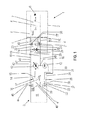
- FIG. 1 illustrates a construction generally designated by the reference numeral 1, which comprises an electrochromic device 2 and a circuit arrangement 3 electrically connected to the electrochromic device 2.
- the electrochromic device 2 is embodied here, for example, as electrochromic glazing with at least one transparent substrate (eg glass pane).
- An optical transparency of the electrochromic device 2 can be changed by applying an electric voltage and / or electrical current of suitable size and polarity, the electrochromic device 2 acting like a charge storage device with a reduction of the optical transparency.
- the electrochromic device 2 is illustrated by their (dashed outlined) equivalent circuit diagram. Accordingly, the electrochromic device 2 has in its capacity as a charge storage device an electrical capacitor 5 which can be charged or discharged via the two device connections 9, 10. Depending on the specific structure of the electrochromic device 2, the capacitance 5 can be charged only by applying a suitably (properly) poled voltage, which in Fig. 1 is illustrated by a parallel to the capacitance 5 connected diode 6. As such, the two device terminals 9, 10 must be connected to the terminal terminals of an electric power source according to a specific terminal occupancy to desirably achieve coloration (reduction of optical transparency) or decoloration (increase in optical transparency) of the electrochromic device 2. With regard to the charge-storing property, coloring of the electrochromic device 2 results in an electric charge of the capacitor 5, while discoloration of the electrochromic device 2 results in a discharge of the capacitor 5.
- a leaking resistor 7 connected in parallel with the capacitor 5 indicates an ordinary manner of (low) self-discharge of the electrochromic device 2 due to leak and leakage currents.
- a terminal resistor 8 connected in series with the capacitor 5 indicates an electrical resistance of the lines for connecting the capacitor 5 to the device terminals 9, 10.
- the capacity of the electrochromic glazing with a contrast of 20 may be about 300 F / m 2 .
- the leakage resistance 7 can amount to approximately 20 ohms for a glazing with an area of 1 m 2 .
- the connection resistance 8 can be approx. 0.5 ohms.
- the circuit arrangement 3 comprises a control device 11 for controlling various components of the circuit arrangement 3. It further comprises a controllable first electrical power source (voltage / current source) 12 and a non-controllable second electrical power source (voltage / current source) 13, by which the electrochromic Device 2 electrical power (DC electrical and / or electrical DC) can be supplied.
- the two power sources 12, 13 are alternately electrically conductively connected to the two device terminals 9, 10 with the interposition of a Polklemmen facialscrien 4 alternately.
- the two power sources 12, 13 are each provided with two pole terminals, wherein a pole terminal of the same name of the two power sources 12, 13 is short-circuited to a common, third pole terminal 16.
- the first power source 12 is provided with a first pole terminal 14 and the third pole terminal 16, the second voltage source 13 with a second pole terminal 15 and the third pole terminal 16.
- the first power source 12 serves to reduce the optical transparency of the electrochromic device 2, while the second power source 13 serves to increase the optical transparency of the electrochromic device 2.
- the two power sources 12, 13 have for this purpose a maximum DC voltage or maximum DC which is adapted to the respective function, wherein a maximum DC voltage or maximum direct current of the second power source 13 is usually less than a maximum DC voltage or maximum DC current of the first power source 12 is.
- either the first pole terminal 14 of the first power source 12 or the second pole terminal 15 of the second power source 13 can be electrically connected to the first device terminal 9 of the electrochromic device 2 via a first connecting line 18.
- the (common) third pole terminal 16 of the two power sources 12, 13 can be electrically conductively connected to the second device terminal 10 of the electrochromic device 2 via a second connecting line 19.
- Both the first connecting line 18 and the second connecting line 19 are part of the pole terminal switching circuit 4, which in Fig. 1 shown outlined by dashed lines.
- the pole terminal switching circuit 4 comprises, in addition to the first connecting line 18 and the second connecting line 19, a first transistor pair having a first transistor 20 and a second transistor 21, each designed as controllable field effect transistors, each transistor having a load path (ie a source and drain -Connection of the transistor interconnecting current path) and a control terminal for controlling the current flow in the load path.
- a load path of the first transistor 20 divide the first lead 18 into a first terminal-side portion 47 and a first terminal-side portion 48 and a load path of the second transistor 21, the second terminal lead 19 into a second terminal-side portion 49 and a second terminal-side portion 50.
- the pole terminal switching circuit 4 further includes a first bridge line 22 through which the first terminal side portion 47 is electrically conductively connectable to the second terminal side portion 50, and a second bridge line 23 through which the second terminal side portion 49 is electrically conductively connected to the first terminal side portion 48 is.
- the Polklemmen facialscnies 4 comprises a second pair of transistors having a third transistor 24 and a fourth transistor 25, which are each designed as controllable field effect transistors, wherein a load path of the third transistor 24 in the first bridge line 22 and a load path of the fourth transistor 25 in the second bridge line 23 are included.
- a first control terminal 26 of the first transistor 20 and a second control terminal 27 of the second transistor 21 are connected via a common first control line 30 connected to a first signal output 32 of the control device 11, so that the control device 11 with the interposition of a first amplifier 34 control signals for simultaneous control of the two transistors 20, 21 to the first control terminal 26 and the second control terminal 27 can transmit.
- a third control terminal 28 of the third transistor 24 and a fourth control terminal 29 of the fourth transistor 25 are connected via a common second control line 31 to a second signal output 33 of the control device 11, so that the control device 11 with the interposition of a second amplifier 35 control signals simultaneously to the third Control terminal 28 and the fourth control terminal 29 can transmit.
- an electric current in the load path controlled by the control terminal can be transmitted or blocked by means of a field effect.
- a grounded actuator 36 for example, solenoid
- the controllable first power source 12 is connected via a fourth control line 41 to a fourth signal output (A / D output) 40 of the control device 11 in terms of data technology.
- the controller 11 may generate and provide control signals at the fourth signal output 40, which are transmitted via the fourth control line 41 to the first power source 12 to control a maximum voltage or current. Due to the size of the maximum voltage or maximum current, the optical transparency of the electrochromic device 2 can be reduced to a desired transparency value.
- the control device 11 is furthermore provided with an integrated voltage / current measuring device 46, which has a first signal input 44 (A / D input) and a first measuring line 42 connected thereto, as well as a second signal input 45 (A / D input). and a second measuring line 43 connected thereto is electrically conductively connected to the two device terminals 9, 10 of the electrochromic device 2.
- the voltage / current measuring device 46 may measure a DC electrical voltage and / or a DC electrical current (including signs) between the two device terminals 9, 10.
- a machine-readable program code is implemented, by which, in particular before the first electrical connection of the electrochromic device 2 to the first power source 12, a DC electrical voltage (including its sign) at the two device terminals 9, 10 by means of voltage / Current measuring device 46 is measured. A measurement of the electrical voltage or the electric current takes place when no electrical power of the electrochromic device 2 is supplied.
- a first variant is considered, in which the electrochromic device 2 has a reduced optical transparency, so that a DC electrical voltage can be measured at the two device terminals 9, 10 on the basis of their charge storage capacity.
- the sign (polarity) of the measured electrical quantity is compared with the polarity of the first power source 12 and the first power source 12 is electrically connected to the device terminals 9, 10, the polarity of the first power source 12 is equal to the polarity of the measured electrical quantity.
- the first pole terminal 14 has a higher potential than the third pole terminal 15, the first terminal post 14 with the first device terminal 9 and the third pole terminal 16 to the second device terminal 10 electrically conductively connected.
- the first pair of transistors with the first transistor 20 and the second transistor 21 are switched to passage, while the second pair of transistors with the third transistor 24 and the fourth transistor 25 is turned off.
- the third pole terminal 16 becomes first device terminal 9 and the first pole terminal 14 to the second device terminal 10 electrically conductively connected.
- the first transistor pair with the first transistor 20 and the second transistor 21 is turned off, while the second transistor pair with the third transistor 24 and the fourth transistor 25 is switched to passage.
- a second variant is considered, in which the electrochromic device 2 does not have reduced optical transparency, so that no DC electrical voltage is generated at the two device terminals 9, 10.
- the first power source 12 is electrically conductively connected to the two device terminals 9, 10 for a selectable period of time (hereinafter referred to as "charging step" for ease of reference).
- the magnitude of the DC voltage or current applied to the two device terminals during the charging step is chosen such that a maximum permissible DC voltage or DC of the electrochromic device 2 is not exceeded.
- the first power source 12 is separated again from the electrochromic device 2, which can be achieved by blocking the transistors.
- the sign (polarity) of the measured electrical variable with the polarity of the first power source 12 is compared and the first power source 12 so with the device terminals 9, 10 electrically conductively connected so that the polarity of the first power source 12 is equal to the polarity of the measured electrical quantity.
- the polarity of the two pole terminals 14, 16 of the first power source 12 corresponds to the polarity in the charging step, since only then can a reduction in the optical transparency of the electrochromic device 2 be achieved.
- the pole terminals 14, 16 of the first power source 12 are electrically connected to the device terminals 9, 10, that their polarity to the polarity of the pole terminals 14, 16 is reversed at the charging step.
- the first device terminal 9 becomes electrically connected to the third pole terminal 16 and the second device terminal 10 to the first terminal post 14 conductively connected.
- the first transistor pair with the first transistor 20 and the second transistor 21 is turned off, while the second transistor pair with the third transistor 24 and the fourth transistor 25 is switched to passage.
- the charging step when the first device terminal 9 is electrically conductively connected to the third pole terminal 16 and the second device terminal 10 is electrically connected to the first pole terminal 14, the first device terminal 9 with the first terminal post 14 and the second terminal device 10 with the third pole terminal 16 electrically connected.
- the first pair of transistors with the first transistor 20 and the second transistor 21 are switched to passage, while the second pair of transistors with the third transistor 24 and the fourth transistor 25 is turned off.
- the optical transparency of the electrochromic device 2 under the control of the controller 11 can be desirably reduced.
- the optical transparency of the electrochromic device 2 can be increased.
- the structure 1 according to the invention thus advantageously makes it possible to adapt the polarity of the first power source 12 used to reduce the optical transparency or the second power source 13 used to increase the optical transparency to the polarity of the electrochromic device 2. In this way, a desired control the optical transparency of the electrochromic device 2 ensured and damage by incorrect application of too high DC voltage or high direct current can be reliably avoided.
- two power sources 12, 13 are used, with the first power source 12 for reducing the optical transparency and the second power source 13 for increasing the optical transparency, it would be equally conceivable to provide only a single power source, for example the first power source 12, and a To increase the optical transparency of the electrochromic device 2 by shorting the two device ports 9, 10 to achieve. This can be achieved, for example, by switching all four transistors on, whereby, for example, an additional controllable transistor would have to be provided in the second connecting line 19.
Landscapes
- Physics & Mathematics (AREA)
- Nonlinear Science (AREA)
- General Physics & Mathematics (AREA)
- Optics & Photonics (AREA)
- Electrochromic Elements, Electrophoresis, Or Variable Reflection Or Absorption Elements (AREA)
- Control Of Indicators Other Than Cathode Ray Tubes (AREA)
Claims (12)
- Montage (1) comprenant un dispositif électrochrome (2) muni de deux connexions de dispositif (9, 10) et une structure de circuit (3), la structure de circuit (3) présentant :- un dispositif de mesure de tension/courant (46) relié aux deux connexions de dispositif (9, 10) ;- au moins une source de puissance électrique (12) munie de deux bornes polaires (14, 16), qui est connectée aux deux connexions de dispositif (9, 10) par l'intermédiaire d'un circuit (4) d'inversion des bornes polaires pouvant être commandé, une connexion de dispositif pouvant être reliée électriquement sélectivement à l'une des deux bornes polaires, et l'autre connexion de dispositif en même temps reliée électriquement à l'autre borne polaire, par le circuit (4) d'inversion de bornes polaires ;- un dispositif de commande électronique (11) qui est destiné à commander le circuit (4) d'inversion des bornes polaires et qui est conçu de manière qu'une tension électrique et/ou un courant électrique soit ou soient mesuré(s) entre les connexions de dispositif (9, 10) et que les connexions de dispositif (9, 10) soient respectivement reliées aux bornes polaires (14, 16) de manière qu'une polarité de la grandeur électrique mesurée aux connexions de dispositif (9, 10) corresponde à une polarité de la source de puissance électrique (12).
- Montage (1) selon la revendication 1, caractérisé par le fait que le dispositif de commande (11) est conçu de manière que de la puissance électrique soit appliquée au dispositif électrochrome (2) pendant un laps de temps pouvant être choisi, dans le cas où aucune tension ne peut être mesurée entre les connexions de dispositif (9, 10), où- dans le cas où, après écoulement du laps de temps, une tension électrique et/ou un courant électrique est ou sont mesuré(s) entre les connexions de dispositif (9, 10), les connexions de dispositif (9, 10) sont reliées respectivement aux bornes polaires (14, 16) de manière qu'une polarité de la grandeur électrique mesurée aux connexions de dispositif (9, 10) corresponde à une polarité de la source de puissance électrique (12), et- dans le cas où, après écoulement du laps de temps, aucune tension électrique ni aucun courant électrique n'est mesuré entre les connexions de dispositif (9, 10), les connexions de dispositif sont reliées respectivement aux bornes polaires (14, 16) de manière que la polarité des bornes polaires soit inversée par rapport à la polarité des bornes polaires existant lors de l'application de la puissance électrique.
- Montage (1) selon l'une des revendications 1 à 2, caractérisé par le fait que le dispositif de mesure de tension/courant (46) est intégré dans le dispositif de commande (11).
- Montage (1) selon l'une des revendications 1 à 3, caractérisé par le fait que le circuit (4) d'inversion de bornes polaires comprend :- un premier conducteur de connexion (18) par lequel une première borne polaire (14) de la source de puissance (12) est apte à être reliée électriquement à une première connexion de dispositif (9) ;- un second conducteur de connexion (19) par lequel une seconde borne polaire (15) de la source de puissance (12) est apte à être reliée électriquement à une seconde connexion de dispositif (10) ;- une première paire de transistors comprenant un premier transistor (20) et un deuxième transistor (21 où un trajet de charge du premier transistor (20) divise le premier conducteur de connexion (18) en un premier segment côté borne (47) et un premier segment côté connexion (48) et un trajet de charge du deuxième transistor (21) divise le second conducteur de connexion (19) en un second segment côté borne (49) et un second segment côté connexion (50) ;- un premier conducteur de pont (22) par lequel le premier segment côté borne (47) est apte à être relié électriquement au second segment côté connexion (50) ;- un second conducteur de pont (23) par lequel le second segment côté borne (49) est apte à être relié électriquement au premier segment côté connexion (48) ;- une seconde paire de transistors comprenant un troisième transistor (24) et un quatrième transistor (25), où un trajet de charge du troisième transistor (24) est contenu dans le premier conducteur de pont (22) et un trajet de charge du quatrième transistor (25) est contenu dans le second conducteur de pont (23), et des connexions de commande (26-29) des transistors sont reliées au dispositif de commande électronique (11).
- Montage (1) selon la revendication 4, caractérisé par le fait que les connexions de commande (26, 27 ; 28, 29) des transistors d'une paire de transistors respective (20, 21 ; 24, 25) sont reliées à une sortie de signal commune (32, 33) du dispositif de commande électronique (11).
- Montage (1) selon l'une des revendications 1 à 5, caractérisé par le fait qu'il comprend une première source de puissance électrique (12) et une seconde source de puissance électrique (13) qui sont connectées respectivement aux connexions de dispositif (9, 10) au moyen du circuit (4) d'inversion de bornes polaires, les bornes polaires des deux source de puissance étant aptes à être reliées sélectivement aux connexions de dispositif sous l'effet de la commande d'un commutateur inverseur (17).
- Montage (1) selon la revendication 6, caractérisé par le fait que le commutateur inverseur (17) est apte à être commandé par le dispositif de commande électronique (11).
- Montage (1) selon l'une des revendications 6 à 7, caractérisé par le fait qu'une tension de sortie maximum ou un courant de sortie maximum d'au moins l'une des deux sources de puissance électrique (12) est apte à être réglé par le dispositif de commande électronique (11).
- Montage (1) selon l'une des revendications 1 à 8, caractérisé par le fait que le dispositif électrochrome (2) est un vitrage électrochrome comprenant au moins un substrat transparent.
- Procédé pour adapter la polarité d'une source de puissance électrique à la polarité d'un dispositif électrochrome, caractérisé par les étapes suivantes :- mesure d'une tension électrique ou d'un courant électrique entre des connexions de dispositif du dispositif électrochrome au moyen d'un dispositif de mesure de tension/courant ;- comparaison de la polarité de la grandeur électrique mesurée à la polarité de la source de puissance au moyen d'un dispositif de commande électronique ;- mise en liaison électrique des bornes de dispositif avec les bornes polaires au moyen d'un circuit inverseur des bornes polaires commandé par le dispositif de commande, les connexions de dispositif étant reliées aux bornes polaires de manière qu'une polarité de la grandeur électrique mesurée aux bornes polaires corresponde à la polarité de la source de puissance électrique.
- Procédé selon la revendication 10, caractérisé par le fait qu'une puissance électrique est appliquée au dispositif électrochrome pendant un laps de temps pouvant être choisi, dans le cas où aucune tension électrique ni aucun courant électrique ne peut être mesuré entre les connexions de dispositif, où- dans le cas où, après écoulement du laps de temps, une tension électrique ou un courant électrique est mesuré entre les connexions de dispositif, les connexions de dispositif sont reliées respectivement aux bornes polaires de manière qu'une polarité de la tension mesurée aux bornes polaires corresponde à une polarité de la source de puissance électrique ; et- dans le cas où, après écoulement du laps de temps, aucune tension électrique ni aucun courant électrique n'est mesuré entre les connexions de dispositif, les connexions de dispositif sont reliées respectivement aux bornes polaires de manière que la polarité des bornes polaires soit inversée par rapport à la polarité des bornes polaires existant lors de l'application de la puissance électrique.
- Procédé d'utilisation d'un dispositif électrochrome, caractérisé par le fait qu'avant de modifier la transparence optique du dispositif électrochrome au moyen d'une source d'énergie électrique, on met en oeuvre un procédé d'adaptation de la polarité de la source de puissance électrique à la polarité du dispositif électrochrome selon l'une des revendications 10 à 11.
Applications Claiming Priority (2)
| Application Number | Priority Date | Filing Date | Title |
|---|---|---|---|
| DE102008061403A DE102008061403B4 (de) | 2008-12-10 | 2008-12-10 | Aufbau und Verfahren zum Anpassen der Polarität einer Leistungsquelle an eine elektrochrome Vorrichtung |
| PCT/EP2009/064059 WO2010066499A1 (fr) | 2008-12-10 | 2009-10-26 | Structure et procédé pour adapter la polarité d'une source de puissance à un système électrochromique |
Publications (2)
| Publication Number | Publication Date |
|---|---|
| EP2364459A1 EP2364459A1 (fr) | 2011-09-14 |
| EP2364459B1 true EP2364459B1 (fr) | 2015-07-22 |
Family
ID=41435398
Family Applications (1)
| Application Number | Title | Priority Date | Filing Date |
|---|---|---|---|
| EP09752136.3A Not-in-force EP2364459B1 (fr) | 2008-12-10 | 2009-10-26 | Structure et procédé pour adapter la polarité d'une source de puissance à un système électrochromique |
Country Status (7)
| Country | Link |
|---|---|
| US (1) | US20110304898A1 (fr) |
| EP (1) | EP2364459B1 (fr) |
| JP (1) | JP5579739B2 (fr) |
| KR (1) | KR20110102326A (fr) |
| CN (1) | CN102246093A (fr) |
| DE (1) | DE102008061403B4 (fr) |
| WO (1) | WO2010066499A1 (fr) |
Families Citing this family (50)
| Publication number | Priority date | Publication date | Assignee | Title |
|---|---|---|---|---|
| US11314139B2 (en) | 2009-12-22 | 2022-04-26 | View, Inc. | Self-contained EC IGU |
| US10690540B2 (en) | 2015-10-06 | 2020-06-23 | View, Inc. | Multi-sensor having a light diffusing element around a periphery of a ring of photosensors |
| US8213074B1 (en) | 2011-03-16 | 2012-07-03 | Soladigm, Inc. | Onboard controller for multistate windows |
| EP3995885A1 (fr) | 2009-12-22 | 2022-05-11 | View, Inc. | Fenêtres électrochromiques alimentées sans fil |
| US11592723B2 (en) | 2009-12-22 | 2023-02-28 | View, Inc. | Automated commissioning of controllers in a window network |
| US20130271813A1 (en) | 2012-04-17 | 2013-10-17 | View, Inc. | Controller for optically-switchable windows |
| US11732527B2 (en) | 2009-12-22 | 2023-08-22 | View, Inc. | Wirelessly powered and powering electrochromic windows |
| US11342791B2 (en) | 2009-12-22 | 2022-05-24 | View, Inc. | Wirelessly powered and powering electrochromic windows |
| US10303035B2 (en) | 2009-12-22 | 2019-05-28 | View, Inc. | Self-contained EC IGU |
| US8705162B2 (en) | 2012-04-17 | 2014-04-22 | View, Inc. | Controlling transitions in optically switchable devices |
| US9778532B2 (en) | 2011-03-16 | 2017-10-03 | View, Inc. | Controlling transitions in optically switchable devices |
| US10935865B2 (en) | 2011-03-16 | 2021-03-02 | View, Inc. | Driving thin film switchable optical devices |
| US9645465B2 (en) | 2011-03-16 | 2017-05-09 | View, Inc. | Controlling transitions in optically switchable devices |
| US11822202B2 (en) | 2011-03-16 | 2023-11-21 | View, Inc. | Controlling transitions in optically switchable devices |
| US9454055B2 (en) | 2011-03-16 | 2016-09-27 | View, Inc. | Multipurpose controller for multistate windows |
| US9030725B2 (en) | 2012-04-17 | 2015-05-12 | View, Inc. | Driving thin film switchable optical devices |
| US9412290B2 (en) | 2013-06-28 | 2016-08-09 | View, Inc. | Controlling transitions in optically switchable devices |
| US8254013B2 (en) | 2011-03-16 | 2012-08-28 | Soladigm, Inc. | Controlling transitions in optically switchable devices |
| US11054792B2 (en) | 2012-04-13 | 2021-07-06 | View, Inc. | Monitoring sites containing switchable optical devices and controllers |
| US11630367B2 (en) | 2011-03-16 | 2023-04-18 | View, Inc. | Driving thin film switchable optical devices |
| EP2769042B1 (fr) | 2011-10-21 | 2018-02-21 | View, Inc. | Atténuation de choc thermique dans des fenêtres pouvant être colorées |
| US11950340B2 (en) | 2012-03-13 | 2024-04-02 | View, Inc. | Adjusting interior lighting based on dynamic glass tinting |
| US12578609B2 (en) | 2012-03-13 | 2026-03-17 | View Operating Corporation | Methods of controlling multi-zone tintable windows |
| US11635666B2 (en) | 2012-03-13 | 2023-04-25 | View, Inc | Methods of controlling multi-zone tintable windows |
| US10048561B2 (en) | 2013-02-21 | 2018-08-14 | View, Inc. | Control method for tintable windows |
| US12400651B2 (en) | 2012-04-13 | 2025-08-26 | View Operating Corporation | Controlling optically-switchable devices |
| US11674843B2 (en) | 2015-10-06 | 2023-06-13 | View, Inc. | Infrared cloud detector systems and methods |
| CN104335595B (zh) | 2012-04-13 | 2018-09-18 | 唯景公司 | 用于控制可光学切换的装置的应用 |
| US9638978B2 (en) | 2013-02-21 | 2017-05-02 | View, Inc. | Control method for tintable windows |
| US10964320B2 (en) | 2012-04-13 | 2021-03-30 | View, Inc. | Controlling optically-switchable devices |
| US11300848B2 (en) | 2015-10-06 | 2022-04-12 | View, Inc. | Controllers for optically-switchable devices |
| US11966142B2 (en) | 2013-02-21 | 2024-04-23 | View, Inc. | Control methods and systems using outside temperature as a driver for changing window tint states |
| US11960190B2 (en) | 2013-02-21 | 2024-04-16 | View, Inc. | Control methods and systems using external 3D modeling and schedule-based computing |
| US11719990B2 (en) | 2013-02-21 | 2023-08-08 | View, Inc. | Control method for tintable windows |
| US12372846B2 (en) | 2013-02-21 | 2025-07-29 | View Operating Corporation | Control methods and systems using external 3D modeling and schedule-based computing |
| US12422725B2 (en) | 2013-02-21 | 2025-09-23 | View Operating Corporation | Control methods and systems using outside temperature as a driver for changing window tint states |
| US12353111B2 (en) | 2013-06-28 | 2025-07-08 | View Operating Corporation | Controlling transitions in optically switchable devices |
| US10503039B2 (en) | 2013-06-28 | 2019-12-10 | View, Inc. | Controlling transitions in optically switchable devices |
| US9885935B2 (en) | 2013-06-28 | 2018-02-06 | View, Inc. | Controlling transitions in optically switchable devices |
| US12061404B2 (en) | 2013-06-28 | 2024-08-13 | View, Inc. | Controlling transitions in optically switchable devices |
| US10221612B2 (en) | 2014-02-04 | 2019-03-05 | View, Inc. | Infill electrochromic windows |
| CN112627704A (zh) | 2014-03-05 | 2021-04-09 | 唯景公司 | 监测含有可切换光学装置和控制器的站点 |
| US11114742B2 (en) | 2014-11-25 | 2021-09-07 | View, Inc. | Window antennas |
| TWI746446B (zh) | 2015-07-07 | 2021-11-21 | 美商唯景公司 | 用於可著色窗戶之控制方法 |
| US11255722B2 (en) | 2015-10-06 | 2022-02-22 | View, Inc. | Infrared cloud detector systems and methods |
| US10809587B2 (en) | 2015-10-06 | 2020-10-20 | View, Inc. | Controllers for optically-switchable devices |
| US11482147B2 (en) | 2016-04-29 | 2022-10-25 | View, Inc. | Calibration of electrical parameters in optically switchable windows |
| US11467464B2 (en) | 2017-04-26 | 2022-10-11 | View, Inc. | Displays for tintable windows |
| US11631493B2 (en) | 2020-05-27 | 2023-04-18 | View Operating Corporation | Systems and methods for managing building wellness |
| TW202206925A (zh) | 2020-03-26 | 2022-02-16 | 美商視野公司 | 多用戶端網路中之存取及傳訊 |
Family Cites Families (15)
| Publication number | Priority date | Publication date | Assignee | Title |
|---|---|---|---|---|
| JPS63107425U (fr) * | 1986-12-29 | 1988-07-11 | ||
| FR2629222B1 (fr) | 1988-03-25 | 1992-04-30 | Saint Gobain Vitrage | Vitrage a transmission variable du type electrochrome |
| JPS6438623U (fr) * | 1987-09-03 | 1989-03-08 | ||
| FR2649691B1 (fr) | 1989-07-11 | 1992-10-30 | Saint Gobain Vitrage Int | Vitrage electrochrome |
| FR2666804B1 (fr) * | 1990-09-14 | 1993-05-28 | Saint Gobain Vitrage Int | Vitrage electrochrome. |
| US5151824A (en) * | 1990-11-26 | 1992-09-29 | Donnelly Corporation | Vehicular outside mirror assembly |
| US5220317A (en) * | 1990-12-11 | 1993-06-15 | Donnelly Corporation | Electrochromic device capable of prolonged coloration |
| FR2706639B1 (fr) | 1993-06-11 | 1995-08-25 | Saint Gobain Vitrage Int | Vitrage électrochrome. |
| JP3249720B2 (ja) * | 1995-07-13 | 2002-01-21 | 株式会社村上開明堂 | 自動防眩ミラー |
| FR2753545B1 (fr) | 1996-09-18 | 1998-10-16 | Saint Gobain Vitrage | Dispositif electrochimique |
| DE19706918A1 (de) * | 1997-02-20 | 1998-08-27 | Flachglas Ag | Verfahren zum Betreiben eines elektrochromen Elementes |
| US6563339B2 (en) * | 2001-01-31 | 2003-05-13 | Micron Technology, Inc. | Multiple voltage supply switch |
| US20040001056A1 (en) * | 2002-06-28 | 2004-01-01 | Honeywell International Inc. | Electrochromic window driver |
| ATE366977T1 (de) * | 2003-09-19 | 2007-08-15 | Gesimat Gmbh Ges Fuer Intellig | Verfahren zur elektrischen ansteuerung von elektrochromen elementen |
| US7746534B2 (en) * | 2006-12-07 | 2010-06-29 | Gentex Corporation | Thin-film coatings, electro-optic elements and assemblies incorporating these elements |
-
2008
- 2008-12-10 DE DE102008061403A patent/DE102008061403B4/de not_active Expired - Fee Related
-
2009
- 2009-10-26 US US13/125,758 patent/US20110304898A1/en not_active Abandoned
- 2009-10-26 JP JP2011539981A patent/JP5579739B2/ja not_active Expired - Fee Related
- 2009-10-26 KR KR1020117013182A patent/KR20110102326A/ko not_active Ceased
- 2009-10-26 WO PCT/EP2009/064059 patent/WO2010066499A1/fr not_active Ceased
- 2009-10-26 EP EP09752136.3A patent/EP2364459B1/fr not_active Not-in-force
- 2009-10-26 CN CN2009801497131A patent/CN102246093A/zh active Pending
Also Published As
| Publication number | Publication date |
|---|---|
| DE102008061403A1 (de) | 2010-07-22 |
| WO2010066499A1 (fr) | 2010-06-17 |
| KR20110102326A (ko) | 2011-09-16 |
| US20110304898A1 (en) | 2011-12-15 |
| JP2012511737A (ja) | 2012-05-24 |
| DE102008061403B4 (de) | 2012-02-09 |
| CN102246093A (zh) | 2011-11-16 |
| JP5579739B2 (ja) | 2014-08-27 |
| EP2364459A1 (fr) | 2011-09-14 |
Similar Documents
| Publication | Publication Date | Title |
|---|---|---|
| EP2364459B1 (fr) | Structure et procédé pour adapter la polarité d'une source de puissance à un système électrochromique | |
| EP3503343A1 (fr) | Système électrique et procédé de diagnostic de la capacité de fonctionnement du relais de puissance dans un système électrique | |
| DE112013006752T5 (de) | LED-Hintergrundbeleuchtungstreiberschaltung und Hinterundbeleuchtungsmodul | |
| WO2010069697A1 (fr) | Vitrage optiquement actif pourvu d'une protection contre les surtensions | |
| EP2618439A2 (fr) | Circuit protecteur pour une batterie | |
| WO2013087604A1 (fr) | Circuit de détection de court-circuit dans un système de commutateurs de puissance | |
| EP2009765A2 (fr) | Dispositif d'alimentation en courant continue | |
| DE112018004725T5 (de) | Stromfluss-Steuereinrichtung | |
| DE102017213472A1 (de) | Verfahren zum Detektieren eines Fehlzustands einer Batterie, Batterie und Kraftfahrzeug | |
| EP1406143B1 (fr) | Procédé et dispositif de symétrisation des condensateurs d'une batterie de condensateurs | |
| DE102013205102B4 (de) | Erfassung des Zustands eines Akkumulatormoduls | |
| DE102021119956A1 (de) | Testen von Stromversorgungspfaden und Verbrauchern eines Fahrzeugs | |
| DE10343445A1 (de) | Verfahren zur elektrischen Ansteuerung von elektrochromen Elementen | |
| DE112017001341T5 (de) | Entladeschaltung und energiespeichereinrichtung | |
| DE102023102482B4 (de) | USB-Anschlusseinrichtung für ein Fahrzeug, Fahrzeug und Verfahren hierfür | |
| EP0888588B1 (fr) | Segment ou interface de bus pour connecter un module d'une commande programmable a un bus | |
| EP4049334A1 (fr) | Charge ou décharge de modules de batterie | |
| EP1517293B1 (fr) | Procédé de contrôle életrique de vitrage électrochrome | |
| DE102024102649B4 (de) | Hochvoltverbinder mit vorladewiderstand und elektrofahrzeug | |
| DE202015103339U1 (de) | Schaltungsanordnung für einen sicheren digitalen Schaltausgang | |
| DE202015102462U1 (de) | Überspannungs-und Verpolschutz für LED-Module im Fahrzeug | |
| WO2020011439A1 (fr) | Procédé et dispositif destinés à faire fonctionner un moteur électrique pour un équipement de frein électrique | |
| DE102023202812A1 (de) | Elektrische Ladeeinrichtung für ein Fahrzeug und Verfahren zum Betreiben einer elektrischen Ladeeinrichtung | |
| DE102012214906A1 (de) | Steuergerät für elektrische Last | |
| WO2013107592A2 (fr) | Dispositif et procédé permettant de déterminer l'établissement réussi du contact dans une connexion |
Legal Events
| Date | Code | Title | Description |
|---|---|---|---|
| PUAI | Public reference made under article 153(3) epc to a published international application that has entered the european phase |
Free format text: ORIGINAL CODE: 0009012 |
|
| 17P | Request for examination filed |
Effective date: 20110323 |
|
| AK | Designated contracting states |
Kind code of ref document: A1 Designated state(s): AT BE BG CH CY CZ DE DK EE ES FI FR GB GR HR HU IE IS IT LI LT LU LV MC MK MT NL NO PL PT RO SE SI SK SM TR |
|
| DAX | Request for extension of the european patent (deleted) | ||
| RAP1 | Party data changed (applicant data changed or rights of an application transferred) |
Owner name: SAGE ELECTROCHROMICS, INC. |
|
| GRAP | Despatch of communication of intention to grant a patent |
Free format text: ORIGINAL CODE: EPIDOSNIGR1 |
|
| INTG | Intention to grant announced |
Effective date: 20150415 |
|
| GRAS | Grant fee paid |
Free format text: ORIGINAL CODE: EPIDOSNIGR3 |
|
| GRAA | (expected) grant |
Free format text: ORIGINAL CODE: 0009210 |
|
| AK | Designated contracting states |
Kind code of ref document: B1 Designated state(s): AT BE BG CH CY CZ DE DK EE ES FI FR GB GR HR HU IE IS IT LI LT LU LV MC MK MT NL NO PL PT RO SE SI SK SM TR |
|
| REG | Reference to a national code |
Ref country code: GB Ref legal event code: FG4D Free format text: NOT ENGLISH |
|
| REG | Reference to a national code |
Ref country code: CH Ref legal event code: EP |
|
| REG | Reference to a national code |
Ref country code: IE Ref legal event code: FG4D Free format text: LANGUAGE OF EP DOCUMENT: GERMAN |
|
| REG | Reference to a national code |
Ref country code: AT Ref legal event code: REF Ref document number: 738232 Country of ref document: AT Kind code of ref document: T Effective date: 20150815 |
|
| REG | Reference to a national code |
Ref country code: DE Ref legal event code: R096 Ref document number: 502009011291 Country of ref document: DE |
|
| REG | Reference to a national code |
Ref country code: FR Ref legal event code: PLFP Year of fee payment: 7 |
|
| PGFP | Annual fee paid to national office [announced via postgrant information from national office to epo] |
Ref country code: FR Payment date: 20150908 Year of fee payment: 7 |
|
| REG | Reference to a national code |
Ref country code: LT Ref legal event code: MG4D |
|
| REG | Reference to a national code |
Ref country code: NL Ref legal event code: MP Effective date: 20150722 |
|
| PG25 | Lapsed in a contracting state [announced via postgrant information from national office to epo] |
Ref country code: LT Free format text: LAPSE BECAUSE OF FAILURE TO SUBMIT A TRANSLATION OF THE DESCRIPTION OR TO PAY THE FEE WITHIN THE PRESCRIBED TIME-LIMIT Effective date: 20150722 Ref country code: NO Free format text: LAPSE BECAUSE OF FAILURE TO SUBMIT A TRANSLATION OF THE DESCRIPTION OR TO PAY THE FEE WITHIN THE PRESCRIBED TIME-LIMIT Effective date: 20151022 Ref country code: FI Free format text: LAPSE BECAUSE OF FAILURE TO SUBMIT A TRANSLATION OF THE DESCRIPTION OR TO PAY THE FEE WITHIN THE PRESCRIBED TIME-LIMIT Effective date: 20150722 Ref country code: LV Free format text: LAPSE BECAUSE OF FAILURE TO SUBMIT A TRANSLATION OF THE DESCRIPTION OR TO PAY THE FEE WITHIN THE PRESCRIBED TIME-LIMIT Effective date: 20150722 Ref country code: GR Free format text: LAPSE BECAUSE OF FAILURE TO SUBMIT A TRANSLATION OF THE DESCRIPTION OR TO PAY THE FEE WITHIN THE PRESCRIBED TIME-LIMIT Effective date: 20151023 |
|
| PGFP | Annual fee paid to national office [announced via postgrant information from national office to epo] |
Ref country code: GB Payment date: 20151021 Year of fee payment: 7 Ref country code: DE Payment date: 20151020 Year of fee payment: 7 |
|
| PG25 | Lapsed in a contracting state [announced via postgrant information from national office to epo] |
Ref country code: SE Free format text: LAPSE BECAUSE OF FAILURE TO SUBMIT A TRANSLATION OF THE DESCRIPTION OR TO PAY THE FEE WITHIN THE PRESCRIBED TIME-LIMIT Effective date: 20150722 Ref country code: IS Free format text: LAPSE BECAUSE OF FAILURE TO SUBMIT A TRANSLATION OF THE DESCRIPTION OR TO PAY THE FEE WITHIN THE PRESCRIBED TIME-LIMIT Effective date: 20151122 Ref country code: PT Free format text: LAPSE BECAUSE OF FAILURE TO SUBMIT A TRANSLATION OF THE DESCRIPTION OR TO PAY THE FEE WITHIN THE PRESCRIBED TIME-LIMIT Effective date: 20151123 Ref country code: ES Free format text: LAPSE BECAUSE OF FAILURE TO SUBMIT A TRANSLATION OF THE DESCRIPTION OR TO PAY THE FEE WITHIN THE PRESCRIBED TIME-LIMIT Effective date: 20150722 Ref country code: HR Free format text: LAPSE BECAUSE OF FAILURE TO SUBMIT A TRANSLATION OF THE DESCRIPTION OR TO PAY THE FEE WITHIN THE PRESCRIBED TIME-LIMIT Effective date: 20150722 Ref country code: PL Free format text: LAPSE BECAUSE OF FAILURE TO SUBMIT A TRANSLATION OF THE DESCRIPTION OR TO PAY THE FEE WITHIN THE PRESCRIBED TIME-LIMIT Effective date: 20150722 |
|
| REG | Reference to a national code |
Ref country code: DE Ref legal event code: R097 Ref document number: 502009011291 Country of ref document: DE |
|
| PG25 | Lapsed in a contracting state [announced via postgrant information from national office to epo] |
Ref country code: SK Free format text: LAPSE BECAUSE OF FAILURE TO SUBMIT A TRANSLATION OF THE DESCRIPTION OR TO PAY THE FEE WITHIN THE PRESCRIBED TIME-LIMIT Effective date: 20150722 Ref country code: IT Free format text: LAPSE BECAUSE OF FAILURE TO SUBMIT A TRANSLATION OF THE DESCRIPTION OR TO PAY THE FEE WITHIN THE PRESCRIBED TIME-LIMIT Effective date: 20150722 Ref country code: EE Free format text: LAPSE BECAUSE OF FAILURE TO SUBMIT A TRANSLATION OF THE DESCRIPTION OR TO PAY THE FEE WITHIN THE PRESCRIBED TIME-LIMIT Effective date: 20150722 Ref country code: DK Free format text: LAPSE BECAUSE OF FAILURE TO SUBMIT A TRANSLATION OF THE DESCRIPTION OR TO PAY THE FEE WITHIN THE PRESCRIBED TIME-LIMIT Effective date: 20150722 Ref country code: CZ Free format text: LAPSE BECAUSE OF FAILURE TO SUBMIT A TRANSLATION OF THE DESCRIPTION OR TO PAY THE FEE WITHIN THE PRESCRIBED TIME-LIMIT Effective date: 20150722 |
|
| PLBE | No opposition filed within time limit |
Free format text: ORIGINAL CODE: 0009261 |
|
| STAA | Information on the status of an ep patent application or granted ep patent |
Free format text: STATUS: NO OPPOSITION FILED WITHIN TIME LIMIT |
|
| PG25 | Lapsed in a contracting state [announced via postgrant information from national office to epo] |
Ref country code: RO Free format text: LAPSE BECAUSE OF FAILURE TO SUBMIT A TRANSLATION OF THE DESCRIPTION OR TO PAY THE FEE WITHIN THE PRESCRIBED TIME-LIMIT Effective date: 20150722 Ref country code: LU Free format text: LAPSE BECAUSE OF FAILURE TO SUBMIT A TRANSLATION OF THE DESCRIPTION OR TO PAY THE FEE WITHIN THE PRESCRIBED TIME-LIMIT Effective date: 20151026 |
|
| REG | Reference to a national code |
Ref country code: CH Ref legal event code: PL |
|
| 26N | No opposition filed |
Effective date: 20160425 |
|
| PG25 | Lapsed in a contracting state [announced via postgrant information from national office to epo] |
Ref country code: MC Free format text: LAPSE BECAUSE OF FAILURE TO SUBMIT A TRANSLATION OF THE DESCRIPTION OR TO PAY THE FEE WITHIN THE PRESCRIBED TIME-LIMIT Effective date: 20150722 |
|
| REG | Reference to a national code |
Ref country code: IE Ref legal event code: MM4A |
|
| PG25 | Lapsed in a contracting state [announced via postgrant information from national office to epo] |
Ref country code: CH Free format text: LAPSE BECAUSE OF NON-PAYMENT OF DUE FEES Effective date: 20151031 Ref country code: LI Free format text: LAPSE BECAUSE OF NON-PAYMENT OF DUE FEES Effective date: 20151031 |
|
| PG25 | Lapsed in a contracting state [announced via postgrant information from national office to epo] |
Ref country code: SI Free format text: LAPSE BECAUSE OF FAILURE TO SUBMIT A TRANSLATION OF THE DESCRIPTION OR TO PAY THE FEE WITHIN THE PRESCRIBED TIME-LIMIT Effective date: 20150722 |
|
| PG25 | Lapsed in a contracting state [announced via postgrant information from national office to epo] |
Ref country code: IE Free format text: LAPSE BECAUSE OF NON-PAYMENT OF DUE FEES Effective date: 20151026 |
|
| REG | Reference to a national code |
Ref country code: AT Ref legal event code: MM01 Ref document number: 738232 Country of ref document: AT Kind code of ref document: T Effective date: 20151026 |
|
| PG25 | Lapsed in a contracting state [announced via postgrant information from national office to epo] |
Ref country code: AT Free format text: LAPSE BECAUSE OF NON-PAYMENT OF DUE FEES Effective date: 20151026 |
|
| REG | Reference to a national code |
Ref country code: DE Ref legal event code: R119 Ref document number: 502009011291 Country of ref document: DE |
|
| PG25 | Lapsed in a contracting state [announced via postgrant information from national office to epo] |
Ref country code: BG Free format text: LAPSE BECAUSE OF FAILURE TO SUBMIT A TRANSLATION OF THE DESCRIPTION OR TO PAY THE FEE WITHIN THE PRESCRIBED TIME-LIMIT Effective date: 20150722 Ref country code: SM Free format text: LAPSE BECAUSE OF FAILURE TO SUBMIT A TRANSLATION OF THE DESCRIPTION OR TO PAY THE FEE WITHIN THE PRESCRIBED TIME-LIMIT Effective date: 20150722 Ref country code: HU Free format text: LAPSE BECAUSE OF FAILURE TO SUBMIT A TRANSLATION OF THE DESCRIPTION OR TO PAY THE FEE WITHIN THE PRESCRIBED TIME-LIMIT; INVALID AB INITIO Effective date: 20091026 |
|
| GBPC | Gb: european patent ceased through non-payment of renewal fee |
Effective date: 20161026 |
|
| PG25 | Lapsed in a contracting state [announced via postgrant information from national office to epo] |
Ref country code: CY Free format text: LAPSE BECAUSE OF FAILURE TO SUBMIT A TRANSLATION OF THE DESCRIPTION OR TO PAY THE FEE WITHIN THE PRESCRIBED TIME-LIMIT Effective date: 20150722 Ref country code: NL Free format text: LAPSE BECAUSE OF FAILURE TO SUBMIT A TRANSLATION OF THE DESCRIPTION OR TO PAY THE FEE WITHIN THE PRESCRIBED TIME-LIMIT Effective date: 20150722 |
|
| REG | Reference to a national code |
Ref country code: FR Ref legal event code: ST Effective date: 20170630 |
|
| PG25 | Lapsed in a contracting state [announced via postgrant information from national office to epo] |
Ref country code: GB Free format text: LAPSE BECAUSE OF NON-PAYMENT OF DUE FEES Effective date: 20161026 Ref country code: BE Free format text: LAPSE BECAUSE OF NON-PAYMENT OF DUE FEES Effective date: 20151031 Ref country code: DE Free format text: LAPSE BECAUSE OF NON-PAYMENT OF DUE FEES Effective date: 20170503 Ref country code: FR Free format text: LAPSE BECAUSE OF NON-PAYMENT OF DUE FEES Effective date: 20161102 |
|
| PG25 | Lapsed in a contracting state [announced via postgrant information from national office to epo] |
Ref country code: TR Free format text: LAPSE BECAUSE OF FAILURE TO SUBMIT A TRANSLATION OF THE DESCRIPTION OR TO PAY THE FEE WITHIN THE PRESCRIBED TIME-LIMIT Effective date: 20150722 Ref country code: MT Free format text: LAPSE BECAUSE OF FAILURE TO SUBMIT A TRANSLATION OF THE DESCRIPTION OR TO PAY THE FEE WITHIN THE PRESCRIBED TIME-LIMIT Effective date: 20150722 |
|
| PG25 | Lapsed in a contracting state [announced via postgrant information from national office to epo] |
Ref country code: MK Free format text: LAPSE BECAUSE OF FAILURE TO SUBMIT A TRANSLATION OF THE DESCRIPTION OR TO PAY THE FEE WITHIN THE PRESCRIBED TIME-LIMIT Effective date: 20150722 |