EP2365521A2 - Paquet de niveau de tranche à couche mince - Google Patents
Paquet de niveau de tranche à couche mince Download PDFInfo
- Publication number
- EP2365521A2 EP2365521A2 EP11075009A EP11075009A EP2365521A2 EP 2365521 A2 EP2365521 A2 EP 2365521A2 EP 11075009 A EP11075009 A EP 11075009A EP 11075009 A EP11075009 A EP 11075009A EP 2365521 A2 EP2365521 A2 EP 2365521A2
- Authority
- EP
- European Patent Office
- Prior art keywords
- thin film
- anchor
- layer
- forming
- membrane
- Prior art date
- Legal status (The legal status is an assumption and is not a legal conclusion. Google has not performed a legal analysis and makes no representation as to the accuracy of the status listed.)
- Granted
Links
Images


Classifications
-
- B—PERFORMING OPERATIONS; TRANSPORTING
- B81—MICROSTRUCTURAL TECHNOLOGY
- B81B—MICROSTRUCTURAL DEVICES OR SYSTEMS, e.g. MICROMECHANICAL DEVICES
- B81B7/00—Microstructural systems ; Auxiliary parts of microstructural devices or systems
- B81B7/0032—Packages or encapsulation
- B81B7/0077—Other packages not provided for in groups B81B7/0035 - B81B7/0074
-
- B—PERFORMING OPERATIONS; TRANSPORTING
- B81—MICROSTRUCTURAL TECHNOLOGY
- B81B—MICROSTRUCTURAL DEVICES OR SYSTEMS, e.g. MICROMECHANICAL DEVICES
- B81B2207/00—Microstructural systems or auxiliary parts thereof
- B81B2207/01—Microstructural systems or auxiliary parts thereof comprising a micromechanical device connected to control or processing electronics, i.e. Smart-MEMS
- B81B2207/015—Microstructural systems or auxiliary parts thereof comprising a micromechanical device connected to control or processing electronics, i.e. Smart-MEMS the micromechanical device and the control or processing electronics being integrated on the same substrate
-
- B—PERFORMING OPERATIONS; TRANSPORTING
- B81—MICROSTRUCTURAL TECHNOLOGY
- B81C—PROCESSES OR APPARATUS SPECIALLY ADAPTED FOR THE MANUFACTURE OR TREATMENT OF MICROSTRUCTURAL DEVICES OR SYSTEMS
- B81C2203/00—Forming microstructural systems
- B81C2203/01—Packaging MEMS
- B81C2203/0136—Growing or depositing of a covering layer
-
- B—PERFORMING OPERATIONS; TRANSPORTING
- B81—MICROSTRUCTURAL TECHNOLOGY
- B81C—PROCESSES OR APPARATUS SPECIALLY ADAPTED FOR THE MANUFACTURE OR TREATMENT OF MICROSTRUCTURAL DEVICES OR SYSTEMS
- B81C2203/00—Forming microstructural systems
- B81C2203/01—Packaging MEMS
- B81C2203/0163—Reinforcing a cap, e.g. with ribs
-
- B—PERFORMING OPERATIONS; TRANSPORTING
- B81—MICROSTRUCTURAL TECHNOLOGY
- B81C—PROCESSES OR APPARATUS SPECIALLY ADAPTED FOR THE MANUFACTURE OR TREATMENT OF MICROSTRUCTURAL DEVICES OR SYSTEMS
- B81C2203/00—Forming microstructural systems
- B81C2203/07—Integrating an electronic processing unit with a micromechanical structure
- B81C2203/0707—Monolithic integration, i.e. the electronic processing unit is formed on or in the same substrate as the micromechanical structure
- B81C2203/0714—Forming the micromechanical structure with a CMOS process
-
- B—PERFORMING OPERATIONS; TRANSPORTING
- B81—MICROSTRUCTURAL TECHNOLOGY
- B81C—PROCESSES OR APPARATUS SPECIALLY ADAPTED FOR THE MANUFACTURE OR TREATMENT OF MICROSTRUCTURAL DEVICES OR SYSTEMS
- B81C2203/00—Forming microstructural systems
- B81C2203/07—Integrating an electronic processing unit with a micromechanical structure
- B81C2203/0707—Monolithic integration, i.e. the electronic processing unit is formed on or in the same substrate as the micromechanical structure
- B81C2203/0735—Post-CMOS, i.e. forming the micromechanical structure after the CMOS circuit
Definitions
- the present disclosure is related to thin film wafer level package and a method for forming such thin film wafer level package.
- MEM Micro Electro Mechanical
- poly-SiGe both as a structural material for the MEM device and as the thin film packaging layer enables the integration of a packaged MEM device on a CMOS substrate thanks to the low deposition temperature of the poly-SiGe ( ⁇ 450°C).
- the shear strength of the package is very important.
- the disclosure is related to thin film packages, i.e. 0-level package, having different anchor design parameters, processing parameters and using different release processes.
- Preferably SiGe is used to form the thin film package.
- the invention is related to a thin film package, method and microelectronic device as disclosed in the appended claims.
- the invention is related to a thin film wafer level package comprising a substrate, a membrane and an anchor frame configured to support the membrane and to connect the membrane to the substrate, said anchor frame having an inner wall and an outer wall, thereby forming within said inner wall a chamber between the substrate and the membrane, wherein the anchor frame comprises at least one cavity or at least one group of cavities between said inner and outer walls, said cavity or group of cavities encircling the chamber.
- encircling is meant that either at least one cavity forms a closed loop around the chamber area, or a number of cavities are placed at a plurality of places all around the chamber area.
- the cavity or cavities may be empty openings (i.e. not filled with solid material) or openings filled with a solid material different from the anchor frame material.
- the anchor frame comprises at least two closed-loop walls, a cavity being formed by the spacing between two adjacent closed-loop walls.
- the closed-loop walls may be concentric. They may have the same width.
- the cavity may be configured as a grid of cavities, possibly interconnected cavities.
- the membrane and the anchor frame may be formed of the same material. According to a preferred embodiment, this material is silicon-germanium.
- the at least one cavity or group of cavities in the anchor frame is filled with a material different from the material of the anchor frame.
- Said material may be silicon-oxide.
- the invention is equally related to a microelectronic device comprising a thin film wafer level package according to the invention.
- the thin film wafer level package encapsulates a MEM device contained in the chamber.
- the invention is equally related to a method of forming a thin film wafer level package on a substrate, the method comprising:
- the method may further comprise forming a Ti-TiN interlayer on the sacrificial layer and on the filled trenches before forming the membrane layer.
- the method may further comprise a soft sputter etch step prior to the formation of a Ti-TiN interlayer.
- forming at least two closed-loop trenches comprises forming a plurality of trenches connecting these closed-loop trenches. According to an embodiment, forming at least two closed-loop trenches comprises forming a plurality of trenches between and separate from these closed-loop trenches.
- the filling layer and the overlying layer may be formed simultaneously.
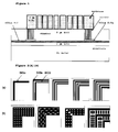
- Figure 1 shows a schematic cross-section of a thin film wafer level package, according to this disclosure, before release of the MEM device within the package with release holes in the SiGe membrane overlying the sacrificial SiO2 layer surrounding the MEM device.
- Figures 2 (a) and (b) shows examples of different anchor designs for the thin film wafer level package according to this disclosure: (a) the cavities in the SiGe frame are formed as continuous lines (b) the cavities in the SiGe frame are formed as grid of, optionally interconnected, cavities.
- the grey lines are the poly-SiGe walls of the SiGe frame, while the white color represents the cavities within this SiGe frame which are here filled with SiO 2.
- Figure 3 shows a shear force test measurement performed on 10 different thin wafer film packages according to this disclosure.
- the peak height gives the required force to destroy the package.
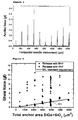
- Figure 4 shows the shear force values for different anchor designs, according to this disclosure, released using a wet (dark triangle) or dry (grey star) release process of the encapsulated MEM device. Also the MIL-standard (1x) for shear force strength is plotted as a reference (sloped line).
- Figure 5 shows light microscope images of (a) package before shear test; (b) the package of (a) after BHF release of the MEM device and after shear test showing delaminating of SiC in a ring area; (c) VHF released prior art package after shear test where the thin SiGe frame is still in place indicating SiGe-SiGe anchor delamination.
- Figure 6 shows shear force values for VHF released thin film wafer level packages according to row (a) from Figure 2 , with varying number of anchor lanes in the SiGe frame. For each measurement point the corresponding anchor structure is shown on top of the figure.
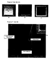
- Figure 7 shows a) scanning electron microscope (SEM) image of an anchor of a thin film wafer level package according to this disclosure, after 60' VHF release of the MEM device.
- the anchor is configured as a grid of cavities within the anchor frame. It is clear that the SiO 2 in the cavities has been removed in the outer anchor lane. The SiO 2 in the middle part has been attacked by the release fluid, while the inner part is still intact; (b) Representation of the VHF attack of SiO 2 in the cavities of the anchor of (a). The oxide is shown in white while the SiGe anchor frame is shown in grey. In the outer part of the anchor the oxide is removed (dark color).
- Figure 8 shows shear force results from thin film wafer level packages, according to this disclosure, with 20 nm soft sputter etch (SSE) and Ti-TiN interlayer (diamond) compared to results from the standard process (square) and the MIL-standard (sloped line). Samples were released using a 60' VHF release process. The indicated thickness removed during the Ar SSE step, is equivalent to the thickness removed with this process for SiO 2 on blanket wafers.
- SSE soft sputter etch
- Ti-TiN interlayer diamond
- FIG 9 shows anchor designs, according to this disclosure, that do not meet the MIL-standard specifications.
- the anchor is configured as an array of concentric SiGe polygons whereby the space between the different polygons is filled with SiO2.
- These anchor designs correspond to the dots on Figure 8 falling below the sloped line (MIL) indicative of the MIL reference.
- Figure 10 shows a SEM picture of anchor (c) from Figure 9 . It can be seen that the VHF released fluid has attacked the SiO 2 inside the anchor.
- Figure 11 shows the shear force of strongest anchor designs, i.e. the cavities are arranged as a grid, according to this disclosure, after 60' VHF release (diamond) and a comparison with standard (triangle) release process.
- the MIL reference line (MIL) is also added. For each measurement point the corresponding anchor structure is shown on top of the figure.
- Figure 12 shows the shear force results for different anchor designs, according to this disclosure, with varying number of anchor lanes for SSE samples released with VHF (diamond) and for samples released with BHF (square).
- the MIL reference line (MIL) is also added. For each measurement point the corresponding anchor structure is shown on top of the figure.
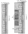
- Figures 13 to 18 illustrate by means of schematic cross sections a process flow according to this disclosure.
- top, bottom, over, under and the like in the description and the claims are used for descriptive purposes and not necessarily for describing relative positions. The terms so used are interchangeable under appropriate circumstances and the embodiments of the disclosure described herein can operate in other orientations than described or illustrated herein.
- a thin film wafer level package comprising a membrane supported by and connected via an anchor frame to a substrate thereby forming a chamber, wherein the anchor frame comprises at least one cavity.
- These closed-loop walls can be concentric. These closed-loop walls preferably have the same width.
- the cavity between the closed-loop walls can be formed by the spacing between these closed-loop walls or can be configured as a grid of cavities, whereby the closed-loop walls are interconnected.
- the membrane and the anchor frame can be formed of the same material.
- this material is silicon-germanium.
- the cavity in the anchor frame can be filled, preferably with silicon-oxide.
- a microelectronic device comprising a thin film wafer level package according to the first aspect.
- This microelectronic device can further comprise a MEM device contained in the chamber of the thin film wafer level package.
- a method for forming a thin film wafer level package on a substrate comprises forming a sacrificial layer on the substrate, forming at least two closed-loop trenches through this sacrificial layer, forming a layer filling these closed-loop trenches thereby defining a cavity between each pair of closed-loop trenches, the cavity being filled with the material of the sacrificial layer, and forming a layer overlying the closed-loop trenches and the area between the closed-loop trenches.
- the step of forming at least two closed-loop trenches can further comprise forming at least one trench connecting these closed-loop trenches.
- the overlying layer will constitute the membrane of the thin film wafer level package while the filling material is part of the anchor frame thereof.
- the filling layer and the overlying layer are formed simultaneously.
- silicon-germanium is used to form the filling and overlying layer.
- the material of the sacrificial layer is silicon oxide.
- the thin film wafer packages in this disclosure were manufactured using SiGe as structural material to form the membrane overlying the chamber containing the MEM device and the anchors supporting the membrane and connecting it to the substrate.
- SiGe SiGe
- Using SiGe to form the thin film wafer level package as well as the encapsulated MEM device has advantages from integration point of view.
- the present disclosure is not limited to SiGe packages.
- Other materials can be used to form the thin film wafer level package and the materials used need not be the same as the materials used to form the MEM device.
- Figure 1 shows a schematic cross-section of a thin film wafer level package, according to this disclosure, before removal of the sacrificial layer within the chamber encapsulated by the thin film wafer level package.
- the membrane overlying the sacrificial layer of the chamber release or etch holes 14 are present to this purpose.
- the thin film wafer level package of figure 1 was realized using SiGe, preferably poly-SiGe, as membrane layer.
- the test structure of figure 1 was formed on a semiconductor, e.g. Si, substrate.
- the test structure is configured as closed chamber, here a poly-SiGe bordered chamber, on top of a protective layer, here a 400 nm SiC layer (deposited as 4 x 100 nm).
- This SiC layer acts as a CMOS protection layer in case these CMOS-compatible packages are built on top of CMOS, i.e. on top of a substrate containing electronic circuitry typically formed using CMOS process technology. In normal operation this chamber contains the MEM device to be packaged.
- this protective layer here SiC, a 400 nm thick SiGe layer is deposited and patterned to remain at the location of the anchors of the thin film package.
- this SiGe layer is also used to form the lower electrode layer of the MEM device.
- a sacrificial layer here a 3 ⁇ m thick High Density Plasma (HDP) SiO 2 , is deposited which was used as a sacrificial layer.
- HDP High Density Plasma
- the MEM device is embedded in this sacrificial layer.
- Closed-looped trenches are etched throughout this sacrificial layer thereby stopping on the underlying patterned poly-SiGe layer. These trenches encircle the area of the chamber, which in normal operation contains the MEM device. Between each pair of trenches the material of the sacrificial layer remained thereby forming spacing between these trenches. The layout of these trenches is discussed in more detail in paragraphs below.
- trenches are filled during the deposition of the material of the membrane layer; here 4 ⁇ m thick poly-SiGe has been deposited.
- the filled trenches now define a cavity which is filled with the remaining material of the sacrificial layer. Only one value for trench width of small width, e.g. 1 ⁇ m, is used for all trenches to ensure a planarised membrane layer after deposition of the poly-SiGe membrane layer.
- the width of the trench is chosen to have minimal or no impact on the planarity of the subsequently formed membrane layer. Additional trenches can be formed to increase the overall area of the anchor frame if needed.
- the membrane layer is patterned to define the thin film packages formed on the single substrate. During this patterning step there is also the definition of the etch holes, that are needed to remove the sacrificial layer from the chamber inside the package.
- Figures 2 (a) and (b) shows examples of different anchor designs for a thin film wafer level package according to this disclosure: (a) the cavities in the anchor, here SiGe, frame are formed as continuous lines, (b) the cavities in the anchor, here, SiGe, frame are formed as a grid of, optionally interconnected, cavities.
- the grey lines are the poly-SiGe walls of the SiGe frame, while the white color represents the cavities within this SiGe frame which are filled with the sacrificial material, here SiO 2 .
- Anchor designs are thus a combination of at least two concentric trench rings, preferably of equal width, with and without connections and with different spacing.
- the sacrificial layer of the chamber is removed through etch or release holes in the membrane layer.
- BHF wet buffered HF
- VHF dry vapor HF
- the inner size of the packages was 100 x 100 ⁇ m 2 .
- the anchor width varies from 1 to 20 ⁇ m.
- Shear tests were done using a Condor 250 tool from XYZTEC.
- a 100 ⁇ m wide needle moves horizontally over the surface comprising the released packages.
- the test structures were placed in rows of 10.
- the tool registers the force needed to move the needle.
- An example of such a measurement is shown in figure 3 . Every peak in this graph corresponds to a position where the needle touches a package. A higher peak corresponds to a stronger package.
- Figure 4 shows the shear force obtained for different anchor designs released with either BHF (dark triangle) or VHF (grey start) together with the minimum shear force specified by the MIL-STD 883E standard (method 2019.5).
- BHF dark triangle
- VHF grey start
- the BHF released samples all met the required standard, as the corresponding points are above the MIL reference line, while not all VHF samples reached this MIL spec.
- the failing mechanisms for both BHF and VHF released samples can be derived from the pictures shown in figures 5 (a) and (b) .
- the BHF released samples it can be seen in figure 5b that the underlying SiC protective layer delaminated during the release process. This means that the anchors themselves are even stronger than the value plotted in figure 4 .
- delaminating occurred between the thin poly-SiGe frame and the 4 ⁇ m thick poly-SiGe membrane as the thin poly-SiGe frame is still visible in figure 5c .
- the interface between the anchors and the membrane was the weakest interface and the results of these samples were therefore used to study the effect of the anchor design on the mechanical strength of the package.
- Figure 6 shows the shear force for VHF released samples with increasing anchor width, i.e. increasing number of SiGe anchor lanes as each anchor lane had the same width defined by the patterning of the trenches in the sacrificial layer. It can be seen that the shear force increases with number of anchor lines. There is a monotonous linear behavior between the samples having 1 to 3 SiGe anchor lanes. For samples having anchors with 4 or 5 lanes there is an upward shift of the shear force.
- the offset between anchor frame with different number of anchor lanes, here SiGe walls, can be explained by the attack of the SiO 2 incorporated in the anchor frame as further discussed below.
- FIG. 7 shows a) scanning electron microscope (SEM) image of an anchor of a thin film wafer level package according to this disclosure, after 60' VHF release of the MEM device.
- the anchor is configured as a grid of cavities within the anchor frame. It is clear that the SiO 2 in the cavities has been removed in the outer anchor lane. The SiO 2 in the middle part has been attacked by the release fluid, while the inner part is still intact; (b) Representation of the VHF attack of SiO 2 in the cavities of the anchor of (a).
- the oxide is shown in white while the SiGe anchor frame is shown in grey. In the outer part of the anchor the oxide is removed (dark color).
- the contact area between the anchor and the substrate is reduced and therefore the force needed to destroy the package is also reduced.
- substantially all SiO 2 is assumed to be gone in the anchor region, while some SiO 2 is probably remaining for anchors with more lanes.
- the extent to which the cavity filing material is removed from the anchor frame during the release process will depend on the material used to form the anchor frame, the dimensions of the frame in particular the width of the anchor lanes defined by the trenches etched in the sacrificial material, the sacrificial material used and the release process itself.
- New samples were prepared with the use of an Ar soft sputter etch (SSE) and the deposition of a Ti-TiN (5-10 nm) interlayer on the sacrificial layer before the deposition of the membrane layer, here poly-SiGe.
- SSE Ar soft sputter etch
- Ti-TiN 5-10 nm
- the soft sputter etch removed the native oxide present on exposed surfaces of the thin poly-SiGe anchor frame.
- the Ti-TiN interlayer helped in reducing the impact of the remaining native oxides. These native oxides can form a path for the VHF release fluid to attack the SiO 2 inside the anchors. Removal of the native oxides enhanced the VHF compatibility of the anchors.
- a Ti-TiN interlayer improved the adhesion between the thin SiGe anchor frame and the SiGe membrane layer.
- Figure 8 shows the shear force required for the different anchor designs after a 60' VHF release process on test samples prepared with the manufacturing process without (standard: grey square) and with (SSE+Ti_TiN: dark diamond) a soft sputter etch, here with 20 nm SSE, and an interlayer, here a Ti-TiN interlayer. Also the MIL-standard is shown as reference. As can be seen in figure 8, for most anchor designs the anchor strength is largely improved when using the manufacturing process with soft sputter etch and interface layer. About 85% of all anchor designs now met the MIL specification.
- Figure 9 shows anchor designs of samples with SSE and Ti-TiN interlayer that did not meet the MIL-standard.
- the SiO 2 to SiGe membrane contact area was larger for these anchor layouts than the SiGe to SiGe membrane contact area. This indicates that for samples with a Ti-TiN interlayer the anchor strength is mainly coming from the SiGe to SiGe interface.
- each anchor design for which the ratio [SiGe-SiGe anchor area/ SiO 2 -SiGe anchor area] was larger than 1 reached the MIL-standard.
- the anchor is less prone to the release process and will have a higher shear force. This increased mechanical strength is believed to be a consequence of the improved adhesion between the two SiGe layers, i.e. anchor frame and membrane layer, in the anchor region.
- Figure 11 depicts the strongest anchor designs for samples manufactured with and without the SSE and Ti-TiN interlayer. From all tested anchor design, these designs had the largest SiGe-SiGe anchor area in line with the conclusion drawn above. This increased contact area was obtained by layouting the anchor frame as a grid of SiGe walls whereby the gaps between these walls are filled with oxide.
- Figure 12 shows the shear force results for different anchor designs, according to this disclosure, with varying number of anchor lanes for SSE samples released with VHF (diamond) and for samples released with BHF (square).
- the MIL reference line (MIL) is also added. For each measurement point the corresponding anchor structure is shown on top of the figure.
- Figures 13 to 18 schematically illustrate a process flow for manufacturing packaged MEM devices according to this disclosure.
- Figure 13 shows a substrate 1, for instance a silicon wafer.
- a silicon oxide (SiO 2 ) layer 2 with a thickness of e.g. 300 nm, is deposited.
- a patterned conductive layer comprising different sub layers 3 is formed on top of the layer 2.
- the sub layers can comprise for instance a Ti/AlCu/Ti/TiN stack with a thickness of for instance 20 nm/590 nm/20 nm/45 nm.
- the substrate 1 is a CMOS substrate
- the metal layer 3 can be the top metal layer of an interconnect scheme of this semiconductor substrate comprising active components such as circuits.
- the MEMS device is then processed on top of electronic circuitry formed on this substrate.
- a silicon oxide (SiO 2 ) layer 4 of about 1500 nm thickness is deposited.
- a 300 to 400 nm SiC protection layer 5 is deposited on the oxide layer 4. Openings in layers 5 and 4 are present to form contact holes to the metal layer 3. Via the contact holes an electrical connection can be formed between on the one hand a MEMS device in the cavity and on the other hand the bond pad adjacent to the cavity.
- a silicon germanium electrode layer 6 is deposited by means of chemical vapour deposition (CVD), for instance having a thickness of 400 nm, and being connected to the top CMOS electrode layer 3.
- the silicon germanium layer 6 is patterned into silicon germanium electrodes as shown in figure 14 .
- This patterned SiGe layer 6 also contains the area 73 where the anchor frame is to be formed.
- Another sacrificial silicon oxide (SiO 2 ) layer 7 (thickness typically of about 1 to 3 ⁇ m) is deposited.
- the sacrificial layer is planarized by applying a chemical mechanical polishing step, reducing the surface topography for the further lithography steps.
- a further contact etch is performed by opening the sacrificial oxide 7 to define packaging anchors 72, MEMS feed-throughs 73 and the contact 71 to the MEM device as shown in figure 15 .
- the structural silicon germanium layer 8 is deposited typically with a thickness of 1 to 8 ⁇ m, optionally together with a 100 nm SiC layer 9 (not depicted).
- the structural layer is used to form the MEMS device and the anchor of the thin film packages.
- the structural silicon germanium layer (and optionally the SiC layer) is patterned to form the MEMS device 84, part of the packaging anchors 82 and part of the electrical connection 83 between the buried metal layer 3 and the bond pad.
- the patterning of the packaging anchors 82 is done according to the layout considerations above. In the process flow illustrated by figures 13 to 18 the anchor is shown as a single SiGe anchor lane.
- the structure is covered by depositing a sacrificial silicon oxide layer 10 filling the gaps within the structural layer including the spacing between the SiGe anchor walls as shown in figure 16 .
- the membrane contact etch is performed in the oxide layer 10, to form the anchors 82 of the capping layer and part of the electric connection 81 to the bond pad.
- the patterning of the oxide layer 10 with respect to the anchors 82 is done according to the layout considerations above.
- remaining portions 101 of the sacrificial layer are present, which can support the electrical connection 81 and the package sidewall or cavity sidewall.
- the remaining portion has a substantially flat upper surface.
- the polycrystalline silicon germanium membrane 12 deposition is performed (typically having a thickness of 4-10 ⁇ m), to obtain substantially flat silicon germanium membrane.
- the level of the substantially flat upper surface of the remaining portion of sacrificial material 101 corresponds to the level of the lower surface the membrane layer 12.
- the etch hole definition is performed to define the release holes 14 which will be used for removing the sacrificial material 10 under the membrane layer 12 as shown in figure 17 . As explained above these release holes cannot be formed within anchor area.
- the release of the membrane layer and of the functional silicon germanium layer within the formed cavity can be performed by using an etching agent, for instance HF in the gas phase, which is passing through the openings or release holes 14 in the membrane layer 12, in order to remove the material of the sacrificial layers 10 (optionally 11), 7, hereby creating cavity (chamber) or gap 15 below the membrane layer 12, the cavity comprising the MEMS device as shown in figure 18 .
- an etching agent for instance HF in the gas phase
- Further processing of the packaged MEM device can be done using known manufacturing techniques to provide e.g. sealing of the release holes 14, forming the electrical connection to the MEM bonding pads and dicing of the individual packaged MEM devices.
Landscapes
- Engineering & Computer Science (AREA)
- Microelectronics & Electronic Packaging (AREA)
- Computer Hardware Design (AREA)
- Micromachines (AREA)
- Physical Vapour Deposition (AREA)
Applications Claiming Priority (1)
| Application Number | Priority Date | Filing Date | Title |
|---|---|---|---|
| US29738610P | 2010-01-22 | 2010-01-22 |
Publications (3)
| Publication Number | Publication Date |
|---|---|
| EP2365521A2 true EP2365521A2 (fr) | 2011-09-14 |
| EP2365521A3 EP2365521A3 (fr) | 2014-06-04 |
| EP2365521B1 EP2365521B1 (fr) | 2018-12-26 |
Family
ID=44262903
Family Applications (1)
| Application Number | Title | Priority Date | Filing Date |
|---|---|---|---|
| EP11075009.8A Not-in-force EP2365521B1 (fr) | 2010-01-22 | 2011-01-20 | Encapsulation sur tranche à couche mince |
Country Status (3)
| Country | Link |
|---|---|
| US (1) | US8592998B2 (fr) |
| EP (1) | EP2365521B1 (fr) |
| JP (1) | JP5779355B2 (fr) |
Families Citing this family (9)
| Publication number | Priority date | Publication date | Assignee | Title |
|---|---|---|---|---|
| US8368153B2 (en) * | 2010-04-08 | 2013-02-05 | United Microelectronics Corp. | Wafer level package of MEMS microphone and manufacturing method thereof |
| DE102012210049A1 (de) * | 2012-06-14 | 2013-12-19 | Robert Bosch Gmbh | Hybrid integriertes Bauteil und Verfahren zu dessen Herstellung |
| US9630834B2 (en) * | 2014-06-16 | 2017-04-25 | InSense, Inc. | Wafer scale monolithic CMOS-integration of free- and non-free-standing Metal- and Metal alloy-based MEMS structures in a sealed cavity |
| US9458010B1 (en) | 2015-07-22 | 2016-10-04 | Freescale Semiconductor, Inc. | Systems and methods for anchoring components in MEMS semiconductor devices |
| US10329142B2 (en) * | 2015-12-18 | 2019-06-25 | Samsung Electro-Mechanics Co., Ltd. | Wafer level package and method of manufacturing the same |
| CN105621341A (zh) * | 2015-12-29 | 2016-06-01 | 苏州工业园区纳米产业技术研究院有限公司 | 一种mems锚区结构及其制备方法 |
| JP6461030B2 (ja) | 2016-03-15 | 2019-01-30 | 株式会社東芝 | 電子装置及び電子装置の製造方法 |
| JP6472469B2 (ja) * | 2017-02-15 | 2019-02-20 | Sppテクノロジーズ株式会社 | SiGe層のエッチング方法 |
| CN108298495B (zh) * | 2017-12-19 | 2020-10-16 | 烟台艾睿光电科技有限公司 | 一种金属锚点填充工艺以及热探测器件 |
Family Cites Families (11)
| Publication number | Priority date | Publication date | Assignee | Title |
|---|---|---|---|---|
| CA2176052A1 (fr) * | 1995-06-07 | 1996-12-08 | James D. Seefeldt | Transducteur a faisceau resonnant au silicium et methode correspondante |
| DE10006035A1 (de) * | 2000-02-10 | 2001-08-16 | Bosch Gmbh Robert | Verfahren zur Herstellung eines mikromechanischen Bauelements sowie ein nach dem Verfahren hergestelltes Bauelement |
| US6465280B1 (en) * | 2001-03-07 | 2002-10-15 | Analog Devices, Inc. | In-situ cap and method of fabricating same for an integrated circuit device |
| US6635506B2 (en) * | 2001-11-07 | 2003-10-21 | International Business Machines Corporation | Method of fabricating micro-electromechanical switches on CMOS compatible substrates |
| EP1843971B1 (fr) * | 2005-02-04 | 2016-04-13 | Imec | Procede d'encapsulation d'un dispositif dans une microcavite |
| US7358106B2 (en) * | 2005-03-03 | 2008-04-15 | Stellar Micro Devices | Hermetic MEMS package and method of manufacture |
| FR2901264B1 (fr) * | 2006-05-22 | 2008-10-10 | Commissariat Energie Atomique | Microcomposant muni d'une cavite delimitee par un capot a resistance mecanique amelioree |
| EP1908727A1 (fr) * | 2006-10-03 | 2008-04-09 | Seiko Epson Corporation | Boîtier pour MEMS au niveau de plaquette et sa méthode de fabrication |
| US20080090320A1 (en) * | 2006-10-17 | 2008-04-17 | John Heck | Self sealed MEMS device |
| KR100995541B1 (ko) * | 2008-03-26 | 2010-11-22 | 한국과학기술원 | 마이크로 전자기계 시스템 소자의 패키징 방법 및 그패키지 |
| EP2327658B1 (fr) * | 2009-11-30 | 2018-07-04 | IMEC vzw | Procédé de fabrication de dispositifs microélectroniques et dispositifs correspondants |
-
2011
- 2011-01-20 EP EP11075009.8A patent/EP2365521B1/fr not_active Not-in-force
- 2011-01-21 JP JP2011011013A patent/JP5779355B2/ja not_active Expired - Fee Related
- 2011-01-24 US US13/012,275 patent/US8592998B2/en not_active Expired - Fee Related
Non-Patent Citations (1)
| Title |
|---|
| None |
Also Published As
| Publication number | Publication date |
|---|---|
| US20110180943A1 (en) | 2011-07-28 |
| US8592998B2 (en) | 2013-11-26 |
| EP2365521A3 (fr) | 2014-06-04 |
| JP2011152636A (ja) | 2011-08-11 |
| JP5779355B2 (ja) | 2015-09-16 |
| EP2365521B1 (fr) | 2018-12-26 |
Similar Documents
| Publication | Publication Date | Title |
|---|---|---|
| US8592998B2 (en) | Thin film wafer level package | |
| US10155659B2 (en) | Vacuum sealed MEMS and CMOS package | |
| US8709849B2 (en) | Wafer level packaging | |
| KR100833508B1 (ko) | 멤즈 패키지 및 그 방법 | |
| US20120256308A1 (en) | Method for Sealing a Micro-Cavity | |
| US9991340B2 (en) | Mechanical stress-decoupling in semiconductor device | |
| US20080054759A1 (en) | Wafer-level encapsulation and sealing of electrostatic transducers | |
| US20220348455A1 (en) | Systems and methods for providing getters in microelectromechanical systems | |
| TWI624954B (zh) | 在單一晶片上的慣性和壓力感測器 | |
| WO2012142368A1 (fr) | Électrode hors plan délimitée par une entretoise | |
| JP5911194B2 (ja) | マイクロエレクトロニクスデバイスの製造方法およびその方法によるデバイス | |
| TW202308935A (zh) | 用於製造微機電系統裝置的方法及系統 | |
| EP1734001B1 (fr) | Procédé pour encapsuler des MEMS au niveau plaquette | |
| EP2402284A1 (fr) | Procédé de fabrication MEMS | |
| WO2009133506A2 (fr) | Dispositif de système micro-électromécanique et procédé de fabrication | |
| US20070298532A1 (en) | Micro-Electro-mechanical (MEMS) encapsulation using buried porous silicon | |
| US20050079684A1 (en) | Method of manufacturing an accelerometer | |
| TW201447992A (zh) | 用於面外間隔體界定電極的磊晶式多晶矽蝕刻停止 | |
| CN120752195A (zh) | 用于制造半导体构件的方法和微镜组件 | |
| Messana et al. | Packaging of large lateral deflection MEMS using a combination of fusion bonding and epitaxial reactor sealing | |
| Rajaraman et al. | Robust wafer-level thin-film encapsulation of microstructures using low stress PECVD silicon carbide | |
| US7531424B1 (en) | Vacuum wafer-level packaging for SOI-MEMS devices | |
| Claes et al. | Influence of the novel anchor design on the shear strength of poly-SiGe thin film wafer level packages | |
| TWI427714B (zh) | 一種半導體組件與形成密封環的方法 |
Legal Events
| Date | Code | Title | Description |
|---|---|---|---|
| PUAI | Public reference made under article 153(3) epc to a published international application that has entered the european phase |
Free format text: ORIGINAL CODE: 0009012 |
|
| AK | Designated contracting states |
Kind code of ref document: A2 Designated state(s): AL AT BE BG CH CY CZ DE DK EE ES FI FR GB GR HR HU IE IS IT LI LT LU LV MC MK MT NL NO PL PT RO RS SE SI SK SM TR |
|
| AX | Request for extension of the european patent |
Extension state: BA ME |
|
| PUAL | Search report despatched |
Free format text: ORIGINAL CODE: 0009013 |
|
| AK | Designated contracting states |
Kind code of ref document: A3 Designated state(s): AL AT BE BG CH CY CZ DE DK EE ES FI FR GB GR HR HU IE IS IT LI LT LU LV MC MK MT NL NO PL PT RO RS SE SI SK SM TR |
|
| AX | Request for extension of the european patent |
Extension state: BA ME |
|
| RIC1 | Information provided on ipc code assigned before grant |
Ipc: B81B 7/00 20060101AFI20140425BHEP |
|
| 17P | Request for examination filed |
Effective date: 20141121 |
|
| RBV | Designated contracting states (corrected) |
Designated state(s): AL AT BE BG CH CY CZ DE DK EE ES FI FR GB GR HR HU IE IS IT LI LT LU LV MC MK MT NL NO PL PT RO RS SE SI SK SM TR |
|
| STAA | Information on the status of an ep patent application or granted ep patent |
Free format text: STATUS: EXAMINATION IS IN PROGRESS |
|
| 17Q | First examination report despatched |
Effective date: 20170703 |
|
| RAP1 | Party data changed (applicant data changed or rights of an application transferred) |
Owner name: KATHOLIEKE UNIVERSITEIT LEUVEN, K.U. LEUVEN R&D Owner name: IMEC VZW |
|
| GRAP | Despatch of communication of intention to grant a patent |
Free format text: ORIGINAL CODE: EPIDOSNIGR1 |
|
| STAA | Information on the status of an ep patent application or granted ep patent |
Free format text: STATUS: GRANT OF PATENT IS INTENDED |
|
| INTG | Intention to grant announced |
Effective date: 20180712 |
|
| GRAS | Grant fee paid |
Free format text: ORIGINAL CODE: EPIDOSNIGR3 |
|
| GRAA | (expected) grant |
Free format text: ORIGINAL CODE: 0009210 |
|
| STAA | Information on the status of an ep patent application or granted ep patent |
Free format text: STATUS: THE PATENT HAS BEEN GRANTED |
|
| AK | Designated contracting states |
Kind code of ref document: B1 Designated state(s): AL AT BE BG CH CY CZ DE DK EE ES FI FR GB GR HR HU IE IS IT LI LT LU LV MC MK MT NL NO PL PT RO RS SE SI SK SM TR |
|
| REG | Reference to a national code |
Ref country code: GB Ref legal event code: FG4D |
|
| REG | Reference to a national code |
Ref country code: CH Ref legal event code: EP |
|
| REG | Reference to a national code |
Ref country code: AT Ref legal event code: REF Ref document number: 1081141 Country of ref document: AT Kind code of ref document: T Effective date: 20190115 |
|
| REG | Reference to a national code |
Ref country code: DE Ref legal event code: R096 Ref document number: 602011055051 Country of ref document: DE |
|
| REG | Reference to a national code |
Ref country code: IE Ref legal event code: FG4D |
|
| PG25 | Lapsed in a contracting state [announced via postgrant information from national office to epo] |
Ref country code: LT Free format text: LAPSE BECAUSE OF FAILURE TO SUBMIT A TRANSLATION OF THE DESCRIPTION OR TO PAY THE FEE WITHIN THE PRESCRIBED TIME-LIMIT Effective date: 20181226 Ref country code: NO Free format text: LAPSE BECAUSE OF FAILURE TO SUBMIT A TRANSLATION OF THE DESCRIPTION OR TO PAY THE FEE WITHIN THE PRESCRIBED TIME-LIMIT Effective date: 20190326 Ref country code: FI Free format text: LAPSE BECAUSE OF FAILURE TO SUBMIT A TRANSLATION OF THE DESCRIPTION OR TO PAY THE FEE WITHIN THE PRESCRIBED TIME-LIMIT Effective date: 20181226 Ref country code: BG Free format text: LAPSE BECAUSE OF FAILURE TO SUBMIT A TRANSLATION OF THE DESCRIPTION OR TO PAY THE FEE WITHIN THE PRESCRIBED TIME-LIMIT Effective date: 20190326 Ref country code: HR Free format text: LAPSE BECAUSE OF FAILURE TO SUBMIT A TRANSLATION OF THE DESCRIPTION OR TO PAY THE FEE WITHIN THE PRESCRIBED TIME-LIMIT Effective date: 20181226 Ref country code: LV Free format text: LAPSE BECAUSE OF FAILURE TO SUBMIT A TRANSLATION OF THE DESCRIPTION OR TO PAY THE FEE WITHIN THE PRESCRIBED TIME-LIMIT Effective date: 20181226 |
|
| REG | Reference to a national code |
Ref country code: NL Ref legal event code: MP Effective date: 20181226 |
|
| REG | Reference to a national code |
Ref country code: LT Ref legal event code: MG4D |
|
| PG25 | Lapsed in a contracting state [announced via postgrant information from national office to epo] |
Ref country code: RS Free format text: LAPSE BECAUSE OF FAILURE TO SUBMIT A TRANSLATION OF THE DESCRIPTION OR TO PAY THE FEE WITHIN THE PRESCRIBED TIME-LIMIT Effective date: 20181226 Ref country code: SE Free format text: LAPSE BECAUSE OF FAILURE TO SUBMIT A TRANSLATION OF THE DESCRIPTION OR TO PAY THE FEE WITHIN THE PRESCRIBED TIME-LIMIT Effective date: 20181226 Ref country code: AL Free format text: LAPSE BECAUSE OF FAILURE TO SUBMIT A TRANSLATION OF THE DESCRIPTION OR TO PAY THE FEE WITHIN THE PRESCRIBED TIME-LIMIT Effective date: 20181226 Ref country code: GR Free format text: LAPSE BECAUSE OF FAILURE TO SUBMIT A TRANSLATION OF THE DESCRIPTION OR TO PAY THE FEE WITHIN THE PRESCRIBED TIME-LIMIT Effective date: 20190327 |
|
| REG | Reference to a national code |
Ref country code: AT Ref legal event code: MK05 Ref document number: 1081141 Country of ref document: AT Kind code of ref document: T Effective date: 20181226 |
|
| PG25 | Lapsed in a contracting state [announced via postgrant information from national office to epo] |
Ref country code: NL Free format text: LAPSE BECAUSE OF FAILURE TO SUBMIT A TRANSLATION OF THE DESCRIPTION OR TO PAY THE FEE WITHIN THE PRESCRIBED TIME-LIMIT Effective date: 20181226 |
|
| PG25 | Lapsed in a contracting state [announced via postgrant information from national office to epo] |
Ref country code: ES Free format text: LAPSE BECAUSE OF FAILURE TO SUBMIT A TRANSLATION OF THE DESCRIPTION OR TO PAY THE FEE WITHIN THE PRESCRIBED TIME-LIMIT Effective date: 20181226 Ref country code: PL Free format text: LAPSE BECAUSE OF FAILURE TO SUBMIT A TRANSLATION OF THE DESCRIPTION OR TO PAY THE FEE WITHIN THE PRESCRIBED TIME-LIMIT Effective date: 20181226 Ref country code: IT Free format text: LAPSE BECAUSE OF FAILURE TO SUBMIT A TRANSLATION OF THE DESCRIPTION OR TO PAY THE FEE WITHIN THE PRESCRIBED TIME-LIMIT Effective date: 20181226 Ref country code: PT Free format text: LAPSE BECAUSE OF FAILURE TO SUBMIT A TRANSLATION OF THE DESCRIPTION OR TO PAY THE FEE WITHIN THE PRESCRIBED TIME-LIMIT Effective date: 20190426 Ref country code: CZ Free format text: LAPSE BECAUSE OF FAILURE TO SUBMIT A TRANSLATION OF THE DESCRIPTION OR TO PAY THE FEE WITHIN THE PRESCRIBED TIME-LIMIT Effective date: 20181226 |
|
| PG25 | Lapsed in a contracting state [announced via postgrant information from national office to epo] |
Ref country code: SM Free format text: LAPSE BECAUSE OF FAILURE TO SUBMIT A TRANSLATION OF THE DESCRIPTION OR TO PAY THE FEE WITHIN THE PRESCRIBED TIME-LIMIT Effective date: 20181226 Ref country code: IS Free format text: LAPSE BECAUSE OF FAILURE TO SUBMIT A TRANSLATION OF THE DESCRIPTION OR TO PAY THE FEE WITHIN THE PRESCRIBED TIME-LIMIT Effective date: 20190426 Ref country code: RO Free format text: LAPSE BECAUSE OF FAILURE TO SUBMIT A TRANSLATION OF THE DESCRIPTION OR TO PAY THE FEE WITHIN THE PRESCRIBED TIME-LIMIT Effective date: 20181226 Ref country code: EE Free format text: LAPSE BECAUSE OF FAILURE TO SUBMIT A TRANSLATION OF THE DESCRIPTION OR TO PAY THE FEE WITHIN THE PRESCRIBED TIME-LIMIT Effective date: 20181226 Ref country code: SK Free format text: LAPSE BECAUSE OF FAILURE TO SUBMIT A TRANSLATION OF THE DESCRIPTION OR TO PAY THE FEE WITHIN THE PRESCRIBED TIME-LIMIT Effective date: 20181226 |
|
| REG | Reference to a national code |
Ref country code: CH Ref legal event code: PL |
|
| REG | Reference to a national code |
Ref country code: DE Ref legal event code: R097 Ref document number: 602011055051 Country of ref document: DE |
|
| PG25 | Lapsed in a contracting state [announced via postgrant information from national office to epo] |
Ref country code: LU Free format text: LAPSE BECAUSE OF NON-PAYMENT OF DUE FEES Effective date: 20190120 |
|
| REG | Reference to a national code |
Ref country code: BE Ref legal event code: MM Effective date: 20190131 |
|
| REG | Reference to a national code |
Ref country code: IE Ref legal event code: MM4A |
|
| PG25 | Lapsed in a contracting state [announced via postgrant information from national office to epo] |
Ref country code: DK Free format text: LAPSE BECAUSE OF FAILURE TO SUBMIT A TRANSLATION OF THE DESCRIPTION OR TO PAY THE FEE WITHIN THE PRESCRIBED TIME-LIMIT Effective date: 20181226 Ref country code: AT Free format text: LAPSE BECAUSE OF FAILURE TO SUBMIT A TRANSLATION OF THE DESCRIPTION OR TO PAY THE FEE WITHIN THE PRESCRIBED TIME-LIMIT Effective date: 20181226 Ref country code: MC Free format text: LAPSE BECAUSE OF FAILURE TO SUBMIT A TRANSLATION OF THE DESCRIPTION OR TO PAY THE FEE WITHIN THE PRESCRIBED TIME-LIMIT Effective date: 20181226 |
|
| PLBE | No opposition filed within time limit |
Free format text: ORIGINAL CODE: 0009261 |
|
| STAA | Information on the status of an ep patent application or granted ep patent |
Free format text: STATUS: NO OPPOSITION FILED WITHIN TIME LIMIT |
|
| GBPC | Gb: european patent ceased through non-payment of renewal fee |
Effective date: 20190326 |
|
| PG25 | Lapsed in a contracting state [announced via postgrant information from national office to epo] |
Ref country code: BE Free format text: LAPSE BECAUSE OF NON-PAYMENT OF DUE FEES Effective date: 20190131 |
|
| 26N | No opposition filed |
Effective date: 20190927 |
|
| PG25 | Lapsed in a contracting state [announced via postgrant information from national office to epo] |
Ref country code: LI Free format text: LAPSE BECAUSE OF NON-PAYMENT OF DUE FEES Effective date: 20190131 Ref country code: CH Free format text: LAPSE BECAUSE OF NON-PAYMENT OF DUE FEES Effective date: 20190131 |
|
| PG25 | Lapsed in a contracting state [announced via postgrant information from national office to epo] |
Ref country code: IE Free format text: LAPSE BECAUSE OF NON-PAYMENT OF DUE FEES Effective date: 20190120 Ref country code: GB Free format text: LAPSE BECAUSE OF NON-PAYMENT OF DUE FEES Effective date: 20190326 |
|
| PG25 | Lapsed in a contracting state [announced via postgrant information from national office to epo] |
Ref country code: SI Free format text: LAPSE BECAUSE OF FAILURE TO SUBMIT A TRANSLATION OF THE DESCRIPTION OR TO PAY THE FEE WITHIN THE PRESCRIBED TIME-LIMIT Effective date: 20181226 |
|
| PG25 | Lapsed in a contracting state [announced via postgrant information from national office to epo] |
Ref country code: TR Free format text: LAPSE BECAUSE OF FAILURE TO SUBMIT A TRANSLATION OF THE DESCRIPTION OR TO PAY THE FEE WITHIN THE PRESCRIBED TIME-LIMIT Effective date: 20181226 |
|
| PG25 | Lapsed in a contracting state [announced via postgrant information from national office to epo] |
Ref country code: MT Free format text: LAPSE BECAUSE OF NON-PAYMENT OF DUE FEES Effective date: 20190120 |
|
| PGFP | Annual fee paid to national office [announced via postgrant information from national office to epo] |
Ref country code: FR Payment date: 20201217 Year of fee payment: 11 |
|
| PG25 | Lapsed in a contracting state [announced via postgrant information from national office to epo] |
Ref country code: CY Free format text: LAPSE BECAUSE OF FAILURE TO SUBMIT A TRANSLATION OF THE DESCRIPTION OR TO PAY THE FEE WITHIN THE PRESCRIBED TIME-LIMIT Effective date: 20181226 |
|
| PGFP | Annual fee paid to national office [announced via postgrant information from national office to epo] |
Ref country code: DE Payment date: 20201217 Year of fee payment: 11 |
|
| PG25 | Lapsed in a contracting state [announced via postgrant information from national office to epo] |
Ref country code: HU Free format text: LAPSE BECAUSE OF FAILURE TO SUBMIT A TRANSLATION OF THE DESCRIPTION OR TO PAY THE FEE WITHIN THE PRESCRIBED TIME-LIMIT; INVALID AB INITIO Effective date: 20110120 |
|
| PG25 | Lapsed in a contracting state [announced via postgrant information from national office to epo] |
Ref country code: MK Free format text: LAPSE BECAUSE OF FAILURE TO SUBMIT A TRANSLATION OF THE DESCRIPTION OR TO PAY THE FEE WITHIN THE PRESCRIBED TIME-LIMIT Effective date: 20181226 |
|
| REG | Reference to a national code |
Ref country code: DE Ref legal event code: R119 Ref document number: 602011055051 Country of ref document: DE |
|
| PG25 | Lapsed in a contracting state [announced via postgrant information from national office to epo] |
Ref country code: DE Free format text: LAPSE BECAUSE OF NON-PAYMENT OF DUE FEES Effective date: 20220802 |
|
| PG25 | Lapsed in a contracting state [announced via postgrant information from national office to epo] |
Ref country code: FR Free format text: LAPSE BECAUSE OF NON-PAYMENT OF DUE FEES Effective date: 20220131 |