EP2365545B1 - Lichtemittierende Vorrichtung, Gehäuse für lichtemittierende Vorrichtung und Beleuchtungssystem - Google Patents
Lichtemittierende Vorrichtung, Gehäuse für lichtemittierende Vorrichtung und Beleuchtungssystem Download PDFInfo
- Publication number
- EP2365545B1 EP2365545B1 EP10193392.7A EP10193392A EP2365545B1 EP 2365545 B1 EP2365545 B1 EP 2365545B1 EP 10193392 A EP10193392 A EP 10193392A EP 2365545 B1 EP2365545 B1 EP 2365545B1
- Authority
- EP
- European Patent Office
- Prior art keywords
- light emitting
- emitting device
- reflective metal
- layer
- metal support
- Prior art date
- Legal status (The legal status is an assumption and is not a legal conclusion. Google has not performed a legal analysis and makes no representation as to the accuracy of the status listed.)
- Not-in-force
Links
Images

Classifications
-
- H—ELECTRICITY
- H10—SEMICONDUCTOR DEVICES; ELECTRIC SOLID-STATE DEVICES NOT OTHERWISE PROVIDED FOR
- H10H—INORGANIC LIGHT-EMITTING SEMICONDUCTOR DEVICES HAVING POTENTIAL BARRIERS
- H10H20/00—Individual inorganic light-emitting semiconductor devices having potential barriers, e.g. light-emitting diodes [LED]
- H10H20/80—Constructional details
- H10H20/83—Electrodes
- H10H20/832—Electrodes characterised by their material
- H10H20/835—Reflective materials
-
- G—PHYSICS
- G02—OPTICS
- G02B—OPTICAL ELEMENTS, SYSTEMS OR APPARATUS
- G02B5/00—Optical elements other than lenses
- G02B5/08—Mirrors
- G02B5/0816—Multilayer mirrors, i.e. having two or more reflecting layers
- G02B5/085—Multilayer mirrors, i.e. having two or more reflecting layers at least one of the reflecting layers comprising metal
- G02B5/0875—Multilayer mirrors, i.e. having two or more reflecting layers at least one of the reflecting layers comprising metal the reflecting layers comprising two or more metallic layers
Definitions
- Embodiments relate to a light emitting device, a light emitting device package, and a lighting system.
- LEDs Light emitting diodes are semiconductor light emitting devices that convert current into light.
- a wavelength of light emitted from such an LED depends on a semiconductor material used for manufacturing the LED. This is done because the wavelength of the emitted light depends on a band-gap of the semiconductor material, which refers to an energy difference between valence band electrons and conduction band electrodes.
- LEDs As brightness of LEDs is gradually increased in recent years, the LEDs are being used as light sources for displays, vehicles, and illuminations. Also, LEDs emitting white light having superior efficiency may be realized by using a fluorescent substance or combining LEDs having various colors.
- Related art is described for example in patent publications WO2009078574A1 , WO0019247A2 , WO2006116030A2 , JPH04213878A and US2009008668A1 .
- Embodiments provide a light emitting device having a new structure, a light emitting device package, and a lighting system.
- Embodiments also provide a light emitting device having improved light efficiency, a light emitting device package, and a lighting system.
- Embodiments also provide a light emitting device having heat radiation efficiency, a light emitting device package, and a lighting system.
- a light emitting device having the above indicated advantages is defined by claim 1. Further advantageous embodiments and the corresponding light emitting device package and a light emitting system are defined in the dependent claims.
- a layer (or film), a region, a pattern, or a structure is referred to as being 'on' a substrate, a layer (or film), a region, a pad, or patterns, it can be directly on another layer or substrate, or intervening layers may also be present. Further, it will be understood that when a layer is referred to as being "under” another layer, it can be directly under another layer, and one or more intervening layers may also be present. Further, the reference about 'on' and 'under' each layer will be made on the basis of drawings.
- each layer is exaggerated, omitted, or schematically illustrated for convenience in description and clarity. Also, the size of each element does not entirely reflect an actual size.
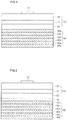
- Fig. 1 is a view of a light emitting device according to a first embodiment that is not part of the invention as claimed.
- a light emitting device includes a reflective metal support 80, a light emitting structure layer 150 on the reflective metal support 80, and an electrode 90 on the light emitting structure layer 150.
- the reflective metal support 80 includes a first reflective metal layer 80a and a second reflective metal layer 80b.
- the first reflective metal layer 80a and the second reflective metal layer 80b are defined as one pair of unit layers, the reflective metal support 80 includes a plurality of pairs of unit layers.
- the reflective metal support 80 includes 2 pairs to 80 pairs of the first and second reflective metal layers 80a and 80b. Particularly, the reflective metal support 80 includes 30 pairs to 70 pairs of the first and second reflective metal layers 80a and 80b, and furthermore, 40 pairs to 60 pairs of the first and second reflective metal layers 80a and 80b are preferred.
- the first reflective metal layer 80a and the second reflective metal layer 80b are formed of different metals.
- each of the first and second reflective metal layers 80a and 80b may have a thickness of about 0.1 ⁇ m to about 10 ⁇ m.
- one of the first and second reflective metal layers 80a and 80b may have a thickness of about 0.4 ⁇ m to about 0.8 ⁇ m
- the other one of the first and second reflective metal layers 80a and 80b may have a thickness of about 0.8 ⁇ m to about 1.2 ⁇ m.
- the reflective metal support 80 includes the plurality of pairs of the first and second reflective metal layers 80a and 80b, which are stacked on each other, and a thickness of about 50 ⁇ m to about 200 ⁇ m.
- the reflective metal support 80 may have a thickness thicker than that of the light emitting structure layer 150.
- the light emitting structure layer 150 may have a thickness of about 3 ⁇ m to about 4 ⁇ m.
- the first reflective metal layer 80a has a compressive stress
- the second reflective metal layer 80b has a tensile stress
- the compressive stress of the first reflective metal layer 80a and the tensile stress of the second reflective metal layer 80b may be offset to each other to reduce a stress of the reflective metal support 80.
- the stress of the reflective metal support 80 since the stress of the reflective metal support 80 has a little effect on the light emitting structure layer 150, the reflective metal support 80 may have a thick thickness.
- the first reflective metal layer 80a may have a compressive stress of about 100 MPa to about 2,000 MPa
- the second reflective metal layer 80b may have a tensile stress of about 100 MPa to about 2,000 MPa.
- the reflective metal support 80 in which the plurality of pairs of the first and second metal layers 80a and 80b, which are stacked on each other, may have a compressive stress or a tensile stress of about 0 MPa to about 2,000 MPa.
- Each of the first and second reflective metal layers 80a and 80b is formed of a metal that can be formed using a dry deposition process such as a sputtering process or an E-beam evaporation process.
- Each of the first and second reflective metal layers 80a and 80b are formed of at least one of Al, Ag, and an APC(Ag-Pd-Cu) alloy, which have high reflectance.
- each of the first and second reflective metal layers 80a and 80b may be formed of an Au-Ni alloy, which has a low contact resistance with respect to the second conductive type semiconductor layer 50.
- the reflective metal support 80 may be disposed directly under the second conductive type semiconductor layer 50 to contact the second conductive type semiconductor layer 50.
- the light emitting structure layer 150 has a stacked structure including a first conductive type semiconductor layer 30, an active layer 40, and the second conductive type semiconductor layer 50. As power is applied to the first and second conductive type semiconductor layers 30 and 50, light is emitted from the active layer 40.
- a first conductive type InGaN/GaN supperlattice structure or InGaN/InGaN supperlattice structure may be disposed between the first conductive type semiconductor layer 30 and the active layer 40.
- a second conductive type AlGaN layer may be disposed between the second conductive type semiconductor layer 50 and the active layer 40.
- the first conductive type semiconductor layer 30 may include an n-type semiconductor layer.
- the first conductive type semiconductor layer 30 may be formed of a semiconductor material having a compositional formula of In x Al y Ga 1-x-y N (0 ⁇ x ⁇ 1, 0 ⁇ y ⁇ 1, 0 ⁇ x+y ⁇ 1), e.g., one of InAlGaN, GaN, AlGaN, AlInN, InGaN, AlN, and InN.
- the n-type semiconductor layer is doped with an n-type dopant such as Si, Ge, or Sn.
- the active layer 40 is a layer in which electrons (or holes) injected through the first conductive type semiconductor layer 30 and holes (or electrons) injected through the second conductive type semiconductor layer 50 may be recombined to emit light by a band gap difference of an energy band depending on a formation material of the active layer 40.
- the active layer 40 may have one of a single quantum well structure, a multi quantum well (MQW) structure, a quantum dot structure, and a quantum wire structure, but is not limited thereto.
- MQW multi quantum well
- the active layer 40 may be formed of a semiconductor material having a compositional formula of In x Al y Ga 1-x-y N (0 ⁇ x ⁇ 1, 0 ⁇ y ⁇ 1, 0 ⁇ x+y ⁇ 1).
- the active layer 40 may include a plurality of well layers and a plurality of barrier layers, which are stacked on each other.
- the active layer 40 may be formed at a cycle of an InGaN well layer/GaN barrier layer.
- a doped clad layer (not shown) in which an n-type or p-type dopant is doped may be disposed above/under the active layer 40.
- the clad layer (not shown) may be realized by an AlGaN layer or an InAlGaN layer.
- the second conductive type semiconductor layer 50 may be realized by a p-type semiconductor layer.
- the second conductive type semiconductor layer 50 may be formed of a semiconductor material having a compositional formula of In x Al y Ga 1-x-y N (0 ⁇ x ⁇ 1, 0 ⁇ y ⁇ 1, 0 ⁇ x+y ⁇ 1), e.g., one of InAlGaN, GaN, AlGaN, InGaN, AlInN, AlN, and InN.
- the p-type semiconductor layer may be doped with the p-type dopant such as Mg, Zn, Ca, Sr, or Ba.
- the first conductive type semiconductor layer 30 may include the p-type semiconductor layer
- the second conductive type semiconductor layer 50 may include the n-type semiconductor layer.
- a third conductive type semiconductor layer (not shown) including an n-type or p-type semiconductor layer may be disposed on the second conductive type semiconductor layer 50.
- the light emitting structure layer may have at least one of an np junction structure, a pn junction structure, an npn junction structure, and a pnp junction structure.
- impurities may be uniformly or non-uniformly doped into the first and second conductive type semiconductor layers 30 and 50.
- the light emitting structure layer may have various structures, but is not limited thereto.
- the electrode 90 is disposed on the first conductive type semiconductor layer 30, and the reflective metal support 80 is disposed under the second conductive type semiconductor layer 50 to respectively supply power to the active layer 40.
- the electrode 90 may be formed of at least one of Au, Al, and Pt to easily perform wire bonding.
- the light emitting device may be a GaN-based light emitting diode, which emits blue light having a wavelength region of about 450 nm to about 480 nm, particularly, having a centroid wavelength in a wavelength region of about 465 nm and having a full width at half maximum of about 15 nm to about 40 nm.
- the reflective metal support 80 is formed using the dry deposition process, there is an advantage in that a wet plating process, which may occur environmental pollution, may be excluded.
- the reflective metal support 80 since a method in which a conductive support substrate is attached using a solder metal is not used, but the reflective metal support 80 is formed using the dry deposition process, it may prevent reliability of the light emitting device from degraded due to cracks of the solder metal or a low heat transfer characteristic.
- the reflective metal support 80 since the reflective metal support 80 includes the first reflective metal layer 80a and the second reflective metal layer 80b, the stress of the reflective metal support 80 may be reduced. Thus, as the stress of the reflective metal support 80 is reduced, the occurrence of the defects of the light emitting structure layer may be reduced.
- the reflective metal support 80 having the high reflectance under the light emitting structure layer 150 serves as a reflective layer for reflecting light emitted from the light emitting structure layer 150 and a conductive support substrate for supporting the light emitting structure layer 150.
- the light emitting device may be simplified in structure.
- the reflective metal support 80 having the high reflectance under the light emitting structure layer 150 has a thick thickness, light emitted from the light emitting structure layer 150 may be reflected by a package body to proceed in a downward direction of the light emitting structure layer 150. Then, the light is re-reflected and emitted to the outside of the package body. Therefore, the light emitting efficiency of the light emitting device may be improved.
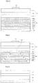
- Fig. 2 is a view of a light emitting device according to a second embodiment that is not part of the invention as claimed.
- an ohmic contact layer 60 may be disposed between the light emitting structure layer 150 of the light emitting device according to the first embodiment and the reflective metal support 80.
- the ohmic contact layer 60 may be formed of a transparent electrode layer.
- the ohmic contact layer 60 may be formed of at least one of ITO, ZnO, RuO x , TiO x , and IrO x , or at least one of Ni, Ag, and Au.
- first and second reflective metal layers 80a and 80b should have an ohmic contact characteristic with the second conductive type semiconductor layer 50.
- Each of the first and second reflective metal layers 80a and 80b are formed of at least one of Al, Ag, and APC(Ag-Pd-Cu), which have high reflectance.
- the ohmic contact layer 60 may directly contact the second conductive type semiconductor layer of the light emitting structure layer 150 and the reflective metal support 80.
- the ohmic contact layer 60 is proveded, there is a superior advantage in that the light emitting device has a superior ohmic contact characteristic with the second conductive type semiconductor layer 50.
- Fig. 3 is a view of a light emitting device according to a third embodiment that is not part of the invention as claimed.
- a solder metal layer 70 and an oxide prevention layer 100 may be disposed under the reflective metal support 80 according to the first embodiment.
- the light emitting device may be easily attached to a package body or a substrate by the solder metal layer 70.
- the solder metal layer 70 may include one of Au-Sn solder, Ag-Sn solder, and Pb-Sn solder.
- the oxide prevention layer 100 prevents the solder metal layer 70 and the reflective metal support 80 from being oxidized.
- the solder metal layer 70 may be disposed directly blow the reflective metal support 80 to contact the reflective metal support 80.
- the oxide prevention layer 100 may be disposed directly under the solder metal layer 70 to contact the solder metal layer 70.
- the oxide prevention layer 100 may contact the reflective metal support 80.
- At least one of the solder metal layer 70 and the oxide prevention layer 100 may be applicable.
- Fig. 4 is a view of a light emitting device according to a fourth embodiment.
- a current block region 110 is disposed under the light emitting structure layer 150 according to the first embodiment.
- the current block region 110 may be formed of a dielectric material or a material having low conductivity. Also, the current block region 110 may be formed of a material having a schottky contact characteristic with the second conductive type semiconductor layer 50.
- the current block region 110 vertically overlaps the electrode 90. As the current block region 110 is provided, current flowing between the reflective metal support 80 and the electrode 90 may be spread into a wide region of the active layer 40. Thus, internal quantum efficiency of the light emitting device may be improved.
- Each of the first and second reflective metal layers 80a and 80b under the current block region 110 may be spaced from the second conductive type semiconductor layer 50 corresponding to a position of the current block region 110. That is, central portions of each of first and second reflective metal layers 80a and 80b corresponding to the position of the current block region 110 may be lower than peripheral portions of each of first and second reflective metal layers 80a and 80b. Also, a portion of the first reflective metal layers 80a may be disposed on same horizontal portion with a portion of the second reflective metal layers 80b.
- the reflective metal support 80 is disposed directly under the current block region 110 to contact upper and side surfaces of the current block region 110.
- the current block region 110 may be applied to the light emitting device according to the second embodiment or the light emitting device according to the third embodiment. Also, the current block region 110 may contact the second conductive type semiconductor layer 50.
- Figs. 5 to 7 are views for explaining a process of manufacturing the light emitting device according to the first embodiment.
- an un-doped nitride layer 20 including a buffer layer is formed on a growth substrate 10.
- a light emitting structure layer 150 including a first conductive type semiconductor layer 30, an active layer 40, and a second conductive type semiconductor layer 50 is formed on the un-doped nitride layer 20.
- the growth substrate 10 may be formed of at least one of sapphire (Al 2 O 3 ), Si, SiC, GaAs, ZnO, and MgO, but is not limited thereto.
- the light emitting structure layer 150 may be grown on the growth substrate 10, and a sapphire substrate may be used as the growth substrate 10.
- a plurality of protrusion patterns may be formed on the growth substrate 10.
- the protrusion patterns may disperse light emitted from the active layer 40 to improve light efficiency.
- each of the protrusion patterns may have one of a hemisphere shape, a polygonal shape, a pyramid shape, and a nano pillar shape.
- the un-doped nitride layer 20 may be a nitride layer having a first conductive type conductivity.
- the un-doped nitride layer 20 may include an undoped-GaN layer.
- the buffer layer may be formed between the un-doped nitride layer 20 and the growth substrate 10. Also, the formation of the un-doped nitride layer 20 is not necessary, and the un-doped nitride layer 20 may not be formed.
- the un-doped nitride layer 20 may include a GaN-based semiconductor layer.
- a GaN-based semiconductor layer For example, an un-doped GaN layer grown by injecting trimethylgallium (TMGa) gas, hydrogen gas, and ammonia gas into a chamber may be used as the un-doped nitride layer.
- TMGa trimethylgallium
- Trimethylgallium (TMGa) gas, silane gas (SiH 4 ) containing and N-type impurities (e.g., Si), hydrogen gas, and ammonia gas may be injected into the chamber to grow the first conductive type semiconductor layer 30. Then, the active layer 40 and the second conductive type semiconductor layer 50 are formed on the first conductive type semiconductor layer 30.
- the active layer 40 may have a single quantum well structure or a multi quantum well (MQW) structure.
- the active layer 40 may have a stacked structure of an InGaN well layer/GaN barrier layer.
- Trimethylgallium (TMGa) gas, Bis(ethylcyclopentadienyl) magnesium (EtCp 2 Mg) ⁇ Mg(C 2 H 5 C 5 H 4 ) 2 ⁇ gas containing the and P-type impurities (e.g., Mg), hydrogen gas, and ammonia gas may be injected into the chamber to grow the second conductive type semiconductor layer 50.
- a reflective metal support 80 is formed on the second conductive type semiconductor layer 50.
- a first reflective metal layer 80a is formed on the second conductive type semiconductor layer 50, and a second reflective metal layer 80b is formed on the first reflective metal layer 80a.
- a first reflective metal layer 80a is formed again on the second reflective metal layer 80b, and a second reflective metal layer 80b is formed again on the first reflective metal layer 80a.
- the above-described processes are repeatedly performed.
- the first and second reflective metal layers 80a and 80b may be formed using a dry deposition process.
- the dry deposition process may include a sputtering process or an E-beam evaporation process.
- a high rate sputtering process may be used.
- the high rate sputtering process represents a sputtering process in which a magnetic material is disposed on a backside of a cathode sputtering target to vertically form a magnetic field in an electric field, and then, movement of electrons is restricted around the target to induce a rotation-reciprocation motion and increase a moving path, thereby increasing plasma density and improving sputtering yield.
- the first and second reflective metal layers 80a and 80b may be formed of a same metal or different metals.
- first and second reflective metal layers 80a and 80b are formed of a same metal, conditions of the sputtering process may be varied to allow the first and second reflective metal layers 80a and 80b to respectively have a tensile stress and a compressive stress, which embodiment is not part of the present invention.
- the reflective metal layer having the compressive stress may be formed.
- a process of forming the reflective metal layer having the compressive stress may include a process of increasing a sputtering power, a method of reducing a pressure of sputtering gas, a method of increasing a temperature of the substrate, and a pulse sputtering process.
- the reflective metal layer having the compressive stress is formed.
- the reflective metal layer having the tensile stress is formed.
- the sputtering power, the gas pressure, and the substrate temperature may be controlled to selectively form the reflective metal layer having the tensile stress and the reflective metal layer having the compressive stress.
- first and second metal layers 80a and 80b are formed using different materials, a metal that easily generates the tensile stress or the compressive stress may be used. Also, the first and second metal layers 80a and 80b may be formed using the process of generating the tensile stress and the compressive stress in the same metal as described above.
- the growth substrate 10 and the un-doped nitride layer 20 are removed.
- the growth substrate 10 and the un-doped nitride layer 20 may be may be removed using a laser lift off process of a chemical lift off process.
- An electrode 90 is formed on the first conductive type semiconductor layer 30 exposed by removing the growth substrate 10 and the un-doped nitride layer 20.
- the light emitting device according to the first embodiment as shown in Fig. 1 may be manufactured.
- the light emitting device according to the second embodiment may be manufactured.
- the light emitting device according to the third embodiment may be manufactured.
- Fig. 8 is a view of a light emitting device package according to an embodiment.
- a light emitting device package includes a package body 200, first and second electrodes 210 and 220 disposed on the package body 200, a light emitting device 500 disposed on the package body 200 and electrically connected to the first and second electrodes 210 and 220, and a molding member 400 surrounding the light emitting device 500.
- the package body 200 may be formed of a silicon material, a synthetic resin material, or a metal material. Also, an inclined surface may be disposed around the light emitting device 500.
- the first and second electrodes 210 and 220 are electrically separated from each other to supply power to the light emitting device 500. Also, the first and second electrodes 210 and 220 may reflect light generated in the light emitting device 500 to increase light efficiency. In addition, the first and second electrodes 210 and 220 may discharge heat generated in the light emitting device 500 to the outside.
- the light emitting device 500 may be applied to the light emitting device described in Figs. 1 to 4 .
- the light emitting device 500 may be disposed on the package body 200 or the first and second electrodes 210 and 220.
- the reflective metal support 80 may be disposed on the most weaker portion of the light emitting device 500, and only a bonding material may be disposed between the reflective metal support 80 and the package body 220 or the first and second electrodes 210 and 220.
- the light emitting device 500 may be electrically connected to the second electrode 220 through a wire 300.
- the molding member 400 may surround the light emitting device 500 to protect the light emitting device 500. Also, a phosphor may be contained in the molding member 400 to change a wavelength of the light emitted from the light emitting device 500.
- a portion 600 of light emitted from the light emitting device 500 may be fully reflected by a boundary between the molding member 400 and air. Thus, the fully reflected light may not be emitted to the outside. Then, the light reflected by the package body and incident into the light emitting device 500 may be reflected by the reflective metal support 80 of the light emitting device 500 and emitted to the outside.
- the light emitting device 500 since the light emitting device 500 includes the reflective metal support 80 having superior reflectance under the light emitting structure layer 150, the light emitting device 500 may have high light emitting efficiency when compared that a conductive support substrate having low reflectance instead of the reflective metal support 80 is used.
- the light emitting device package may include a chip on board (COB) type light emitting device package.
- the package body 200 may have a flat top surface, and a plurality of light emitting devices 500 may be disposed on the package body 200.
- COB chip on board
- the light emitting device may be provided in plurality.
- the plurality of light emitting devices may be arrayed on the substrate.
- Optical members such as a light guide plate, a prism sheet, a diffusion sheet, and a fluorescence sheet may be disposed on a path of the light emitted from the light emitting device packages.
- the light emitting device package, the substrate, and the optical members may function as a backlight unit.
- the light emitting device 500 or the light emitting device package according to the above-described embodiments may be realized as a lighting unit.
- the lighting unit may include a display device, an indicating device, a lamp, and a street lamp.
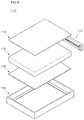
- Fig. 9 is a view of a backlight unit using a light emitting device or a light emitting device package according to an embodiment.
- the backlight unit 1100 of the Fig. 9 is an example of a lighting system, and the present disclosure is not limited thereto.
- the backlight unit 1100 may include a bottom cover 1140, a light guide member 1120 disposed within the bottom cover 1140, and a light emitting module 1110 disposed on at least one side or an under surface of the light guide member 1120. Also, a reflective sheet 1130 may be disposed under the light guide member 1120.
- the bottom cover 1140 may have a box shape with an opened upper side to receive the light guide member 1120, the light emitting module 1110, and the reflective sheet 1130.
- the bottom cover 1140 may be formed of a metal material or a resin material, but is not limited thereto.
- the light emitting module 1110 may include a substrate and a plurality of light emitting device or light emitting device packages, which are mounted on the substrate.
- the plurality of light emitting device or light emitting device packages may provide light to the light guide member 1120.
- the light emitting module 1110 may be disposed on at least one of inner surfaces of the bottom cover 1140. Thus, the light emitting module 1110 may provide light toward at least one lateral surface of the light guide member 1120.
- the light emitting module 1110 may be disposed on an under surface the light guide member 1120 to provide light toward the under surface of the light guide member 1120. This may be variously varied according to a design of the backlight unit 1100, and thus, the present disclosure is not limited thereto.
- the light guide member 1120 may be disposed within the bottom cover 1140.
- the light guide member 1120 may receive the light provided from the light emitting module 1110 to produce planar light, thereby guiding the planar light to a display panel (not shown).
- the light guide member 1120 may be a light guide panel (LGP).
- the LGP may be formed of one of a resin-based material such as polymethylmethacrylate (PMMA), a polyethylene terephthalate (PET) resin, a poly carbonate (PC) resin, a cyclic olefin copolymer (COC) resin, and a polyethylene naphthalate (PEN) resin.
- PMMA polymethylmethacrylate
- PET polyethylene terephthalate
- PC poly carbonate
- COC cyclic olefin copolymer
- PEN polyethylene naphthalate
- An optical sheet 1150 may be disposed above the light guide member 1120.
- the optical sheet 1150 may include at least one of a diffusion sheet, a light collection sheet, a brightness enhancement sheet, and a fluorescence sheet.
- the diffusion sheet, the light collection sheet, the brightness enhancement sheet, and the fluorescence sheet may be stacked to form the optical sheet 1150.
- the diffusion sheet 1150 may uniformly diffuse light emitted from the light emitting module 1110, and the diffused light may be collected into the display panel (not shown) by the light collection sheet.
- the light emitted from the light collection sheet is randomly polarized light.
- the bright enhancement sheet may enhance a degree of polarization of the light emitted from the light collection sheet.
- the light collection sheet may be a horizontal and/or vertical prism sheet.
- the bright enhancement sheet may be a dual brightness enhancement film.
- the fluorescence sheet may be a light transmitting plate or film including a phosphor.
- the reflective sheet 1130 may be disposed under the light guide member 1120.
- the reflective sheet 1130 reflects the light emitted through the under surface of the light guide member 1120 toward a light emitting surface of the light guide member 1120.
- the reflective sheet 1130 may be formed of a material having superior reflectance, e.g., a PET resin, a PC resin, or a PVC resin, but is not limited thereto.
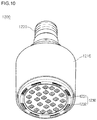
- Fig. 10 is a view of a lighting unit using a light emitting device or a light emitting device package according to an embodiment.
- the lighting unit 1200 of Fig. 10 is an example of a lighting system, and thus, the present disclosure is not limited thereto.
- the lighting system 1200 may include a case body 1210, a light emitting module 1230 disposed on the case body 1210, a connection terminal 1220 disposed on the case body 1210 to receive power from an external power source.
- the case body 1210 may be formed of a material having good thermal dissipation properties, e.g., a metal material or a resin material.
- the light emitting module 1230 may include a substrate 1232 and at least one light emitting device package 1231 mounted on the substrate 1232.
- a circuit pattern may be printed on a dielectric to form the substrate 1232.
- the substrate 1232 may include a printed circuit board (PCB), a metal core PCB, a flexible PCB, and a ceramic PCB.
- PCB printed circuit board
- metal core PCB metal core PCB
- flexible PCB flexible PCB
- ceramic PCB ceramic PCB
- the substrate 1232 may be formed of an effectively reflective material or have a color on which light is effectively reflected from a surface thereof, e.g., a white color or a silver color.
- At least one light emitting device package 1231 may be mounted on the substrate 1232.
- the light emitting device package 1231 may include at least one light emitting diode (LED).
- the LED may include colored LEDs, which respectively emit light having a red color, a green color, a blue color, and a white color and an ultraviolet (UV) LED emitting UV rays.
- UV ultraviolet
- the light emitting module 1230 may have various combinations of the LED to obtain color impression and brightness.
- the white LED, the red LED, and the green LED may be combined with each other to secure a high color rendering index.
- a fluorescence sheet may be further disposed on a path of light emitted from the light emitting module 1230.
- the fluorescence sheet changes a wavelength of the light emitted from the light emitting module 1230.
- the fluorescence sheet may include a yellow phosphor.
- the light emitted from the light emitting module 1230 passes through the fluorescence sheet to finally emit white light.
- connection terminal 1220 may be electrically connected to the light emitting module 1230 to provide a power to the light emitting module 1230.
- the connected terminal 1220 is screw-coupled to an external power source in a socket manner, but is not limited thereto.
- the connection terminal 1220 may have a pin shape, and thus, be inserted into the external power source.
- the connection terminal 1220 may be connected to the external power source by a wire.
- any reference in this specification to "one embodiment,” “an embodiment,” “example embodiment,” etc. means that a particular feature, structure, or characteristic described in connection with the embodiment is included in at least one embodiment of the invention.
- the appearances of such phrases in various places in the specification are not necessarily all referring to the same embodiment.
Landscapes
- Led Devices (AREA)
- Led Device Packages (AREA)
Claims (14)
- Lichtemittierende Vorrichtung, die aufweist:einen reflektierenden Metallträger (80) mit mindestens zwei Paaren erster und zweiter reflektierender Metallschichten,eine lichtemittierende Strukturschicht (150) mit einer Halbleiterschicht (30) vom ersten Leitfähigkeitstyp, einer Halbleiterschicht (50) vom zweiten Leitfähigkeitstyp und einer aktiven Schicht (40) zwischen der Halbleiterschicht (30) vom ersten Leitfähigkeitstyp und der Halbleiterschicht (50) vom zweiten Leitfähigkeitstyp auf dem reflektierenden Metallträger (80);eine Elektrode (90) auf der lichtemittierenden Strukturschicht (150); undeinen unter der lichtemittierenden Strukturschicht (150) angeordneten Stromsperrbereich (110), wobeider Stromsperrbereich (110) die Elektrode (90) vertikal überlappt,wobei die lichtemittierende Strukturschicht (150) ein blaues Licht emittiert,wobei der reflektierende Metallträger (80) ein von der lichtemittierenden Strukturschicht (150) emittiertes Licht reflektiert,wobei der reflektierende Metallträger (80) 30 Paare bis 70 Paare der ersten und zweiten reflektierenden Metallschichten (80a und 80b) aufweist,wobei jede der ersten und zweiten reflektierenden Metallschichten aus mindestens einem Element ausgewählt aus Al, Ag, einer APC- (Ag-Pd-Cu) Legierung und einer Au-Ni-Legierung gebildet ist,wobei die ersten und zweiten reflektierenden Metallschichten, die aufeinander gestapelt sind, aus verschiedenen Materialien gebildet werden,wobei der reflektierende Metallträger (80) eine Dicke von 50 µm bis 200 µm aufweist undwobei die erste reflektierende Metallschicht eine Druckspannung aufweist und die zweite reflektierende Metallschicht eine Zugspannung aufweist.
- Lichtemittierende Vorrichtung nach Anspruch 1, ferner aufweisend eine ohmsche Kontaktschicht (60) zwischen dem reflektierenden Metallträger (80) und der lichtemittierenden Strukturschicht (150).
- Lichtemittierende Vorrichtung nach Anspruch 1, wobei der reflektierende Metallträger (80) eine Au-Ni-Legierungsschicht aufweist, die direkt unter der Halbleiterschicht (50) vom zweiten Leitfähigkeitstyp angeordnet ist, um die Halbleiterschicht (50) vom zweiten Leitfähigkeitstyp zu berühren.
- Lichtemittierende Vorrichtung nach einem der Ansprüche 1 bis 3, wobei der Stromsperrbereich (100) zwischen dem reflektierenden Metallträger (80) und der lichtemittierenden Strukturschicht (150) angeordnet ist.
- Lichtemittierende Vorrichtung nach einem der Ansprüche 1 bis 4, wobei jede der ersten und zweiten reflektierenden Metallschichten (80a, 80b) einen Abschnitt aufweist, der der Position des Stromsperrbereichs (110) entspricht, der niedriger als ein Umfangsabschnitt jeder der ersten und zweiten reflektierenden Metallschichten (80a, 80b) ist.
- Lichtemittierende Vorrichtung nach einem der Ansprüche 1 bis 5, ferner aufweisend eine Lötmetallschicht unter dem reflektierenden Metallträger,
wobei die Lötmetallschicht (70) den reflektierenden Metallträger (80) direkt berührt. - Lichtemittierende Vorrichtung nach Anspruch 6, ferner aufweisend eine Oxidverhinderungsschicht unter der Lötmetallschicht.
- Lichtemittierende Vorrichtung nach einem der Ansprüche 1 bis 7, wobei der reflektierende Metallträger eine Dicke aufweist, die dicker als die der lichtemittierenden Strukturschicht ist.
- Lichtemittierende Vorrichtung nach einem der Ansprüche 1 bis 8, wobei jede der ersten und zweiten reflektierenden Metallschichten eine Dicke von 0,1 µm bis 10 µm hat.
- Lichtemittierende Vorrichtung nach einem der Ansprüche 1 bis 9,
wobei die erste reflektierende Metallschicht (80a) eine Druckspannung von 100 MPa bis 2.000 MPa aufweist und die zweite reflektierende Metallschicht (80b) eine Zugspannung von 100 MPa bis 2.000 MPa aufweist und
wobei der reflektierende Metallträger (80) 40 Paare bis 80 Paare der ersten und zweiten reflektierenden Metallschichten (80a und 80b) aufweist. - Lichtemittierende Vorrichtung nach einem der Ansprüche 1 bis 10, wobei der reflektierende Metallträger (80) direkt unter dem Stromsperrbereich (110) angeordnet ist, um die Oberseite und Seitenflächen des Stromsperrbereichs (110) zu berühren.
- Lichtemittierende Vorrichtung nach einem der Ansprüche 1 bis 11, wobei der Stromsperrbereich (110) aus einem dielektrischen Material oder einem Material gebildet ist, das eine geringe Leitfähigkeit oder Schottky-Kontakteigenschaften mit der Halbleiterschicht (50) vom zweiten Leitfähigkeitstyp aufweist.
- Lichtemittierende Vorrichtungsbaugruppe, die aufweist:einen Baugruppenkörper;eine erste und eine zweite Elektrode auf dem Baugruppenkörper;eine lichtemittierende Vorrichtung nach einem der Ansprüche 1 bis 12, wobei die lichtemittierende Vorrichtung elektrisch mit der ersten und der zweiten Elektrode auf dem Baugruppenkörper verbunden ist; undein Formelement, das die lichtemittierende Vorrichtung auf dem Baugruppenkörper umgibt.
- Beleuchtungssystem, das eine lichtemittierende Vorrichtung als Lichtquelle verwendet, wobei das Beleuchtungssystem aufweist:ein Substrat; undmindestens eine lichtemittierende Vorrichtung nach einem der Ansprüche 1 bis 12, wobei die mindestens eine lichtemittierende Vorrichtung auf dem Substrat angeordnet ist.
Applications Claiming Priority (1)
| Application Number | Priority Date | Filing Date | Title |
|---|---|---|---|
| KR20100020922A KR101055003B1 (ko) | 2010-03-09 | 2010-03-09 | 발광 소자, 발광 소자 패키지, 조명 시스템, 및 발광 소자 제조방법 |
Publications (3)
| Publication Number | Publication Date |
|---|---|
| EP2365545A2 EP2365545A2 (de) | 2011-09-14 |
| EP2365545A3 EP2365545A3 (de) | 2015-04-08 |
| EP2365545B1 true EP2365545B1 (de) | 2019-08-28 |
Family
ID=44065323
Family Applications (1)
| Application Number | Title | Priority Date | Filing Date |
|---|---|---|---|
| EP10193392.7A Not-in-force EP2365545B1 (de) | 2010-03-09 | 2010-12-01 | Lichtemittierende Vorrichtung, Gehäuse für lichtemittierende Vorrichtung und Beleuchtungssystem |
Country Status (4)
| Country | Link |
|---|---|
| US (1) | US8735921B2 (de) |
| EP (1) | EP2365545B1 (de) |
| KR (1) | KR101055003B1 (de) |
| CN (1) | CN102194936B (de) |
Families Citing this family (8)
| Publication number | Priority date | Publication date | Assignee | Title |
|---|---|---|---|---|
| KR101055003B1 (ko) * | 2010-03-09 | 2011-08-05 | 엘지이노텍 주식회사 | 발광 소자, 발광 소자 패키지, 조명 시스템, 및 발광 소자 제조방법 |
| KR101414645B1 (ko) * | 2011-10-28 | 2014-07-03 | 엘지전자 주식회사 | 수직형 질화물계 반도체 발광 소자 및 그 제조 방법 |
| CN107850705B (zh) * | 2015-07-27 | 2020-02-14 | 柯尼卡美能达株式会社 | 银反射镜以及其制造方法及检查方法 |
| DE102018103291A1 (de) * | 2018-02-14 | 2019-08-14 | Osram Opto Semiconductors Gmbh | Optoelektronisches halbleiterbauteil und verfahren zur herstellung eines optoelektronischen halbleiterbauteils |
| CN116685714B (zh) | 2021-12-29 | 2026-04-10 | 京东方科技集团股份有限公司 | 线路板、功能背板、背光模组、显示面板及显示装置 |
| US12581596B2 (en) | 2021-12-31 | 2026-03-17 | Boe Technology Group Co., Ltd. | Wiring board, functional backplane and method for manufacturing the same |
| US12610675B2 (en) | 2022-04-21 | 2026-04-21 | Boe Technology Group Co., Ltd. | Circuit board, light-emitting substrate, backlight module, display panel and display device |
| WO2024092439A1 (zh) | 2022-10-31 | 2024-05-10 | 京东方科技集团股份有限公司 | 线路板、发光基板、背光模组及显示装置 |
Citations (2)
| Publication number | Priority date | Publication date | Assignee | Title |
|---|---|---|---|---|
| US20090008668A1 (en) * | 2007-07-03 | 2009-01-08 | Nichia Corporation | Semiconductor Light Emitting Device and Method for Fabricating the Same |
| EP2348547A2 (de) * | 2010-01-21 | 2011-07-27 | LG Innotek Co., Ltd. | Lichtemittierende Vorrichtung, Verfahren zu deren Herstellung, Verpackung für lichtemittierende Vorrichtung und Beleuchtungssystem |
Family Cites Families (27)
| Publication number | Priority date | Publication date | Assignee | Title |
|---|---|---|---|---|
| JP3102647B2 (ja) * | 1990-12-10 | 2000-10-23 | 日本電信電話株式会社 | 半導体発光素子 |
| US6134049A (en) * | 1998-09-25 | 2000-10-17 | The Regents Of The University Of California | Method to adjust multilayer film stress induced deformation of optics |
| DE10041328B4 (de) * | 2000-08-23 | 2018-04-05 | Osram Opto Semiconductors Gmbh | Verpackungseinheit für Halbleiterchips |
| JP4960665B2 (ja) * | 2006-08-11 | 2012-06-27 | キヤノン株式会社 | 発光素子アレイ及び画像形成装置 |
| CN1372328A (zh) * | 2001-02-26 | 2002-10-02 | 连威磊晶科技股份有限公司 | 具有光学反射膜的发光二极管 |
| JP3991193B2 (ja) | 2001-11-05 | 2007-10-17 | サンケン電気株式会社 | 半導体発光素子 |
| JP4806678B2 (ja) * | 2004-05-17 | 2011-11-02 | トムソン ライセンシング | 光取り出しが改善された有機発光ダイオード(oled)及びそれに対応するディスプレイユニット |
| JP2006135215A (ja) | 2004-11-09 | 2006-05-25 | Hitachi Cable Ltd | 半導体発光素子の製造方法 |
| TW200707799A (en) * | 2005-04-21 | 2007-02-16 | Aonex Technologies Inc | Bonded intermediate substrate and method of making same |
| KR101365621B1 (ko) * | 2007-09-04 | 2014-02-24 | 서울반도체 주식회사 | 열 방출 슬러그들을 갖는 발광 다이오드 패키지 |
| KR20090027329A (ko) * | 2007-09-12 | 2009-03-17 | 삼성전기주식회사 | 수직구조 반도체 발광소자 및 그 제조 방법 |
| WO2009078574A1 (en) * | 2007-12-18 | 2009-06-25 | Seoul Opto Device Co., Ltd. | Light emitting device and method of manufacturing the same |
| KR101393355B1 (ko) | 2007-12-28 | 2014-06-30 | 서울바이오시스 주식회사 | 발광 다이오드 및 그 제조방법 |
| WO2009084857A2 (en) * | 2007-12-28 | 2009-07-09 | Seoul Opto Device Co., Ltd. | Light emitting diode and method of fabricating the same |
| KR20090072980A (ko) * | 2007-12-28 | 2009-07-02 | 서울옵토디바이스주식회사 | 발광 다이오드 및 그 제조방법 |
| KR20100036758A (ko) | 2008-09-30 | 2010-04-08 | 서울옵토디바이스주식회사 | 발광 다이오드 및 그 제조 방법 |
| KR101650840B1 (ko) * | 2009-08-26 | 2016-08-24 | 삼성전자주식회사 | 발광소자 및 이의 제조방법 |
| KR101072034B1 (ko) * | 2009-10-15 | 2011-10-10 | 엘지이노텍 주식회사 | 반도체 발광소자 및 그 제조방법 |
| KR101662037B1 (ko) * | 2009-12-02 | 2016-10-05 | 삼성전자 주식회사 | 발광 소자 및 그 제조 방법 |
| KR101055003B1 (ko) * | 2010-03-09 | 2011-08-05 | 엘지이노텍 주식회사 | 발광 소자, 발광 소자 패키지, 조명 시스템, 및 발광 소자 제조방법 |
| US8618565B2 (en) * | 2010-03-22 | 2013-12-31 | Seoul Opto Device Co., Ltd. | High efficiency light emitting diode |
| US8772805B2 (en) * | 2010-03-31 | 2014-07-08 | Seoul Viosys Co., Ltd. | High efficiency light emitting diode and method for fabricating the same |
| KR101034053B1 (ko) * | 2010-05-25 | 2011-05-12 | 엘지이노텍 주식회사 | 발광 소자, 발광 소자 제조방법 및 발광 소자 패키지 |
| WO2011162479A2 (en) * | 2010-06-24 | 2011-12-29 | Seoul Opto Device Co., Ltd. | Light emitting diode |
| KR20120126856A (ko) * | 2011-05-13 | 2012-11-21 | 삼성전자주식회사 | 반도체 발광다이오드 칩 및 이를 이용한 발광장치 |
| KR101941029B1 (ko) * | 2011-06-30 | 2019-01-22 | 엘지이노텍 주식회사 | 발광소자 및 이를 포함하는 조명시스템 |
| KR101791175B1 (ko) * | 2011-06-30 | 2017-10-27 | 엘지이노텍 주식회사 | 발광소자 및 이를 포함하는 발광소자 패키지 |
-
2010
- 2010-03-09 KR KR20100020922A patent/KR101055003B1/ko not_active Expired - Fee Related
- 2010-12-01 EP EP10193392.7A patent/EP2365545B1/de not_active Not-in-force
- 2010-12-02 US US12/959,102 patent/US8735921B2/en active Active
- 2010-12-30 CN CN201010622063.2A patent/CN102194936B/zh not_active Expired - Fee Related
Patent Citations (2)
| Publication number | Priority date | Publication date | Assignee | Title |
|---|---|---|---|---|
| US20090008668A1 (en) * | 2007-07-03 | 2009-01-08 | Nichia Corporation | Semiconductor Light Emitting Device and Method for Fabricating the Same |
| EP2348547A2 (de) * | 2010-01-21 | 2011-07-27 | LG Innotek Co., Ltd. | Lichtemittierende Vorrichtung, Verfahren zu deren Herstellung, Verpackung für lichtemittierende Vorrichtung und Beleuchtungssystem |
Also Published As
| Publication number | Publication date |
|---|---|
| US20110220940A1 (en) | 2011-09-15 |
| KR101055003B1 (ko) | 2011-08-05 |
| CN102194936A (zh) | 2011-09-21 |
| CN102194936B (zh) | 2015-07-22 |
| EP2365545A3 (de) | 2015-04-08 |
| EP2365545A2 (de) | 2011-09-14 |
| US8735921B2 (en) | 2014-05-27 |
Similar Documents
| Publication | Publication Date | Title |
|---|---|---|
| KR101081062B1 (ko) | 발광 소자, 발광 소자 제조방법 및 발광 소자 패키지 | |
| US8698176B2 (en) | Light emitting device and lighting system | |
| TWI470825B (zh) | 發光裝置及其製造方法 | |
| CN102222741B (zh) | 发光器件和发光器件封装 | |
| EP2365545B1 (de) | Lichtemittierende Vorrichtung, Gehäuse für lichtemittierende Vorrichtung und Beleuchtungssystem | |
| EP2355196B1 (de) | Gehäuse für lichtemittierende Vorrichtung, Verfahren zu dessen Herstellung und Beleuchtungssystem | |
| EP2333851B1 (de) | Lichtemittierende Vorrichtung, Gehäuse für lichtemittierende Vorrichtung und Beleuchtungssystem | |
| KR101798231B1 (ko) | 발광 소자 | |
| KR20120003775A (ko) | 발광 소자, 발광 소자 제조방법, 발광 소자 패키지, 및 조명 시스템 | |
| US20110108868A1 (en) | Light emitting device, light emitting device package and lighting system | |
| US8350274B2 (en) | Light emitting device, method of manufacturing the light emitting device, light emitting device package, and lighting unit | |
| KR20140097898A (ko) | 발광소자 | |
| US20110186882A1 (en) | Light emitting device, method of fabricating the light emitting device, light emitting device package, and lighting system | |
| KR20130028291A (ko) | 발광소자 및 발광 소자 패키지 | |
| KR101907618B1 (ko) | 발광소자 | |
| KR101865405B1 (ko) | 발광소자 | |
| KR20110139445A (ko) | 발광 소자, 발광 소자 제조방법, 발광 소자 패키지 및 조명 시스템 | |
| KR20160124065A (ko) | 발광 소자, 발광 소자 패키지 및 조명 시스템 | |
| KR20150028081A (ko) | 발광소자 | |
| KR20130059137A (ko) | 발광소자 | |
| KR20120116153A (ko) | 발광소자패키지 | |
| KR20130056367A (ko) | 발광 소자 | |
| KR20150028924A (ko) | 발광소자 | |
| KR20130031673A (ko) | 발광소자, 발광소자 패키지, 조명 시스템 및 발광소자 제조방법 |
Legal Events
| Date | Code | Title | Description |
|---|---|---|---|
| PUAI | Public reference made under article 153(3) epc to a published international application that has entered the european phase |
Free format text: ORIGINAL CODE: 0009012 |
|
| AK | Designated contracting states |
Kind code of ref document: A2 Designated state(s): AL AT BE BG CH CY CZ DE DK EE ES FI FR GB GR HR HU IE IS IT LI LT LU LV MC MK MT NL NO PL PT RO RS SE SI SK SM TR |
|
| AX | Request for extension of the european patent |
Extension state: BA ME |
|
| 17P | Request for examination filed |
Effective date: 20140328 |
|
| RBV | Designated contracting states (corrected) |
Designated state(s): AL AT BE BG CH CY CZ DE DK EE ES FI FR GB GR HR HU IE IS IT LI LT LU LV MC MK MT NL NO PL PT RO RS SE SI SK SM TR |
|
| RAP1 | Party data changed (applicant data changed or rights of an application transferred) |
Owner name: LG INNOTEK CO., LTD. |
|
| PUAL | Search report despatched |
Free format text: ORIGINAL CODE: 0009013 |
|
| AK | Designated contracting states |
Kind code of ref document: A3 Designated state(s): AL AT BE BG CH CY CZ DE DK EE ES FI FR GB GR HR HU IE IS IT LI LT LU LV MC MK MT NL NO PL PT RO RS SE SI SK SM TR |
|
| AX | Request for extension of the european patent |
Extension state: BA ME |
|
| RIC1 | Information provided on ipc code assigned before grant |
Ipc: H01L 33/40 20100101AFI20150227BHEP Ipc: G02B 5/08 20060101ALN20150227BHEP |
|
| RAP1 | Party data changed (applicant data changed or rights of an application transferred) |
Owner name: LG INNOTEK CO., LTD. |
|
| STAA | Information on the status of an ep patent application or granted ep patent |
Free format text: STATUS: EXAMINATION IS IN PROGRESS |
|
| 17Q | First examination report despatched |
Effective date: 20180319 |
|
| GRAP | Despatch of communication of intention to grant a patent |
Free format text: ORIGINAL CODE: EPIDOSNIGR1 |
|
| STAA | Information on the status of an ep patent application or granted ep patent |
Free format text: STATUS: GRANT OF PATENT IS INTENDED |
|
| RIC1 | Information provided on ipc code assigned before grant |
Ipc: G02B 5/08 20060101ALN20181030BHEP Ipc: H01L 33/40 20100101AFI20181030BHEP |
|
| RIC1 | Information provided on ipc code assigned before grant |
Ipc: G02B 5/08 20060101ALN20181116BHEP Ipc: H01L 33/40 20100101AFI20181116BHEP |
|
| INTG | Intention to grant announced |
Effective date: 20181204 |
|
| GRAS | Grant fee paid |
Free format text: ORIGINAL CODE: EPIDOSNIGR3 |
|
| GRAJ | Information related to disapproval of communication of intention to grant by the applicant or resumption of examination proceedings by the epo deleted |
Free format text: ORIGINAL CODE: EPIDOSDIGR1 |
|
| GRAL | Information related to payment of fee for publishing/printing deleted |
Free format text: ORIGINAL CODE: EPIDOSDIGR3 |
|
| STAA | Information on the status of an ep patent application or granted ep patent |
Free format text: STATUS: EXAMINATION IS IN PROGRESS |
|
| GRAP | Despatch of communication of intention to grant a patent |
Free format text: ORIGINAL CODE: EPIDOSNIGR1 |
|
| STAA | Information on the status of an ep patent application or granted ep patent |
Free format text: STATUS: GRANT OF PATENT IS INTENDED |
|
| INTC | Intention to grant announced (deleted) | ||
| INTG | Intention to grant announced |
Effective date: 20190515 |
|
| RIC1 | Information provided on ipc code assigned before grant |
Ipc: H01L 33/40 20100101AFI20190507BHEP Ipc: G02B 5/08 20060101ALN20190507BHEP |
|
| GRAA | (expected) grant |
Free format text: ORIGINAL CODE: 0009210 |
|
| STAA | Information on the status of an ep patent application or granted ep patent |
Free format text: STATUS: THE PATENT HAS BEEN GRANTED |
|
| AK | Designated contracting states |
Kind code of ref document: B1 Designated state(s): AL AT BE BG CH CY CZ DE DK EE ES FI FR GB GR HR HU IE IS IT LI LT LU LV MC MK MT NL NO PL PT RO RS SE SI SK SM TR |
|
| REG | Reference to a national code |
Ref country code: GB Ref legal event code: FG4D |
|
| REG | Reference to a national code |
Ref country code: CH Ref legal event code: EP |
|
| REG | Reference to a national code |
Ref country code: AT Ref legal event code: REF Ref document number: 1173482 Country of ref document: AT Kind code of ref document: T Effective date: 20190915 |
|
| REG | Reference to a national code |
Ref country code: IE Ref legal event code: FG4D |
|
| REG | Reference to a national code |
Ref country code: DE Ref legal event code: R096 Ref document number: 602010060749 Country of ref document: DE |
|
| REG | Reference to a national code |
Ref country code: NL Ref legal event code: MP Effective date: 20190828 |
|
| REG | Reference to a national code |
Ref country code: LT Ref legal event code: MG4D |
|
| PG25 | Lapsed in a contracting state [announced via postgrant information from national office to epo] |
Ref country code: NL Free format text: LAPSE BECAUSE OF FAILURE TO SUBMIT A TRANSLATION OF THE DESCRIPTION OR TO PAY THE FEE WITHIN THE PRESCRIBED TIME-LIMIT Effective date: 20190828 Ref country code: BG Free format text: LAPSE BECAUSE OF FAILURE TO SUBMIT A TRANSLATION OF THE DESCRIPTION OR TO PAY THE FEE WITHIN THE PRESCRIBED TIME-LIMIT Effective date: 20191128 Ref country code: NO Free format text: LAPSE BECAUSE OF FAILURE TO SUBMIT A TRANSLATION OF THE DESCRIPTION OR TO PAY THE FEE WITHIN THE PRESCRIBED TIME-LIMIT Effective date: 20191128 Ref country code: PT Free format text: LAPSE BECAUSE OF FAILURE TO SUBMIT A TRANSLATION OF THE DESCRIPTION OR TO PAY THE FEE WITHIN THE PRESCRIBED TIME-LIMIT Effective date: 20191230 Ref country code: FI Free format text: LAPSE BECAUSE OF FAILURE TO SUBMIT A TRANSLATION OF THE DESCRIPTION OR TO PAY THE FEE WITHIN THE PRESCRIBED TIME-LIMIT Effective date: 20190828 Ref country code: LT Free format text: LAPSE BECAUSE OF FAILURE TO SUBMIT A TRANSLATION OF THE DESCRIPTION OR TO PAY THE FEE WITHIN THE PRESCRIBED TIME-LIMIT Effective date: 20190828 Ref country code: SE Free format text: LAPSE BECAUSE OF FAILURE TO SUBMIT A TRANSLATION OF THE DESCRIPTION OR TO PAY THE FEE WITHIN THE PRESCRIBED TIME-LIMIT Effective date: 20190828 Ref country code: HR Free format text: LAPSE BECAUSE OF FAILURE TO SUBMIT A TRANSLATION OF THE DESCRIPTION OR TO PAY THE FEE WITHIN THE PRESCRIBED TIME-LIMIT Effective date: 20190828 |
|
| PG25 | Lapsed in a contracting state [announced via postgrant information from national office to epo] |
Ref country code: AL Free format text: LAPSE BECAUSE OF FAILURE TO SUBMIT A TRANSLATION OF THE DESCRIPTION OR TO PAY THE FEE WITHIN THE PRESCRIBED TIME-LIMIT Effective date: 20190828 Ref country code: LV Free format text: LAPSE BECAUSE OF FAILURE TO SUBMIT A TRANSLATION OF THE DESCRIPTION OR TO PAY THE FEE WITHIN THE PRESCRIBED TIME-LIMIT Effective date: 20190828 Ref country code: RS Free format text: LAPSE BECAUSE OF FAILURE TO SUBMIT A TRANSLATION OF THE DESCRIPTION OR TO PAY THE FEE WITHIN THE PRESCRIBED TIME-LIMIT Effective date: 20190828 Ref country code: GR Free format text: LAPSE BECAUSE OF FAILURE TO SUBMIT A TRANSLATION OF THE DESCRIPTION OR TO PAY THE FEE WITHIN THE PRESCRIBED TIME-LIMIT Effective date: 20191129 Ref country code: IS Free format text: LAPSE BECAUSE OF FAILURE TO SUBMIT A TRANSLATION OF THE DESCRIPTION OR TO PAY THE FEE WITHIN THE PRESCRIBED TIME-LIMIT Effective date: 20191228 Ref country code: ES Free format text: LAPSE BECAUSE OF FAILURE TO SUBMIT A TRANSLATION OF THE DESCRIPTION OR TO PAY THE FEE WITHIN THE PRESCRIBED TIME-LIMIT Effective date: 20190828 |
|
| REG | Reference to a national code |
Ref country code: AT Ref legal event code: MK05 Ref document number: 1173482 Country of ref document: AT Kind code of ref document: T Effective date: 20190828 |
|
| PG25 | Lapsed in a contracting state [announced via postgrant information from national office to epo] |
Ref country code: TR Free format text: LAPSE BECAUSE OF FAILURE TO SUBMIT A TRANSLATION OF THE DESCRIPTION OR TO PAY THE FEE WITHIN THE PRESCRIBED TIME-LIMIT Effective date: 20190828 |
|
| PG25 | Lapsed in a contracting state [announced via postgrant information from national office to epo] |
Ref country code: IT Free format text: LAPSE BECAUSE OF FAILURE TO SUBMIT A TRANSLATION OF THE DESCRIPTION OR TO PAY THE FEE WITHIN THE PRESCRIBED TIME-LIMIT Effective date: 20190828 Ref country code: DK Free format text: LAPSE BECAUSE OF FAILURE TO SUBMIT A TRANSLATION OF THE DESCRIPTION OR TO PAY THE FEE WITHIN THE PRESCRIBED TIME-LIMIT Effective date: 20190828 Ref country code: EE Free format text: LAPSE BECAUSE OF FAILURE TO SUBMIT A TRANSLATION OF THE DESCRIPTION OR TO PAY THE FEE WITHIN THE PRESCRIBED TIME-LIMIT Effective date: 20190828 Ref country code: AT Free format text: LAPSE BECAUSE OF FAILURE TO SUBMIT A TRANSLATION OF THE DESCRIPTION OR TO PAY THE FEE WITHIN THE PRESCRIBED TIME-LIMIT Effective date: 20190828 Ref country code: PL Free format text: LAPSE BECAUSE OF FAILURE TO SUBMIT A TRANSLATION OF THE DESCRIPTION OR TO PAY THE FEE WITHIN THE PRESCRIBED TIME-LIMIT Effective date: 20190828 Ref country code: RO Free format text: LAPSE BECAUSE OF FAILURE TO SUBMIT A TRANSLATION OF THE DESCRIPTION OR TO PAY THE FEE WITHIN THE PRESCRIBED TIME-LIMIT Effective date: 20190828 |
|
| PG25 | Lapsed in a contracting state [announced via postgrant information from national office to epo] |
Ref country code: CZ Free format text: LAPSE BECAUSE OF FAILURE TO SUBMIT A TRANSLATION OF THE DESCRIPTION OR TO PAY THE FEE WITHIN THE PRESCRIBED TIME-LIMIT Effective date: 20190828 Ref country code: SM Free format text: LAPSE BECAUSE OF FAILURE TO SUBMIT A TRANSLATION OF THE DESCRIPTION OR TO PAY THE FEE WITHIN THE PRESCRIBED TIME-LIMIT Effective date: 20190828 Ref country code: SK Free format text: LAPSE BECAUSE OF FAILURE TO SUBMIT A TRANSLATION OF THE DESCRIPTION OR TO PAY THE FEE WITHIN THE PRESCRIBED TIME-LIMIT Effective date: 20190828 Ref country code: IS Free format text: LAPSE BECAUSE OF FAILURE TO SUBMIT A TRANSLATION OF THE DESCRIPTION OR TO PAY THE FEE WITHIN THE PRESCRIBED TIME-LIMIT Effective date: 20200224 |
|
| REG | Reference to a national code |
Ref country code: DE Ref legal event code: R097 Ref document number: 602010060749 Country of ref document: DE |
|
| PLBE | No opposition filed within time limit |
Free format text: ORIGINAL CODE: 0009261 |
|
| STAA | Information on the status of an ep patent application or granted ep patent |
Free format text: STATUS: NO OPPOSITION FILED WITHIN TIME LIMIT |
|
| PG2D | Information on lapse in contracting state deleted |
Ref country code: IS |
|
| REG | Reference to a national code |
Ref country code: CH Ref legal event code: PL |
|
| 26N | No opposition filed |
Effective date: 20200603 |
|
| REG | Reference to a national code |
Ref country code: BE Ref legal event code: MM Effective date: 20191231 |
|
| PG25 | Lapsed in a contracting state [announced via postgrant information from national office to epo] |
Ref country code: SI Free format text: LAPSE BECAUSE OF FAILURE TO SUBMIT A TRANSLATION OF THE DESCRIPTION OR TO PAY THE FEE WITHIN THE PRESCRIBED TIME-LIMIT Effective date: 20190828 Ref country code: MC Free format text: LAPSE BECAUSE OF FAILURE TO SUBMIT A TRANSLATION OF THE DESCRIPTION OR TO PAY THE FEE WITHIN THE PRESCRIBED TIME-LIMIT Effective date: 20190828 |
|
| GBPC | Gb: european patent ceased through non-payment of renewal fee |
Effective date: 20191201 |
|
| PG25 | Lapsed in a contracting state [announced via postgrant information from national office to epo] |
Ref country code: GB Free format text: LAPSE BECAUSE OF NON-PAYMENT OF DUE FEES Effective date: 20191201 Ref country code: FR Free format text: LAPSE BECAUSE OF NON-PAYMENT OF DUE FEES Effective date: 20191231 Ref country code: LU Free format text: LAPSE BECAUSE OF NON-PAYMENT OF DUE FEES Effective date: 20191201 Ref country code: IE Free format text: LAPSE BECAUSE OF NON-PAYMENT OF DUE FEES Effective date: 20191201 |
|
| PG25 | Lapsed in a contracting state [announced via postgrant information from national office to epo] |
Ref country code: BE Free format text: LAPSE BECAUSE OF NON-PAYMENT OF DUE FEES Effective date: 20191231 Ref country code: CH Free format text: LAPSE BECAUSE OF NON-PAYMENT OF DUE FEES Effective date: 20191231 Ref country code: LI Free format text: LAPSE BECAUSE OF NON-PAYMENT OF DUE FEES Effective date: 20191231 |
|
| PG25 | Lapsed in a contracting state [announced via postgrant information from national office to epo] |
Ref country code: CY Free format text: LAPSE BECAUSE OF FAILURE TO SUBMIT A TRANSLATION OF THE DESCRIPTION OR TO PAY THE FEE WITHIN THE PRESCRIBED TIME-LIMIT Effective date: 20190828 |
|
| PG25 | Lapsed in a contracting state [announced via postgrant information from national office to epo] |
Ref country code: HU Free format text: LAPSE BECAUSE OF FAILURE TO SUBMIT A TRANSLATION OF THE DESCRIPTION OR TO PAY THE FEE WITHIN THE PRESCRIBED TIME-LIMIT; INVALID AB INITIO Effective date: 20101201 Ref country code: MT Free format text: LAPSE BECAUSE OF FAILURE TO SUBMIT A TRANSLATION OF THE DESCRIPTION OR TO PAY THE FEE WITHIN THE PRESCRIBED TIME-LIMIT Effective date: 20190828 |
|
| REG | Reference to a national code |
Ref country code: DE Ref legal event code: R081 Ref document number: 602010060749 Country of ref document: DE Owner name: SUZHOU LEKIN SEMICONDUCTOR CO. LTD., TAICANG, CN Free format text: FORMER OWNER: LG INNOTEK CO., LTD., SEOUL, KR |
|
| PG25 | Lapsed in a contracting state [announced via postgrant information from national office to epo] |
Ref country code: MK Free format text: LAPSE BECAUSE OF FAILURE TO SUBMIT A TRANSLATION OF THE DESCRIPTION OR TO PAY THE FEE WITHIN THE PRESCRIBED TIME-LIMIT Effective date: 20190828 |
|
| PGFP | Annual fee paid to national office [announced via postgrant information from national office to epo] |
Ref country code: DE Payment date: 20231107 Year of fee payment: 14 |
|
| REG | Reference to a national code |
Ref country code: DE Ref legal event code: R079 Ref document number: 602010060749 Country of ref document: DE Free format text: PREVIOUS MAIN CLASS: H01L0033400000 Ipc: H10H0020832000 |
|
| REG | Reference to a national code |
Ref country code: DE Ref legal event code: R119 Ref document number: 602010060749 Country of ref document: DE |
|
| PG25 | Lapsed in a contracting state [announced via postgrant information from national office to epo] |
Ref country code: DE Free format text: LAPSE BECAUSE OF NON-PAYMENT OF DUE FEES Effective date: 20250701 |