EP2365555A2 - Dispositif électroluminescent organique et son procédé de fabrication - Google Patents
Dispositif électroluminescent organique et son procédé de fabrication Download PDFInfo
- Publication number
- EP2365555A2 EP2365555A2 EP11157291A EP11157291A EP2365555A2 EP 2365555 A2 EP2365555 A2 EP 2365555A2 EP 11157291 A EP11157291 A EP 11157291A EP 11157291 A EP11157291 A EP 11157291A EP 2365555 A2 EP2365555 A2 EP 2365555A2
- Authority
- EP
- European Patent Office
- Prior art keywords
- group
- transport layer
- substituted
- unsubstituted
- hole transport
- Prior art date
- Legal status (The legal status is an assumption and is not a legal conclusion. Google has not performed a legal analysis and makes no representation as to the accuracy of the status listed.)
- Granted
Links
Images





Classifications
-
- H—ELECTRICITY
- H10—SEMICONDUCTOR DEVICES; ELECTRIC SOLID-STATE DEVICES NOT OTHERWISE PROVIDED FOR
- H10K—ORGANIC ELECTRIC SOLID-STATE DEVICES
- H10K50/00—Organic light-emitting devices
- H10K50/10—OLEDs or polymer light-emitting diodes [PLED]
- H10K50/14—Carrier transporting layers
- H10K50/15—Hole transporting layers
-
- H—ELECTRICITY
- H10—SEMICONDUCTOR DEVICES; ELECTRIC SOLID-STATE DEVICES NOT OTHERWISE PROVIDED FOR
- H10K—ORGANIC ELECTRIC SOLID-STATE DEVICES
- H10K50/00—Organic light-emitting devices
- H10K50/10—OLEDs or polymer light-emitting diodes [PLED]
- H10K50/14—Carrier transporting layers
- H10K50/15—Hole transporting layers
- H10K50/156—Hole transporting layers comprising a multilayered structure
-
- H—ELECTRICITY
- H10—SEMICONDUCTOR DEVICES; ELECTRIC SOLID-STATE DEVICES NOT OTHERWISE PROVIDED FOR
- H10K—ORGANIC ELECTRIC SOLID-STATE DEVICES
- H10K85/00—Organic materials used in the body or electrodes of devices covered by this subclass
- H10K85/60—Organic compounds having low molecular weight
- H10K85/631—Amine compounds having at least two aryl rest on at least one amine-nitrogen atom, e.g. triphenylamine
- H10K85/633—Amine compounds having at least two aryl rest on at least one amine-nitrogen atom, e.g. triphenylamine comprising polycyclic condensed aromatic hydrocarbons as substituents on the nitrogen atom
-
- H—ELECTRICITY
- H10—SEMICONDUCTOR DEVICES; ELECTRIC SOLID-STATE DEVICES NOT OTHERWISE PROVIDED FOR
- H10K—ORGANIC ELECTRIC SOLID-STATE DEVICES
- H10K85/00—Organic materials used in the body or electrodes of devices covered by this subclass
- H10K85/60—Organic compounds having low molecular weight
- H10K85/631—Amine compounds having at least two aryl rest on at least one amine-nitrogen atom, e.g. triphenylamine
- H10K85/636—Amine compounds having at least two aryl rest on at least one amine-nitrogen atom, e.g. triphenylamine comprising heteroaromatic hydrocarbons as substituents on the nitrogen atom
-
- H—ELECTRICITY
- H10—SEMICONDUCTOR DEVICES; ELECTRIC SOLID-STATE DEVICES NOT OTHERWISE PROVIDED FOR
- H10K—ORGANIC ELECTRIC SOLID-STATE DEVICES
- H10K85/00—Organic materials used in the body or electrodes of devices covered by this subclass
- H10K85/60—Organic compounds having low molecular weight
- H10K85/649—Aromatic compounds comprising a hetero atom
- H10K85/657—Polycyclic condensed heteroaromatic hydrocarbons
- H10K85/6572—Polycyclic condensed heteroaromatic hydrocarbons comprising only nitrogen in the heteroaromatic polycondensed ring system, e.g. phenanthroline or carbazole
-
- H—ELECTRICITY
- H10—SEMICONDUCTOR DEVICES; ELECTRIC SOLID-STATE DEVICES NOT OTHERWISE PROVIDED FOR
- H10K—ORGANIC ELECTRIC SOLID-STATE DEVICES
- H10K50/00—Organic light-emitting devices
- H10K50/10—OLEDs or polymer light-emitting diodes [PLED]
- H10K50/14—Carrier transporting layers
-
- H—ELECTRICITY
- H10—SEMICONDUCTOR DEVICES; ELECTRIC SOLID-STATE DEVICES NOT OTHERWISE PROVIDED FOR
- H10K—ORGANIC ELECTRIC SOLID-STATE DEVICES
- H10K85/00—Organic materials used in the body or electrodes of devices covered by this subclass
- H10K85/10—Organic polymers or oligomers
- H10K85/111—Organic polymers or oligomers comprising aromatic, heteroaromatic, or aryl chains, e.g. polyaniline, polyphenylene or polyphenylene vinylene
- H10K85/115—Polyfluorene; Derivatives thereof
-
- H—ELECTRICITY
- H10—SEMICONDUCTOR DEVICES; ELECTRIC SOLID-STATE DEVICES NOT OTHERWISE PROVIDED FOR
- H10K—ORGANIC ELECTRIC SOLID-STATE DEVICES
- H10K85/00—Organic materials used in the body or electrodes of devices covered by this subclass
- H10K85/30—Coordination compounds
-
- H—ELECTRICITY
- H10—SEMICONDUCTOR DEVICES; ELECTRIC SOLID-STATE DEVICES NOT OTHERWISE PROVIDED FOR
- H10K—ORGANIC ELECTRIC SOLID-STATE DEVICES
- H10K85/00—Organic materials used in the body or electrodes of devices covered by this subclass
- H10K85/30—Coordination compounds
- H10K85/341—Transition metal complexes, e.g. Ru(II)polypyridine complexes
- H10K85/344—Transition metal complexes, e.g. Ru(II)polypyridine complexes comprising ruthenium
-
- H—ELECTRICITY
- H10—SEMICONDUCTOR DEVICES; ELECTRIC SOLID-STATE DEVICES NOT OTHERWISE PROVIDED FOR
- H10K—ORGANIC ELECTRIC SOLID-STATE DEVICES
- H10K85/00—Organic materials used in the body or electrodes of devices covered by this subclass
- H10K85/30—Coordination compounds
- H10K85/341—Transition metal complexes, e.g. Ru(II)polypyridine complexes
- H10K85/346—Transition metal complexes, e.g. Ru(II)polypyridine complexes comprising platinum
-
- H—ELECTRICITY
- H10—SEMICONDUCTOR DEVICES; ELECTRIC SOLID-STATE DEVICES NOT OTHERWISE PROVIDED FOR
- H10K—ORGANIC ELECTRIC SOLID-STATE DEVICES
- H10K85/00—Organic materials used in the body or electrodes of devices covered by this subclass
- H10K85/60—Organic compounds having low molecular weight
- H10K85/615—Polycyclic condensed aromatic hydrocarbons, e.g. anthracene
- H10K85/626—Polycyclic condensed aromatic hydrocarbons, e.g. anthracene containing more than one polycyclic condensed aromatic rings, e.g. bis-anthracene
Definitions
- the present invention relates to an organic light-emitting device (OLED) and a method of manufacturing the same.
- OLEDs which are self-emitting devices, have advantages such as a wide viewing angle, excellent contrast, quick response, high brightness, excellent driving voltage characteristics, and can provide multicolored images.
- a typical OLED has a structure including a substrate, and an anode, a hole transport layer (HTL), an emission layer (EML), an electron transport layer (ETL), and a cathode which are sequentially stacked on the substrate.
- HTL hole transport layer
- EML emission layer
- ETL electron transport layer
- cathode cathode
- the HTL, the EML, and the ETL are organic thin films formed of organic compounds.
- An operating principle of an OLED having the above-described structure is as follows. When a voltage is applied to the anode and the cathode, holes injected from the anode move to the EML via the HTL, and electrons injected from the cathode move to the EML via the ETL. The holes and electrons recombine in the EML to generate excitons, and when the excitons drop from an excited state to a ground state, light is emitted.
- an organic light-emitting device including: a substrate; a first electrode formed on the substrate; a second electrode; and a hole transport layer, an emission layer between the first electrode and the second electrode, and an electron transport layer between the second electrode and the emission layer, wherein the hole transport layer includes at least one hole transport unit including: a first hole transport layer including a hole transporting material; a third hole transport layer formed on the first hole transport layer and including a charge generating material; and a fifth hole transport layer formed on the third hole transport layer and including the hole transporting material, and the electron transport layer includes an electron transporting material and a metal-containing material.
- the hole transport unit may further include at least one layer selected from the group consisting of a second hole transport layer interposed between the first hole transport layer and the third hole transport layer and including the hole transporting material and the charge generating material, and a fourth hole transport layer interposed between the third hole transport layer and the fifth hole transport layer and including the hole transporting material and the charge generating material.
- the hole transporting material may be represented by one selected from the group consisting of Formulae 1 and 2 below: wherein R 10 is represented by -(Ar 1 ) n -Ar 2 ; R 16 is represented by ⁇ (Ar 11 ) m -Ar 12 ; Ar 1 , Ar 11 , L 1 , and L 11 are each independently selected from the group consisting of a substituted or unsubstituted C 1 -C 30 alkylene group, a substituted or unsubstituted C 2 -C 30 alkenylene group, a substituted or unsubstituted C 5 -C 30 arylene group, a substituted or unsubstituted C 4 -C 30 heteroarylene group, and -N(Q 1 )-; n, m, a, and b are each independently an integer from 0 to 10; R 1 through R 3 , R 11 through R 15 , R 17 , R 18 , R 21 through R 29 , Ar 2 , Ar 12
- the charge generating material may include a compound represented by Formula 3 below: wherein, R 51 to R 56 are each independently selected from the group consisting of a hydrogen atom, -CN, -SOR 100 , -SON(R 101 ) 2 , -SO 2 R 102 , -SO 2 N(R 103 ),-SO 3 R 104 , -SO 3 N(R 105 ) 2 , -NO 2 , -CFH 2 ,-CF 2 H, and -CF 3 , and R 100 to R 105 are each independently selected from the group consisting of a hydrogen atom, a substituted or unsubstituted C 1 -C 30 alkyl group, a substituted or unsubstituted C 5 -C 30 aryl group, and a substituted or unsubstituted C 4 -C 30 heteroaryl group.
- R 51 to R 56 are each independently selected from the group consisting of a hydrogen atom, -CN, -SOR 100 ,
- the thicknesses of the first hole transport layer, the third hole transport layer, and the fifth hole transport layer may be each independently in the range of about 0.1 nm to about 100 nm.
- the thicknesses of the second hole transport layer and the fourth hole transport layer may be each independently in the range of about 0.01 nm to about 16 nm.
- the amount of the charge generating material contained in the second hole transport layer may be in the range of about 0.01 to about 99 parts by weight based on 100 parts by weight of the second hole transport layer, and the amount of the charge generating material contained in the fourth hole transport layer may be in the range of about 0.01 to about 99 parts by weight based on 100 parts by weight of the fourth hole transport layer.
- the third hole transport layer may include two charge generating material-containing layers, in which the interface between the two charge generating material-containing layers is not clearly distinguished, so that the third hole transport layer appears as a single layer.
- the hole transport layer may include two hole transport units.
- the hole transport layer comprises: the first hole transport unit comprising the first hole transport layer comprising the hole transporting material; a second hole transport layer formed on the first hole transport layer and comprising the hole transporting material and the charge generating material, the third hole transport layer formed on the second hole transport layer and comprising the charge generating material; a fourth hole transport layer formed on the third hole transport layer and comprising the hole transporting material and the charge generating material; and the fifth hole transport layer formed on the fourth hole transport layer and comprising the hole transporting material; and a second hole transport unit formed between the first hole transport unit and the emission layer, the second hole transport unit comprising a sixth hole transport layer formed on the fifth hole transport layer and comprising the hole transporting material; a seventh hole transport layer formed on the sixth hole transport layer and comprising the hole transporting material and the charge generating material; an eighth hole transport layer formed on the seventh hole transport layer and comprising the charge generating material; a ninth hole transport layer formed on the eighth hole transport layer and comprising the hole transporting material and the charge generating material; and
- the sixth hole transport layer of the second hole transport unit may be directly formed on the fifth hole transport layer of the first hole transport unit, and the fifth hole transport layer of the first hole transport unit and the sixth hole transport layer of the second hole transport unit may be formed of the same hole transport material.
- the electron transporting material contained in the electron transport layer may be selected from the group consisting of Compound 60 and compounds represented by Formulae 4 and 5 below: wherein R 61 to R 66 are each independently a hydrogen atom, a halogen atom, a hydroxy group, a cyano group, a substituted or unsubstituted C 1 -C 30 alkyl group, a substituted or unsubstituted C 1 -C 30 alkoxy group, a substituted or unsubstituted C 1 -C 30 acyl group, a substituted or unsubstituted C 2 -C 30 alkenyl group, a substituted or unsubstituted C 2 -C 30 alkynyl group, a substituted or unsubstituted C 6 -C 30 aryl group, or a substituted or unsubstituted C 3 -C 30 heteroaryl group, wherein at least two adjacent groups of R 61 to R 66 are selectively bonded to each other
- the metal-containing material contained in the electron transport layer may include a Li complex.
- the electron transport layer may include at least one electron transport unit including: a first electron transport layer including the electron transporting material; a third electron transport layer formed on the first electron transport layer and including the metal-containing material; and a fifth electron transport layer formed on the third electron transport layer and including the electron transporting material.
- the electron transport unit may further include at least one layer selected from the group consisting of a second electron transport layer interposed between the first electron transport layer and the third electron transport layer and including the electron transporting material and the metal-containing material, and a fourth electron transport layer interposed between the third electron transport layer and the fifth electron transport layer and including the electron transporting material and the metal-containing material.
- the third electron transport layer may include two metal-containing material-containing layers, in which interface between the two metal-containing material-containing layers is not clearly distinguished, so that the third electron transport layer is seen as a single layer.
- the electron transport layer may include two electron transport units.
- each hole transport material may be independently selected from the group consisting of compounds represented by Formulae 1 and 2 and a combination thereof, and each charge generating material may be independently selected from the group consisting of compounds represented by Formula 3: wherein R 10 is represented by -(Ar 1 ) n -Ar 2 ; R 16 is represented by -(Ar 11 ) m -Ar 12 ; Ar 1 , Ar 11 , L 1 , and L 11 are each independently selected from the group consisting of a substituted or unsubstituted C 1 -C 30 alkylene group, a substituted or unsubstituted C 2 -C 30 alkenylene group, a substituted or unsubstituted C 5 -C 30 arylene group, a substituted or unsubstituted C 4 -C 30 heteroarylene group, and -N(Q 1 )-; n, m, a, and b are each independently an integer from 0 to 10; R 1 through R 3 ,
- R 51 to R 56 are each independently selected from the group consisting of a hydrogen atom, -CN, - SOR 100 , -SON(R 101 ) 2 , -SO 2 R 102 , -SO 2 N(R 103 ) 2 , -SO 3 R 104 , -SO 3 N(R 102 ) 2 , -NO 2 , -CFH 2 , -CF 2 H, and - CF 3 , and R 100 to R 105 are each independently selected from the group consisting of a hydrogen atom, a substituted or unsubstituted C 1 -C 30 alkyl group, a substituted or unsubstituted C 5 -C 30 aryl group, and a substituted or unsubstituted C 4 -C 30 heteroaryl group.
- the electron transporting material contained in the electron transport layer may be selected from the group consisting of Compound 60 and compounds represented by Formulae 4 and 5 and a combination thereof, and the metal-containing material contained in the electron transport layer may comprise a Li complex: wherein R 61 to R 66 are each independently a hydrogen atom, a halogen atom, a hydroxy group, a cyano group, a substituted or unsubstituted C 1 -C 30 alkyl group, a substituted or unsubstituted C 1 -C 30 alkoxy group, a substituted or unsubstituted C 1 -C 30 acyl group, a substituted or unsubstituted C 2 -C 30 alkenyl group, a substituted or unsubstituted C 2 -C 30 alkynyl group, a substituted or unsubstituted C 6 -C 30 aryl group, or a substituted or unsubstituted C 3 -C 30 heteroary
- the hole transporting material may be selected from the group consisting of Compounds 1 through 37: the charge transporting material may be Compound 40: the electron transporting material contained in the electron transport layer may be selected from the group consisting of Compound 60, Compound 61, Compound 62, and a combination thereof: and the metal-containing material contained in the electron transport layer may comprise at least one of lithium quinolate and Compound 81:
- a method of manufacturing an organic light-emitting device comprising: forming a first electrode on a substrate; forming a hole transport layer on the first electrode by forming a first hole transport unit, the first hole transport unit comprising a first hole transport layer comprising a hole transporting material; a third hole transport layer formed on the first hole transport layer and comprising a charge generating material; and a fifth hole transport layer formed on the third hole transport layer and comprising the hole transporting material; forming an emission layer on the hole transport layer; forming an electron transport layer comprising an electron transporting material and a metal-containing material on the emission layer; and forming a second electrode on the electron transport layer.
- the formation of the hole transport layer comprises: preparing a first deposition source releasing the hole transporting material and a second deposition source releasing the charge generating material; disposing an anti-deposition plate between the first deposition source and the second deposition source; and performing at least one reciprocation of the first deposition source and the second deposition source from a first end to a second end, and then the second end to the first end of a region in which the hole transport layer is formed.
- the first hole transport unit may further comprise at least one layer selected from the group consisting of a second hole transport layer interposed between the first hole transport layer and the third hole transport layer and comprising the hole transporting material and the charge generating material, and a fourth hole transport layer interposed between the third hole transport layer and the fifth hole transport layer and comprising the hole transporting material and the charge generating material, and the formation of the hole transport layer may comprise: preparing a first deposition source releasing the hole transporting material and a second deposition source releasing the charge generating material; disposing the first deposition source and the second deposition source to be spaced apart from each other such that a region to which the hole transporting material is released overlaps a region to which the charge generating material is released; and performing at least one reciprocation of the first deposition source and the second deposition source from a first end to a second end, and then the second end to the first end of a region in which the hole transport layer is formed.
- the term "An A layer is formed on a B layer (or the surface of a B layer)” is used to describe a structure in which the A layer is formed to cover at least a part of the B layer (or the surface of the B layer). It will be understood when the expression of "An A layer is formed on a B layer (or the surface of a B layer)" is used, or when an element such as a layer, film, region, or substrate is referred to as being "on” another element, the layer or the element can be formed directly on the another element, or one or more intervening elements may also be present.
- a chemical formula of (X) n or a similar formula it will be understood that n groups of X in the formula (X) n may be identical to or different from each other unless otherwise stated.
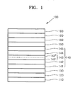
- FIG. 1 is a schematic sectional view of an organic light-emitting device (OLED) 100 according to an embodiment of the present invention.
- the OLED 100 includes a substrate 110, and a first electrode 120, a hole injection layer (HIL) 130, a hole transport layer (HTL) 140, an emission layer (EML) 150, an electron transport layer (ETL) 160, an electron injection layer (EIL) 180, and a second electrode 190 which are sequentially stacked on the substrate 110 in the stated order.
- HIL hole injection layer
- HTL hole transport layer
- EML emission layer
- ETL electron transport layer
- EIL electron injection layer
- the HTL 140 includes one hole transport unit including: a first HTL 141 having a hole transporting material; a second HTL 142 formed on the first HTL 141 and having the hole transporting material and a charge generating material; a third HTL 143 formed on the second HTL 142 and having the charge generating material; a fourth HTL 144 formed on the third HTL 143 and having the hole transporting material and the charge generating material; and a fifth HTL 145 formed on the fourth HTL 144 and having the hole transporting material.
- the substrate 110 may be any substrate that is generally used in organic light-emitting devices.
- the substrate may be a glass substrate or a transparent plastic substrate with excellent mechanical strength, thermal stability, transparency, surface smoothness, ease of handling, and waterproofness.
- the first electrode 120 is formed on the substrate 110.
- the first electrode 120 may be formed by depositing or sputtering a material used to form the first electrode 120 on the substrate 110.
- the first electrode 120 may be an anode.
- the material used to form the first electrode 120 may be a high work-function material so as to facilitate hole injection.
- the first electrode 120 may be a transmissive electrode or a semi-transmissive electrode. Transparent and conductive materials such as Indium Tim Oxide (ITO), Indium Zinc Oxide (IZO), SnO 2 , and ZnO may be used to form the first electrode 120.
- the first electrode 120 may be formed as a semi-transmissive electrode using magnesium (Mg), aluminum (Al), aluminum-lithium (Al-Li), calcium (Ca), magnesium-indium (Mg-In), magnesium-silver (Mg-Ag), or the like.
- Mg magnesium
- Al aluminum
- Al-Li aluminum-lithium
- Ca calcium
- Mg-In magnesium-indium
- Mg-Ag magnesium-silver
- the HIL 130 may be disposed on the first electrode 120.
- the HIL 130 may be formed on the first electrode 120 by vacuum deposition, spin coating, casting, Langmuir-Blodgett (LB) deposition, or the like.
- the deposition conditions may vary according to a compound that is used to form the HIL 130, and the structure and thermal properties of the HIL 130 to be formed. In general, however, conditions for vacuum deposition may include a deposition temperature of about 100 to about 500°C, a pressure of about 10 -8 to about 10 -3 torr, and a deposition rate of about 0.01 to about 100 ⁇ /sec.
- the coating conditions may vary according to a compound that is used to form the HIL 130, and the structure and thermal properties of the HIL 130 to be formed. In general, however, the coating rate may be in the range of about 2000 to about 5000 rpm, and a temperature for heat treatment which is performed to remove a solvent after coating may be in the range of about 80 to about 200°C.
- the HIL 130 may be formed of any material that is commonly used to form a HIL.
- the material that may be used to form the HIL 130 include, but are not limited to, a phthalocyanine compound such as copperphthalocyanine, 4,4',4"-tris (3-methylphenylphenylamino) triphenylamine (m-MTDATA), N,N'-di(1-naphthyl)-N,N'-diphenylbenzidine (NPB), 4,4',4"-tris(N,N-diphenylamino)triphenylamine (TDATA), 4,4',4"-tris(n-(2-naphthyl)-n-phenyl-amino)-triphenylamine(2T-NATA), polyaniline/dodecylbenzenesulfonic acid (Pani/DBSA), poly(3,4-ethylenedioxythiophene)/poly(4-styenesulfonate)
- the thickness of the HIL 130 may be in the range of about 100 to about 10,000 ⁇ , for example, about 100 to about 1000 ⁇ . When the thickness of the HIL 130 is within this range of about 100 to about 10,000 ⁇ , the HIL 130 may have excellent hole injecting ability without a substantial increase in driving voltage.
- the HTL 140 is disposed on the HIL 130.
- the HTL 140 includes the hole transport unit including: the first HTL 141 having a hole transporting material; the second HTL 142 formed on the first HTL 141 and having the hole transporting material and a charge generating material; the third HTL 143 formed on the second HTL 142 and having the charge generating material; the fourth HTL 144 formed on the third HTL 143 and having the hole transporting material and the charge generating material; and the fifth HTL 145 formed on the fourth HTL 144 and having the hole transporting material.
- the HTL 140 has a structure in which the second HTL 142, the third HTL 143, the fourth HTL 144, and the fifth HTL 145 are sequentially stacked on the first HTL 141 in the order stated, so that injection and transport of holes may be controlled and electrons may be blocked.
- the number of excitons generated in emission regions may be gradually reduced since the amount of electrons or holes may change with time during the operation of the OLED. As a result, a carrier balance may not be maintained, and thus, the lifetime of the OLED may be reduced.
- the HTL 140 has a stack structure of a plurality of layers with a similar or same energy level (the first HTL 141, the second HTL 142, the third HTL 143, the fourth HTL 144, and the fifth HTL 145), the flow of carriers may be constantly maintained while controlling migration rates of holes. Thus, lifetime characteristics of the OLED 100 may be improved.
- the hole transporting material may be represented by one selected from the group consisting of Formulae 1 and 2 below.
- R 10 is represented by -(Ar 1 ) n -Ar 5 ;
- R 16 is represented by -(Ar 11 ) m -Ar 12 ;
- Ar 1 , Ar 11 , L 1 , and L 11 are each independently selected from the group consisting of a substituted or unsubstituted C 1 -C 30 alkylene group, a substituted or unsubstituted C 2 -C 30 alkenylene group, a substituted or unsubstituted C 5 -C 30 arylene group, a substituted or unsubstituted C 4 -C 30 heteroarylene group, and -N(Q 1 )-;
- n, m, a, and b are each independently an integer from 0 to 10;
- R 1 through R 3 , R 11 through R 15 , R 17 , R 18 , R 21 through R 29 , Ar 2 , Ar 12 , and Q 1 are each independently selected from the group consisting of a hydrogen
- Ar 1 in the formula -(Ar 1 ) n -Ar 2 - for R 10 and Ar 11 in the formula -(Ar 11 ) m -Ar 12 - for R 16 include a substituted or unsubstituted C 1 -C 10 alkylene group, a substituted or unsubstituted C 2 -C 10 alkenylene group, a substituted or unsubstituted phenylene group, a substituted or unsubstituted pentalenylene group, a substituted or unsubstituted indenylene group, a substituted or unsubstituted naphthylene group, a substituted or unsubstituted azulenylene group, a substituted or unsubstituted heptalenylene group, a substituted or unsubstituted indacenylene group, a substituted or unsubstituted acenaphthylene group, a substituted or
- Q 1 may be selected from the group consisting of a hydrogen atom, a halogen atom, a hydroxyl group, a cyano group, a substituted or unsubstituted C 1 -C 10 alkyl group, a substituted or unsubstituted C 2 -C 10 alkenyl group, a substituted or unsubstituted C 2 -C 10 alkynyl group, a substituted or unsubstituted C 1 -C 10 alkoxy group, a substituted or unsubstituted C 1 -C 10 alkylthiol group, a substituted or unsubstituted C 5 -C 14 aryl group, a substituted or unsubstituted C 4 -C 14 heteroaryl group, and — N(Q 2 )(Q 3 ), but is not limited thereto.
- Ar 1 and Ar 11 may be each independently selected from the group consisting of a C 1 -C 10 alkylene group; a phenylene group; a naphthylene group; an anthrylene group; a fluorenylene group; a carbazolylene group; a pyrazolylene group; a pyridinylene group; a triazinylene group; - N(Q 1 )-; and a substituted C 1 -C 10 alkylene group, a substituted phenylene group, a substituted naphthylene group, a substituted anthrylene group, a substituted fluorenylene group, a substituted carbazolylene group, a substituted pyrazolylene group, a substituted pyridinylene group, and a substituted triazinylene group which have at least one substituent selected from the group consisting of a halogen atom, a cyano group, a hydroxyl group, a C 1 -
- Q 1 may be selected from the group consisting of a hydrogen atom; a C 1 -C 10 alkyl group; a phenyl group; a naphthyl group; a carbazolyl group; a fluorenyl group; a pyrenyl group; a substituted C 1 -C 10 alkyl group, a substituted C 1 -C 10 alkoxy group, a substituted phenyl group, a substituted naphthyl group, a substituted carbazolyl group, a substituted fluorenyl group, and a substituted pyrenyl group which have at least one substituent selected from the group consisting of a halogen atom, a cyano group, a hydroxyl group, a C 1 -C 10 alkyl group, a C 1 -C 10 alkoxy group, a phenyl group, a naphthyl group, and an anthryl group; and -N(Q 2 )
- Ar 2 in the formula -(Ar 1 ) n -Ar 2 - and Ar 12 in the formula -(Ar 11 ) m -Ar 12 - are as defined above in connection with Q 1 .
- n in the formula -(Ar 1 ) n -Ar 2 - and m in the formula -(Ar 11 ) m -Ar 12 - are each independently an integer from 0 to 10.
- n and m may be each independently 0, 1, 2, 3, 4, or 5, but are not limited thereto.
- n groups of Ar 1 in the formula -(Ar 1 ) n -Ar 2 - may be identical to or different from each other.
- the two groups of Ar 1 in -(Ar 1 ) n - may be both phenylene groups, or one of the two may be -N(Q 1 )- and the other may be a phenylene group, and various modifications may be applied thereto.
- the descriptions of -(Ar 11 ) m -Ar 12 - may be the same as those of -(Ar 1 ) n -Ar 2 -above.
- R 1 through R 3 , R 11 through R 15 , R 17 , R 18 , and R 21 through R 29 in Formulae 1 and 2 may be defined as described above in connection with Q 1 .
- R 13 may be a phenyl group, a naphthyl group, or an anthryl group, but is not limited thereto.
- R 28 and R 29 may be each independently selected from the group consisting of a hydrogen atom, a methyl group, an ethyl group, a methoxy group, an ethoxy group, a phenyl group, a naphthyl group, and an anthryl group, but are not limited thereto.
- L 1 and L 2 in Formulae 1 and 2 are defined as described above in connection with Ar 1 and Ar 11 .
- L 1 and L 2 may be each independently a phenylene group, a carbazolylene group, or a phenylcarbazolylene group, but are not limited thereto.
- a and b may be each independently an integer from 0 to 10.
- a and b may be each independently 0, 1, 2 or 3, but are not limited thereto.
- Ar 1 in the formula -(Ar 1 ) n -Ar 2 - for R 10 and Ar 11 in the formula - (Ar 11 ) m -Ar 12 - for R 16 may be each independently selected from the group consisting of a phenylene group; a carbazolylene group; a fluorenylene group; a methylfluorenylene group; a pyrazolylene group; a phenylpyrazolylene group; -N(Q 1 )-, wherein Q 1 is a hydrogen atom, a phenyl group, a fluorenyl group, a dimethylfluorenyl group, a diphenylfluorenyl group, a carbazolyl group, or a phenylcarbazolyl group; a diphenylfluorenylene group; a triazinylene group; a methyltriazinylene group; a phenyltriazinylene group;
- R 11 , R 12 , R 14 , R 15 , R 17 , R 18 , and R 21 through R 27 may be hydrogen;
- R 13 may be selected from the group consisting of a phenyl group, a naphthyl group, and an anthryl group;
- R 28 and R 29 may be each independently selected from the group consisting of a hydrogen atom, a methyl group, an ethyl group, a methoxy group, an ethoxy group, a phenyl group, a naphthyl group, and an anthryl group;
- L 11 may be a phenylene group; and
- b may be 0 or 1.
- the hole transporting material may be any one of the Compounds 1 through 37 below, but is not limited thereto.
- the charge generating material is a material that generates charge carriers (i.e., holes and/or electrons) upon exposure to light.
- the charge generating material may include a compound represented by Formula 3 below.
- R 51 to R 56 are each independently selected from the group consisting of a hydrogen atom, -CN, -SOR 100 , -SON(R 101 ) 2 , -SO 2 R 102 , -SO 2 N(R 103 ) 2 , -SO 3 R 104 , -SO 3 N(R 105 ) 2 , -NO 2 , -CFH 2 ,-CF 2 H, and -CF 3 , and R 100 to R 105 are each independently selected from the group consisting of a hydrogen atom, a substituted or unsubstituted C 1 -C 30 alkyl group, a substituted or unsubstituted C 5 -C 30 aryl group, and a substituted or unsubstituted C 4 -C 30 heteroaryl group.
- R 100 through R 105 may be each independently selected from the group consisting of a hydrogen atom, a substituted or unsubstituted C 1 -C 10 alkyl group, a substituted or unsubstituted C 5 -C 14 aryl group, and a substituted or unsubstituted C 4 -C 14 heteroaryl group.
- R 100 to R 105 may be each independently selected from the group consisting of a hydrogen atom, a methyl group, an ethyl group, a propyl group, a butyl group, a pentyl group, a methyl group substituted with at least one -CN group, an ethyl group substituted with at least one —CN group, a propyl group substituted with at least one -CN, a butyl group substituted with at least one -CN, a pentyl group substituted with at least one -CN, a phenyl group, a naphthyl group, an anthryl group, a fluorenyl group, a phenyl group substituted with at least one -CN, a naphthyl group substituted with at least one -CN, an anthryl group substituted with at least one -CN, a fluorenyl group substituted with at least one -CN, a carbazolyl group, a
- the charge generating material may be Compound 40 below, but is not limited thereto.
- the thicknesses of the first HTL 141, the third HTL 143, and the fifth HTL 145 may be each independently in the range of about 0.1 nm to about 100 nm.
- the thicknesses of the first HTL 141 and the fifth HTL 145 may be each independently in the range of about 10 nm to about 100 nm, for example, about 50 nm to about 60 nm, but are not limited thereto.
- the thickness of the third HTL 143 may be in the range of about 0.5 nm to about 100 nm, for example, about 0.5 nm to about 10 nm, but is not limited thereto.
- the thicknesses of the first HTL 141, the third HTL 143, and the fifth HTL 145 are within this range of about 0.1 nm to about 100 nm, holes may be effectively injected and transported to the EML 150 without a substantial increase in driving voltage.
- the thicknesses of the first HTL 141, the third HTL 143, and the fifth HTL 145 may be the same or different.
- the thicknesses of the second HTL 142 and the fourth HTL 144 may be each independently in the range of about 0.01 nm to about 16 nm, for example, about 0.5 nm to about 1 nm. When the thicknesses of the second HTL layer 142 and the fourth HTL 144 are within this range of about 0.01 nm to about 16 nm, holes may be effectively injected and transported to the EML 150 without a substantial increase in driving voltage.
- the thicknesses of the second HTL 142 and the fourth HTL 144 may be the same or different.
- the amount of the charge generating material contained in the second HTL 142 may be in the range of about 0.01 to about 99 parts by weight, for example, about 45 to about 55 parts by weight based on 100 parts by weight of the second HTL 142.
- the amount of the charge generating material contained in the fourth HTL 144 may be in the range of about 0.01 to about 99 parts by weight, for example, about 45 to about 55 parts by weight based on 100 parts by weight of the fourth HTL 144.
- the efficiency of OLED 100 may be improved.
- the HTL 140 may be formed by using vacuum deposition, spin coating, casting, or the like.
- the deposition and coating conditions may be similar to those for the formation of the HIL 130, though the deposition and coating conditions may vary according to the material that is used to form the HTL 140.
- the HTL 140 may be formed by preparing a first deposition source releasing the hole transporting material and a second deposition source releasing the charge generating material, disposing the first deposition source and the second deposition source to be spaced apart from each other such that a region to which the hole transporting material is released overlaps a region to which the charge generating material is released, and performing one reciprocation of the first and second deposition sources from a first end to a second end, and then from the second end to the first end of a region on which the HTL 140 will be formed on the HIL 130 in Figure 1 .
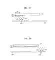
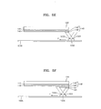
- FIGs 5A to 5G schematically illustrate a method of forming a HTL 140 on the HIL 130, according to an embodiment of the present invention.
- the substrate 110 and the first electrode 120 are disposed at one surface of the HIL 130 on which the HTL 140 is not formed, they are not shown in Figures 5A to 5G for descriptive convenience.
- a first deposition source 1001 and a second deposition source 1002 may be disposed below one surface of the HIL 130, i.e., the surface on which the substrate 110 and the first electrode 120 are not formed.
- the first deposition source 1001 may be a deposition source releasing the hole transporting material
- the second deposition source 1002 may be a deposition source releasing the charge generating material.
- a region C1 to which the hole transporting material is released by the first deposition source 1001 and a region C2 to which the charge generating material is released by the second deposition source 1002 may have a fan shape with a predetermined angle.
- the first deposition source 1001 and the second deposition source 1002 are disposed to be positioned relative to each other such that the region C1 to which the hole transporting material is released overlaps the region C2 to which the charge generating material is released. Accordingly, the hole transporting material and the charge generating material may be simultaneously deposited to form the second HTL 142 and the fourth HTL 144 including both of the hole transporting material and the charge generating material as shown in Figures 5B and 5F .
- the first deposition source 1001 and the second deposition source 1002 may be mounted on a base 1006 that is disposed on a guide rail 1005 that is disposed in a chamber and reciprocates along the guide rail 1005.
- the base 1006 may be connected to a separate drive unit (not shown) to operate.
- the base 1006 on which the first deposition source 1001 and the second deposition source 1002 are mounted to be spaced apart from each other by a predetermined distance may move in the B direction from a first end A below the HIL 130 when the first deposition source 1001 and the second deposition source 1002 are in an "on" state as shown in Figure 5A .
- only the hole transporting material is deposited on the HIL 130 to form the first HTL 141 including the hole transporting material (D1).
- the first HTL 141 is continuously deposited toward a second end E below the HIL 130 as the base 1006 moves in the B direction.
- a region (D2) on which the hole transporting material and the charge generating material are simultaneously deposited is formed to form the second HTL 142, including the hole transporting material and the charge generating material, on the first HTL 141 as shown in Figure 5B .
- the second HTL 142 is continuously deposited toward the second end E with respect to the second end E (See Figure 5D ) as the base 1006 moves in the B direction.
- a first charge generating material-containing layer 143' (D3) is formed on the second HTL 142 as shown in Figure 5C .
- the first HTL 141 including the hole transporting material, the second HTL 142 including the hole transporting material and the charge generating material, and the first charge generating material-containing layer 143' are formed on the HIL 130 as shown in Figure 5D .
- a second charge generating material-containing layer 143" is first formed as shown in Figure 5E .
- the fourth HTL 144 including the hole transporting material and the charge generating material and the fifth HTL 145 including the charge generating material are sequentially formed on the second charge generating material-containing layer 143" as shown in Figure 5F
- the first charge generating material-containing layer 143' and the second charge generating material-containing layer 143" have the same component, i.e., the charge generating material
- the interface between the first charge generating material-containing layer 143' and the second charge generating material-containing layer 143" may not be clearly distinguished, so that they may be seen as a single layer, i.e., the third HTL 143 including the charge generating material.
- the interface between the first charge generating material-containing layer 143' and the second charge generating material-containing layer 143" is shown as a dash line instead of a solid line in Figure 5F .
- the first HTL 141 including the hole transporting material, the second HTL 142 including the hole transporting material and the charge generating material, the third HTL 143 including the charge generating material, the fourth HTL 144 including the hole transporting material and the charge generating material, and the fifth HTL 145 including the hole transporting material may be sequentially formed on the HIL 130 as shown in Figure 5G .
- the third HTL 143 includes two charge generating material-containing layers, i.e., the first charge generating material-containing layer 143' and the second charge generating material-containing layer 143", an interface S' between the first charge generating material-containing layer 143' and the second charge generating material-containing layer 143" is not clearly distinguished, so that they may be seen as a single layer.
- the interface S' is shown as a dash line in Figure 5G .
- the HTL 140 including one hole transport unit having the first HTL 141, the second HTL 142, the third HTL 143, the fourth HTL 144, and the fifth HTL 145 may be prepared by one reciprocation of the base 1006 on which the first deposition source 1001 and the second deposition source 1002 are mounted from the first end A to the second end E, and then from the second end E to the first end A.
- one hole transport unit may be formed using the method of forming the layers shown in Figure 5A to 5G .
- the stacking process is simply and quickly performed, and a plurality of layers may be simultaneously deposited in a single chamber without evacuating the chamber between the formations of the layers.
- the EML 150 may be formed on the HTL 140 by vacuum deposition, spin coating, casting, LB deposition, or the like.
- the conditions for deposition and coating are similar to those for the formation of the HIL 130, although the conditions for deposition and coating may vary according to the material that is used to form the EML 150.
- the EML 150 may be formed of a compound, or a combination of a host and a dopant.
- the host include, but are not limited to, Alq 3 , 4,4'-N,N'- dicarbazole-biphenyl (CBP), poly(n-vinylcarbazole) (PVK), 9,10-di(naphthalene-2-yl)anthracene (ADN), 4,4',4"-tris(N-carbazolyl)- triphenylamine (TCTA), 1,3,5-tris(N-phenylbenzimidazole-2-yl)benzene (TPBI), 3-tert-butyl-9,10-di-2-naphthylanthracene (TBADN), E3, distyrylarylene (DSA), bis(2-(2-hydroxyphenyl)benzothiazolate)zinc (Zn(BTZ) 2 ), Compound 51 below, and Compound 52 below.
- CBP 4,4
- red dopants examples include PtOEP, Ir(piq) 3 , and Btp 2 Ir(acac), but are not limited thereto.
- examples of known blue dopants include F 2 Irpic, (F 2 ppy) 2 Ir(tmd), Ir(dfppz) 3 , ter-fluorene, 4,4'-bis(4-diphenyl aminostyyl)biphenyl (DPAVBi), 2,5,8,11-tetra-tert-butyl perylene (TBPe), Compound 54 below, and 4,4'-bis(2,2-diphenylethenyl)biphenyl (DPVBi).
- the amount of the dopant may be in the range of about 0.01 to about 15 parts by weight based on 100 parts by weight of the host, but is not limited thereto.
- the thickness of the EML 150 may be in the range of about 100 to about 1,000 ⁇ , for example, about 200 to about 600 ⁇ . When the thickness of the EML 150 is within this range of about 100 to about 1,0001 ⁇ , the EML 150 may have excellent light emitting ability without a substantial increase in driving voltage.
- a hole blocking layer (not shown in Figure 1 ) may be formed on the EML 150 by using vacuum deposition, spin coating, casting, LB deposition, or the like, in order to prevent diffusion of triplet excitons or holes into an ETL 160.
- the HBL is formed using vacuum deposition or spin coating, the conditions for deposition and coating may be similar to those for the formation of the HIL 130, although the conditions for deposition and coating may vary according to the material that is used to form the HBL. Any material that is commonly used to form a HBL may be used. Examples of materials for forming the HBL include an oxadiazole derivative, a triazole derivative, and a phenanthroline derivative, but are not limited thereto.
- the thickness of the HBL may be in a range of about 50 to about 1,000 ⁇ , for example, about 100 to about 3001 ⁇ . When the thickness of the HBL is within this range of about 50 to about 1,000 ⁇ , the HBL may have excellent hole blocking ability without a substantial increase in driving voltage.
- the ETL 160 is formed on the EML 150 or on the HBL if the HBL is formed.
- the ETL 160 includes an electron transporting material and a metal-containing material.
- the electron transporting material may be any electron transporting material.
- the electron transporting material may be selected from the group consisting of Compound 60 and compounds represented by Formulae 4, and 5 below.
- R 61 to R 66 are each independently a hydrogen atom, a halogen atom, a hydroxyl group, a cyano group, a substituted or unsubstituted C 1 -C 30 alkyl group, a substituted of unsubstituted C 1 -C 30 alkoxy group, a substituted or unsubstituted C 1 -C 30 acyl group, a substituted or unsubstituted C 2 -C 30 alkenyl group, a substituted or unsubstituted C 2 -C 30 alkynyl group, a substituted or unsubstituted C 6 -C 30 aryl group, or a substituted or unsubstituted C 3 -C 30 heteroaryl group, wherein at least two adjacent groups of R 61 to R 66 are optionally bonded to each other to form a saturated or unsaturated ring;
- L 21 is a substituted or unsubstituted C 1 -C 30 alkylene group, a substituted or unsubstituted C 6 -C 30 arylene group, or a substituted or unsubstituted C 3 -C 30 heteroarylene group;
- Q 11 through Q 19 are, each independently, a hydrogen atom, a substituted or unsubstituted C 6 -C 30 aryl group, or a substituted or unsubstituted C 3 -C 31 heteroaryl group;
- c is an integer from 0 to 10.
- R 61 to R 66 may be each independently selected from the group consisting of a hydrogen atom, a halogen atom, a hydroxyl group, a cyano group, a methyl group, an ethyl group, a propyl group, a butyl group, a methoxy group, an ethoxy group, a propoxy group, a butoxy group, a phenyl group, a naphthyl group, an anthryl group, a pyridinyl group, and a pyrazinyl group, but are not limited thereto.
- R 61 to R 64 may be hydrogen atoms
- R 65 may be selected from the group consisting of a halogen atom, a hydroxyl group, a cyano group, a methyl group, an ethyl group, a propyl group, a butyl group, a methoxy group, an ethoxy group, a propoxy group, a butoxy group, a phenyl group, a naphthyl group, an anthryl group, a pyridinyl group, and a pyrazinyl group.
- R 61 to R 66 may be hydrogen atoms, but are not limited thereto.
- Q 11 and Q 19 may be each independently selected from the group consisting of a hydrogen atom, a phenyl group, a naphthyl group, an anthryl group, a pyridinyl group, and a pyrazinyl group, but are not limited thereto.
- Q 11 , Q 13 through Q 16 , Q 18 , and Q 19 may be hydrogen atoms
- Q 12 and Q 17 may be each independently selected from the group consisting of a phenyl group, a naphthyl group, an anthryl group, a pyridinyl group, and a pyrazinyl group, but are not limited thereto.
- L 21 may be selected from the group consisting of a phenylene group, a naphthylene group, an anthrylene group, a pyridinylene group, and a pyrazinylene group, but is not limited thereto.
- L 21 may be a phenylene group or a pyridinylene group.
- c may be 1, 2, or 3, but is not limited thereto.
- the electron transport material may be Compound 60 shown above or Compound 61 or 62 below.
- the metal-containing material may inject electrons and block holes.
- the metal-containing material may be a Li complex.
- the metal-containing material may be lithium quinolate (LiQ) or Compound 81 below, but is not limited thereto.
- the thickness of the ETL 160 may be in the range of about 50 to about 1,000 ⁇ , for example, about 100 to about 300 ⁇ . When the thickness of the ETL 160 is within the range of about 50 to about 1,000 ⁇ , an excellent electron transporting ability of the ETL 160 may be obtained without a substantial increase in driving voltage.
- the EIL 180 which facilitates injection of electrons from the cathode (second electrode 190), may be formed on the ETL 160.
- Examples of materials for forming the EIL 180 include LiF, NaCl, CsF, Li 2 O, and BaO, which are known in the art.
- Deposition and coating conditions for forming the EIL 180 are similar to those for the formation of the HIL 130, although the deposition and coating conditions may vary according to a material that is used to form the EIL 180.
- the thickness of the EIL 180 may be in the range of about 1 to about 100 ⁇ , for example, about 5 to about 90 ⁇ . When the thickness of the EIL 180 is within this range of about 1 to about 100 ⁇ , the EIL 180 may have satisfactory electron injecting ability without a substantial increase in driving voltage.
- the second electrode 190 is disposed on the EIL 180.
- the second electrode 190 may be a cathode, which is an electron injecting electrode.
- a metal for forming the second electrode 190 may be a metal, an alloy, an electrically conductive compound, which have a low-work function, or a mixture thereof.
- the second electrode 190 may be a reflective electrode formed of lithium (Li), magnesium (Mg), aluminum (A1), aluminum-lithium, calcium (Ca), magnesium (Mg)-indium (In), magnesium (Mg)-silver (Ag), or the like.
- the second electrode 190 may be a transmissive or semi-transmissive electrode formed of a transparent conductive material such as ITO and IZO.
- the HTL 140 of the OLED 100 has a multi-layered structure, in which energy levels of the layers are similar to each other, and the ETL 160 includes the electron transporting material and the metal-containing material.
- the balance in the flow of holes and electrons is maintained for a long period of time, the injection and transport of electrons are adjusted, and holes are blocked, so that the OLED 100 may have long lifetime.
- Figure 2 is a schematic cross-sectional view of an OLED 200 according to an embodiment of the present invention.
- the OLED 200 includes a substrate 210, and a first electrode 220, a HIL 230, a HTL 240, an EML 250, an ETL 260, an EIL 280, and a second electrode 290 which are sequentially stacked on the first electrode 220 in the order stated.
- the HTL 240 include two hole transport units, i.e., a first hole transport unit 240a and a second hole transport unit 240b.
- the HTL 240 includes: the first hole transport unit 240a including a first HTL 241 having a hole transporting material; a second HTL 242 formed on the first HTL 241 and having the hole transporting material and a charge generating material; a third HTL 243 formed on the second HTL 242 and having the charge generating material; a fourth HTL 244 formed on the third HTL 243 and having the hole transporting material and the charge generating material; and a fifth HTL 245 formed on the fourth HTL 244 and having the hole transporting material; and the second hole transport unit 240b including a sixth HTL 246 formed on the fifth HTL 245 and having the hole transporting material; a seventh HTL 247 formed on the sixth HTL 246 and having the hole transporting material and the charge generating material; an eighth HTL 248 formed on the seventh HTL 247 and having
- the method of forming the layers described with reference to Figures 5A to 5G may be repeated twice to prepare the HTL 240.
- the base 1006 on which the first deposition source 1001 and the second deposition source 1002 are mounted is reciprocated twice along the guide rail 1005.
- the HTL 240 may be formed by the following process: start from the first end A ⁇ move in the B direction ⁇ arrive at the second end E ⁇ move in the F direction ⁇ arrive at the first end A ⁇ move in the B direction ⁇ arrive at the second end E ⁇ move in the F direction ⁇ arrive at the first end A.
- the third HTL 243 includes two charge generating material-containing layers, i.e., a first charge generating material-containing layer 243' and a second charge generating material-containing layer 243", and components of the two layers are the same as the charge generating material.
- the interface between the first charge generating material-containing layer 243' and the second charge generating material-containing layer 243" is not clearly distinguished, so that the third HTL 243 may be seen as a single layer.
- the eighth HTL 248 includes two charge generating material-containing layers, i.e., a first charge generating material-containing layer 248' and a second charge generating material-containing layer 248", and components of the two layers are the same as the charge generating material.
- the interface between the first charge generating material-containing layer 248' and the second charge generating material-containing layer 248" is not clearly distinguished, so that the eighth HTL 248 may be seen as a single layer.
- the interface between the first charge generating material-containing layer 243' and the second charge generating material-containing layer 243" of the third HTL 243 and the interface between the first charge generating material-containing layer 248' and the second charge generating material-containing layer 248" of the eighth HTL 248 are shown as a dash line instead of a solid line in Figure 2 .
- the interface between the fifth HTL 245 and the sixth HTL 246 is shown as a dash line in Figure 2 . Since the component of the fifth HTL 245 (hole transporting material) formed after the first reciprocation of the base 1006 (start from the first end A ⁇ move in the B direction ⁇ arrive at the second end E ⁇ move in the F direction ⁇ arrive at the first end A) is the same as the component of the sixth HTL 246 (hole transporting material) formed by the second reciprocation of the base 1006 that starts from the first end A after the first reciprocation, the interface between the fifth HTL 245 and the sixth HTL 246 is not clearly distinguished, and thus the fifth HTL 245 and the sixth HTL 246 may be seen as a single layer.
- the OLED 200 of Figure 2 has the same structure as the OLED 100 of Figure 1 , except that the OLED 200 includes the HTL 240 having two hole transport units instead of one hole transport unit, and thus the material used to form each layer and the thickness of each layer of the OLED 200 are defined as described above with reference to Figure 1 .
- Figure 3 is a schematic cross-sectional view of an OLED 300 according to an embodiment of the present invention.
- the OLED 300 includes a substrate 310, and a first electrode 320, a HIL 330, a HTL 340, an EML 350, an ETL 360, an EIL 380, and a second electrode 390 which are sequentially stacked on the substrate 310 in the order stated.
- the HTL 340 include two hole transport units, i.e., a first hole transport unit 340a and a second hole transport unit 340b.
- the HTL 340 includes: the first hole transport unit 340a including a first HTL 341 having a hole transporting material; a second HTL 342 formed on the first HTL 341 and having the hole transporting material and a charge generating material; a third HTL 343 formed on the second HTL 342 and having the charge generating material; a fourth HTL 344 formed on the third HTL 343 and having the hole transporting material and the charge generating material; and a fifth HTL 345 formed on the fourth HTL 344 and having the hole transporting material; and the second hole transport unit 340b including a sixth HTL 346 formed on the fifth HTL 345 and having a hole transporting material; a seventh HTL 347 formed on the sixth HTL 346 and having the hole transporting material and the charge generating material; an eighth HTL 348 formed on the seventh HTL 347 and
- the HTL 340 is defined as the HTL 240 described above.
- the ETL 360 includes one electron transport unit including: a first ETL 361 having an electron transporting material; a second ETL 362 formed on the first ETL 361 and having the electron transporting material and the metal-containing material; a third ETL 363 formed on the second ETL 362 and having the metal-containing material; a fourth ETL 364 formed on the third ETL 363 and having the electron transporting material and the metal-containing material; and a fifth ETL 365 formed on the fourth ETL 364 and having the electron transporting material.
- the ETL 360 has a structure in which the second ETL 362, the third ETL 363, the fourth ETL 364, and the fifth ETL 365 are sequentially stacked on the first ETL 361 in the order stated, so that injection and transport of electrons may be controlled and holes may be blocked.
- the number of excitons generated in emission regions may be gradually reduced since the amount of electrons or holes may change with time during the operation of the OLED. As a result, a carrier balance may not be maintained, and thus, the lifetime of an OLED may be reduced.
- the ETL 360 has a stack structure of a plurality of layers with a similar or same energy level (the first ETL 361, the second ETL 362, the third ETL 363, the fourth ETL 364, and the fifth ETL 365), the flow of carriers may be constantly maintained while controlling migration rates of electrons. Thus, lifetime characteristics of the OLED 300 may be improved.
- the ETL 360 may be formed by preparing a third deposition source releasing the electron transporting material and a fourth deposition source releasing the metal-containing material, disposing the third deposition source and the fourth deposition source to be spaced apart from each other such that a region to which the electron transporting material is released overlaps a region to which the metal-containing material is released, and performing one reciprocation of the third and fourth deposition sources from a first end to a second end, and then from the second end to the first end of a region on which the ETL 360 will be formed (on the EML 350).
- the method of forming the ETL 360 may be easily understood by the descriptions above with reference to Figures 5A to 5G , in which the hole transporting material is replaced with the electron transporting material, the charge generating material is replaced with the metal-containing material, the first deposition source is replaced with the third deposition source, and the second deposition source is replaced with the fourth deposition source.
- a first metal-containing material-containing layer 363' and a second metal-containing material-containing layer 363" have the same component, i.e., the metal-containing material, therefore the interface between the first metal-containing material-containing layer 363' and the second metal-containing material-containing layer 363" may not be clearly distinguished, so that they may be seen as a single layer, i.e., the third ETL 363 including the metal-containing material.
- the interface between the first metal-containing material-containing layer 363' and the second metal-containing material-containing layer 363" is shown as a dash line instead of a solid line in Figure 3 .
- the thicknesses of the first ETL 361, the third ETL 363, and the fifth ETL 365 may be each independently in the range of about 0.01 nm to about 1 nm, for example, about 0.5 nm to about 0.7 nm. When the thicknesses of the first ETL 361, the third ETL 363, and the fifth ETL 365 are within this range of about 0.01 nm to about 1 nm, electrons may effectively be injected and transported to the EML 350 without a substantial increase in driving voltage.
- the thicknesses of the first ETL 361, the third ETL 363, and the fifth ETL 365 may be the same or different.
- the thicknesses of the second ETL 362 and the fourth ETL 364 may be each independently a thickness in the range of about 6 nm to about 16 nm, for example, about 6 nm to about 10 nm. When the thicknesses of the second ETL layer 362 and the fourth ETL 364 are within this range of about 6 nm to about 16 nm, electrons may effectively be injected and transported to the EML 350 without a substantial increase in driving voltage.
- the thicknesses of the second ETL 362 and the fourth ETL 364 may be the same or different.
- the amount of the metal-containing material contained in the second ETL 362 may be in the range of about 20 to about 80 parts by weight, for example, about 45 to about 55 parts by weight based on 100 parts by weight of the second ETL 362.
- the amount of the metal-containing material contained in the fourth ETL 364 may be in the range of about 20 to about 80 parts by weight, for example, about 45 to about 55 parts by weight based on 100 parts by weight of the fourth ETL 364.
- the efficiency of OLED 300 may be improved.
- the electron transporting material and the metal-containing material of the ETL 360 are defined as described above with reference to Figure 1 .
- the OLED 300 of Figure 3 has the same structure as the OLED 200 of Figure 2 , except that the OLED 300 includes the ETL 360 having a multi-layered structure, and thus the material used to form each layer and the thickness of each layer of the OLED 300 are defined as described above with reference to Figures 1 and 2 .
- Figure 4 is a schematic cross-sectional view of an OLED 400 according to an embodiment of the present invention.
- the OLED 400 includes a substrate 410, and a first electrode 420, a HIL 430, a HTL 440, an EML 450, an ETL 460, an EIL 480, and a second electrode 490 which are sequentially stacked on the substrate 410 in the order stated.
- the HTL 440 include two hole transport units, i.e., a first hole transport unit 440a and a second hole transport unit 440b.
- the HTL 440 includes: the first hole transport unit 440a including a first HTL 441 having a hole transporting material; a second HTL 442 formed on the first HTL 441 and having the hole transporting material and a charge generating material; a third HTL 443 formed on the second HTL 442 and having the charge generating material; a fourth HTL 444 formed on the third HTL 443 and having the hole transporting material and the charge generating material; and a fifth HTL 445 formed on the fourth HTL 444 and having the hole transporting material; and the second hole transport unit 440b including a sixth HTL 446 formed on the fifth HTL 445 and having a hole transporting material; a seventh HTL 447 formed on the sixth HTL 446 and having the hole transporting material and the charge generating material; an eighth HTL 448 formed on the seventh HTL 447 and
- the HTL 440 is defined as the HTL 240 described above.
- the ETL 460 includes two electron transport units, i.e., a first electron transport unit 460a and a second electron transport unit 440b.
- the ETL 460 includes: the first electron transport unit 460a including a first ETL 461 having an electron transporting material; a second ETL 462 formed on the first ETL 461 and having the electron transporting material and the metal-containing material; a third ETL 463 formed on the second ETL 462 and having the metal-containing material; a fourth ETL 464 formed on the third ETL 463 and having the electron transporting material and the metal-containing material; and a fifth ETL 465 formed on the fourth ETL 464 and having the electron transporting material; and the second electron transport unit 460b including a sixth ETL 466 formed on the fifth ETL 465 and having the electron transporting material; a seventh ETL 467 formed on the sixth ETL 466 and having the electron transporting material and the metal-containing material; a eighth ETL 468 formed on the seventh ETL 467 and having the
- the method of forming the layers described with reference to Figures 5A to 5G may be repeated twice to prepare the ETL 460 and replacing the hole transporting material with the electron transporting material, replacing the charge generating material with the metal-containing material, replacing the first deposition source with the third deposition source, and replacing the second deposition source with the fourth deposition source.
- the third ETL 463 includes two metal-containing material-containing layers, i.e., a first metal-containing material-containing layer 463' and a second metal-containing material-containing layer 463", and components of the two layers are the same.
- the interface between the first metal-containing material-containing layer 463' and the second metal-containing material-containing layer 463" is not clearly distinguished, so that the third ETL 463 may be seen as a single layer.
- the eighth ETL 468 may be seen as a single layer.
- the interface between the fifth ETL 465 and the sixth ETL 466 is shown as a dash line in Figure 4 . Since the component of the fifth ETL 465 (electron transporting material) formed after the first reciprocation of the base 1006 (start from the first end A ⁇ move in the B direction ⁇ arrive at the second end E ⁇ move in the F direction ⁇ arrive at the first end A) is the same as the component of the sixth ETL 466 (electron transporting material) formed by the second reciprocation of the base 1006 that starts from the first end A after the first reciprocation, the interface between the fifth ETL 465 and the sixth ETL 466 is not clearly distinguished, and thus the fifth ETL 465 and the sixth ETL 466 may be seen as a single layer.
- the OLED 400 of Figure 4 has the same structure as the OLED 300 of Figure 3 , except that the OLED 400 includes the ETL 460 having two electron transport units instead of one electron transport unit, and thus the material used to form each layer and the thickness of each layer of the OLED 400 are defined as described above with reference to Figures 1 , 2 , and 3 .
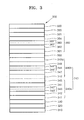
- FIG. 6 is a schematic sectional view of an OLED 10 according to an embodiment of the present invention.
- the OLED 10 according to an embodiment of the present invention includes a substrate 11, and a first electrode 12, a HIL 13, a HTL 14, an EML 15, an ETL 16, an EIL 18, and a second electrode 19 which are sequentially stacked on the substrate 11 in the order stated.
- the HTL 14 includes one hole transport unit including: a first HTL 14a having a hole transporting material; a third HTL 14b formed on the first HTL 14a and having a charge generating material; and a fifth HTL 14c formed on the third HTL 14b and having the hole transporting material.
- the substrate 11, the first electrode 12, the HIL 13, the EML 15, the ETL 16, the EIL 18, and the second electrode 19 are defined as described above with reference to Figure 1 .
- the HTL 14 includes the first HTL 14a, the third HTL 14b, and the fifth HTL 14c which are defined as described above with reference to first HTL 141, the third HTL 143, and the fifth HTL 145 of Figure 1 . That is, the OLED 10 of Figure 6 has the same structure as the OLED 100 of Figure 1 , except that the OLED 10 does not include the second HTL 142 and the fourth HTL 144 of Figure 1 .
- the third HTL 14b of the OLED 10 may include the charge generating material as described above.
- the third HTL 14b may include a first charge generating material-containing layer 14b' and a second charge generating material-containing layer 14b".
- the interface S' between the first charge generating material-containing layer 14b' and the second charge generating material-containing layer 14b" is not clearly distinguished, so that they may be seen as a single layer, i.e., the third HTL 14b including the charge generating material.
- the interface between the first charge generating material-containing layer 14b' and the second charge generating material-containing layer 14b" is shown as a dash line instead of a solid line in Figure 5F .
- the HTL 14 has a structure in which the first HTL 14a, the third HTL 14b, and the fifth HTL 14c are sequentially stacked, so that injection and transport of holes may be controlled and electrons may be blocked. Accordingly, lifetime characteristics of the OLED 10 may be improved.
- the HTL 14 of the OLED 10 may be formed by preparing the base 1006 on which the first deposition source 1001 and the second deposition source 1002 are mounted, as shown in Figure 5A , disposing a anti-deposition plate between the first deposition source 1001 and the second deposition source 1002, and reciprocating the base 1006 once according to the following process: start from the first end A ⁇ move in the B direction ⁇ arrive at the second end E ⁇ move in the F direction ⁇ arrive at the first end A.
- the anti-deposition plate is disposed between the first deposition source 1001 and the second deposition source 1002, the simultaneous deposition of the hole transporting material released from the first deposition source 1001 and the charge generating material released from the second deposition source 1002 is substantially prevented, and thus the first HTL 14a, the third HTL 14b, and the fifth HTL 14c may be sequentially stacked.
- the OLED and the method of manufacturing the OLED according to an embodiment of the present invention are described with reference to Figures 1 , 2 , 3 , 4 , 5a to 5g, and 6 , but are not limited thereto, and various modifications may be applied thereto.
- the HTL of the OLED according to an embodiment may include three or more hole transport units and/or the ETL of the OLED may include three or more electron transport units, and various modifications may be applied thereto.
- the HTL may be formed on the first electrode without forming the HIL, and various modifications may be applied thereto.
- the HTL and the ETL described above may also be combined with each other.
- an OLED including the HTL 14 of the OLED 10 shown in Figure 6 and the ETL 360 of the OLED 300 shown in Figure 3 may also be manufactured.
- a sealing layer may further be formed on the second electrode in order to seal the OLED, and various modifications may be applied thereto.
- a glass substrate including a 15 ⁇ /cm 2 (70 ⁇ ) ITO (a first electrode) (available from Corning Co.) was cut to a size of 50 mm x 50 mm x 0.5 mm, ultrasonically washed with isopropyl alcohol for 5 minutes and then with pure water for 5 minutes, heat-treated for 30 minutes, and treated with N 2 plasma.
- a HTL was formed on the ITO electrode using Compound 14 as a hole injecting and transporting material and Compound 40 as a charge generating material by using the method described with reference to Figures 5A to 5G , by which the first deposition source 1001 emits Compound 14 and the second deposition source 1002 emits Compound 40 while the base 1006 reciprocates once (start from the first end A ⁇ move in the B direction ⁇ arrive at the second end E ⁇ move in the F direction ⁇ arrive at the first end A).
- a HTL including one hole transport unit including a first HTL formed of Compound 14 and having a thickness of 6001 ⁇ , a second HTL formed of Compound 14 and Compound 40 and having a thickness of 10 ⁇ , a third HTL formed of Compound 40 and having a thickness of 301 ⁇ , a fourth HTL formed of Compound 14 and Compound 40 and having a thickness of 10 ⁇ , and a fifth HTL formed of Compound 14 and having a thickness of 6001 ⁇ was prepared.
- 97 wt% of Alq 3 as a host and 3 wt% of DPVBI as a dopant were deposited on the HTL to form an EML having a thickness of 200 ⁇ .
- Compound 62 and LiQ were co-deposited on the EML to form an ETL having a thickness of 300 ⁇ , wherein the amount of LiQ was 50 parts by weight based on 100 parts by weight of the ETL, and LiF was vacuum-deposited on the ETL to form an EIL having a thickness of 5 ⁇ . Then, Mg and Ag were vacuum-deposited on the EIL to form a second electrode having a thickness of 120 ⁇ , and Alq 3 was vacuum-deposited on the second electrode to form an organic capping layer, thereby completing the manufacture of an OLED.
- Figure 7 is a graph illustrating time-brightness of the OLED of Example 1.
- the Y-axis indicates brightness (%). When the time is zero (0), the brightness is 100%. The brightness was evaluated using a PR650 (Spectroscan) Source Measurement Unit. (PhotoResearch).
- Figure 8 is a graph illustrating voltage-current density of the OLED of Example 1. In Figure 8 , the X-axis indicates voltage (V), and the Y-axis indicates current density (mA/cm 2 ). Referring to Figures 7 and 8 , the OLED manufactured according to Example 1 has excellent electrical and lifetime characteristics.
Landscapes
- Physics & Mathematics (AREA)
- Spectroscopy & Molecular Physics (AREA)
- Chemical & Material Sciences (AREA)
- Engineering & Computer Science (AREA)
- Materials Engineering (AREA)
- Optics & Photonics (AREA)
- Electroluminescent Light Sources (AREA)
- Nitrogen Condensed Heterocyclic Rings (AREA)
- Plural Heterocyclic Compounds (AREA)
- Indole Compounds (AREA)
Applications Claiming Priority (1)
| Application Number | Priority Date | Filing Date | Title |
|---|---|---|---|
| KR1020100020402A KR101097339B1 (ko) | 2010-03-08 | 2010-03-08 | 유기 발광 소자 및 이의 제조 방법 |
Publications (3)
| Publication Number | Publication Date |
|---|---|
| EP2365555A2 true EP2365555A2 (fr) | 2011-09-14 |
| EP2365555A3 EP2365555A3 (en) | 2012-06-06 |
| EP2365555B1 EP2365555B1 (fr) | 2017-11-15 |
Family
ID=43795135
Family Applications (1)
| Application Number | Title | Priority Date | Filing Date |
|---|---|---|---|
| EP11157291.3A Active EP2365555B1 (fr) | 2010-03-08 | 2011-03-08 | Dispositif électroluminescent organique et son procédé de fabrication |
Country Status (5)
| Country | Link |
|---|---|
| US (1) | US9472767B2 (fr) |
| EP (1) | EP2365555B1 (fr) |
| JP (2) | JP2011187959A (fr) |
| KR (1) | KR101097339B1 (fr) |
| CN (1) | CN102201432B (fr) |
Cited By (9)
| Publication number | Priority date | Publication date | Assignee | Title |
|---|---|---|---|---|
| WO2013060418A1 (fr) * | 2011-10-27 | 2013-05-02 | Merck Patent Gmbh | Matériaux pour dispositifs électroniques |
| EP3029752A3 (fr) * | 2014-12-02 | 2016-06-15 | Samsung Display Co., Ltd. | Dispositif électroluminescent organique |
| EP3051604A1 (fr) * | 2015-01-30 | 2016-08-03 | Samsung Display Co., Ltd. | Dispositif électroluminescent organique |
| EP3243812A3 (fr) * | 2016-05-09 | 2018-01-10 | Samsung Display Co., Ltd. | Composé polycyclique et dispositif électroluminescent organique l'incluant |
| US9917272B2 (en) | 2012-10-09 | 2018-03-13 | Merck Patent Gmbh | Electronic device |
| EP3460864A1 (fr) * | 2012-03-15 | 2019-03-27 | Merck Patent GmbH | Dispositifs électroniques |
| TWI700275B (zh) * | 2015-01-30 | 2020-08-01 | 南韓商三星顯示器有限公司 | 有機發光裝置 |
| EP3742511A1 (fr) * | 2019-05-07 | 2020-11-25 | Canon Kabushiki Kaisha | Dispositif électroluminescent organique et appareil d'affichage, appareil de conversion photoélectrique, appareil électronique, appareil d'éclairage et objet mobile le comprenant |
| US12232417B2 (en) | 2017-12-29 | 2025-02-18 | Lg Display Co., Ltd. | Organic light emitting device and organic light emitting display |
Families Citing this family (68)
| Publication number | Priority date | Publication date | Assignee | Title |
|---|---|---|---|---|
| KR101881081B1 (ko) * | 2011-06-22 | 2018-08-20 | 삼성디스플레이 주식회사 | 헤테로고리 화합물, 이를 포함하는 유기 발광 소자 및 평판 표시 장치 |
| EP2750214B1 (fr) * | 2011-10-05 | 2020-06-17 | LG Chem, Ltd. | Dispositif électroluminescent organique et son procédé de fabrication |
| KR101305869B1 (ko) * | 2011-10-12 | 2013-09-09 | 포항공과대학교 산학협력단 | 단순화된 유기 발광 소자 및 이의 제조 방법 |
| CN102643296B (zh) * | 2011-10-20 | 2014-12-24 | 京东方科技集团股份有限公司 | 一种甲酸锂金属络合物及其制作方法、有机电致发光器件 |
| KR20130050713A (ko) | 2011-11-08 | 2013-05-16 | 삼성디스플레이 주식회사 | 유기 발광 소자, 이의 제조 방법 및 이를 포함하는 평판 표시 장치 |
| KR101927943B1 (ko) * | 2011-12-02 | 2018-12-12 | 삼성디스플레이 주식회사 | 다층 구조의 정공수송층을 포함하는 유기 발광 소자 및 이를 포함하는 평판 표시 장치 |
| KR101429924B1 (ko) * | 2011-12-08 | 2014-08-14 | 엘지디스플레이 주식회사 | 탠덤형 백색 유기 발광 소자 |
| KR101927941B1 (ko) * | 2011-12-19 | 2018-12-12 | 삼성디스플레이 주식회사 | 다층 구조의 정공수송층을 포함하는 유기 발광 소자 및 이를 포함하는 평판 표시 장치 |
| JP6118034B2 (ja) | 2012-02-06 | 2017-04-19 | ユー・ディー・シー アイルランド リミテッド | 有機電界発光素子とそれに用いることができる化合物および有機電界発光素子用材料、並びに該素子を用いた発光装置、表示装置及び照明装置 |
| WO2013118846A1 (fr) | 2012-02-10 | 2013-08-15 | 出光興産株式会社 | Dérivé d'amine aromatique, élément électroluminescent organique et dispositif électronique |
| KR101973166B1 (ko) * | 2012-03-27 | 2019-04-29 | 삼성디스플레이 주식회사 | 유기 발광 소자 및 이를 포함하는 유기 발광 표시 장치 |
| CN102694131B (zh) * | 2012-06-04 | 2015-06-03 | 京东方科技集团股份有限公司 | 一种有机电致发光器件及其制备方法以及显示装置 |
| KR101932563B1 (ko) * | 2012-06-27 | 2018-12-28 | 삼성디스플레이 주식회사 | 다층 구조의 정공수송층을 포함하는 유기 발광 소자 및 이를 포함하는 유기 발광 표시 장치 |
| CN104662010B (zh) * | 2012-08-30 | 2017-08-25 | 出光兴产株式会社 | 芳香族胺衍生物以及使用其的有机电致发光元件 |
| KR101974757B1 (ko) | 2012-08-31 | 2019-05-02 | 이데미쓰 고산 가부시키가이샤 | 방향족 아민 유도체 및 이것을 이용한 유기 전기발광 소자 |
| WO2014034791A1 (fr) * | 2012-08-31 | 2014-03-06 | 出光興産株式会社 | Élément électroluminescent organique |
| KR102017745B1 (ko) * | 2012-10-12 | 2019-09-04 | 삼성디스플레이 주식회사 | 유기 발광 소자, 이의 제조 방법 및 이를 포함하는 유기 발광 표시 장치 |
| KR102014168B1 (ko) * | 2012-10-12 | 2019-08-27 | 삼성디스플레이 주식회사 | 유기 발광 소자, 이의 제조 방법 및 물질층 형성 방법 |
| KR102081119B1 (ko) * | 2012-10-31 | 2020-02-25 | 엘지디스플레이 주식회사 | 유기 발광 소자 및 이를 이용한 유기 발광 표시 장치 |
| GB2508289B (en) * | 2012-10-31 | 2015-09-30 | Lg Display Co Ltd | Organic light emitting display device |
| GB2508092B (en) * | 2012-10-31 | 2015-09-23 | Lg Display Co Ltd | Light emitting device and organic light emitting display device including the same |
| CN102931355B (zh) * | 2012-11-09 | 2015-12-09 | 四川虹视显示技术有限公司 | Oled器件 |
| CN103204798B (zh) * | 2012-11-12 | 2015-08-26 | 吉林奥来德光电材料股份有限公司 | 一种芳香胺衍生物、其制备方法以及由其制成的有机电致发光器件 |
| JP6208424B2 (ja) | 2012-12-05 | 2017-10-04 | 三星ディスプレイ株式會社Samsung Display Co.,Ltd. | フッ素置換されたアリール基を有するアミン誘導体、それを含む有機el材料及びそれを用いた有機el素子 |
| CN103915470B (zh) * | 2012-12-31 | 2016-12-07 | 乐金显示有限公司 | 有机发光显示装置 |
| KR102086547B1 (ko) * | 2013-02-13 | 2020-05-28 | 삼성디스플레이 주식회사 | 유기 발광 소자 |
| KR20150119431A (ko) | 2013-02-22 | 2015-10-23 | 이데미쓰 고산 가부시키가이샤 | 안트라센 유도체, 유기 일렉트로 루미네선스 소자용 재료, 유기 일렉트로 루미네선스 소자, 및 전자 기기 |
| KR20140143545A (ko) * | 2013-06-07 | 2014-12-17 | 삼성디스플레이 주식회사 | 발광소자, 이를 포함하는 유기발광 표시장치 및 그 제조방법 |
| KR102090704B1 (ko) * | 2013-06-12 | 2020-03-19 | 삼성디스플레이 주식회사 | 유기 발광 소자 |
| KR102108454B1 (ko) * | 2013-07-08 | 2020-05-26 | 덕산네오룩스 주식회사 | 유기전기 소자용 화합물을 이용한 유기전기소자 및 그 전자 장치 |
| KR102098738B1 (ko) * | 2013-07-09 | 2020-06-01 | 삼성디스플레이 주식회사 | 유기 발광 소자 |
| KR102084170B1 (ko) * | 2013-07-25 | 2020-03-04 | 삼성디스플레이 주식회사 | 유기발광소자, 이를 포함하는 유기 발광 표시장치 및 그 제조방법 |
| KR102081605B1 (ko) * | 2013-07-31 | 2020-02-27 | 엘지디스플레이 주식회사 | 백색 유기전계발광소자 |
| KR102090714B1 (ko) * | 2013-08-23 | 2020-03-19 | 삼성디스플레이 주식회사 | 유기 발광 소자 |
| KR102081122B1 (ko) * | 2013-09-30 | 2020-02-25 | 엘지디스플레이 주식회사 | 유기 발광 표시 장치 |
| KR20150077269A (ko) | 2013-12-27 | 2015-07-07 | 삼성디스플레이 주식회사 | 유기 전계 발광 소자 |
| KR20150098181A (ko) * | 2014-02-17 | 2015-08-27 | 삼성디스플레이 주식회사 | 유기 일렉트로루미네센스 소자 |
| JP6157718B2 (ja) | 2014-02-28 | 2017-07-05 | 出光興産株式会社 | 化合物、有機エレクトロルミネッセンス素子用材料、有機エレクトロルミネッセンス素子及び電子機器 |
| KR102146367B1 (ko) * | 2014-03-06 | 2020-08-21 | 삼성디스플레이 주식회사 | 유기 발광 장치 |
| KR101537500B1 (ko) | 2014-04-04 | 2015-07-20 | 주식회사 엘지화학 | 유기 발광 소자 |
| KR101542714B1 (ko) | 2014-04-04 | 2015-08-12 | 주식회사 엘지화학 | 헤테로고리 화합물 및 이를 포함하는 유기 발광 소자 |
| KR20150115622A (ko) | 2014-04-04 | 2015-10-14 | 주식회사 엘지화학 | 헤테로고리 화합물 및 이를 포함하는 유기 발광 소자 |
| WO2015186741A1 (fr) * | 2014-06-03 | 2015-12-10 | シャープ株式会社 | Élément électroluminescent organique et son procédé de fabrication |
| KR102398726B1 (ko) | 2014-07-11 | 2022-05-16 | 이데미쓰 고산 가부시키가이샤 | 화합물, 유기 전기발광 소자용 재료, 유기 전기발광 소자, 및 전자 기기 |
| JP6788335B2 (ja) | 2014-08-11 | 2020-11-25 | 三星ディスプレイ株式會社Samsung Display Co.,Ltd. | 有機エレクトロルミネッセンス素子用モノアミン材料及びそれを用いた有機エレクトロルミネッセンス素子 |
| KR102390993B1 (ko) | 2014-09-09 | 2022-04-27 | 삼성디스플레이 주식회사 | 유기 일렉트로루미네센스 소자 |
| EP3002796A1 (fr) * | 2014-10-01 | 2016-04-06 | Novaled GmbH | Diode électroluminescente organique comprenant une couche de transport d'électrons incluant un mélange à trois composants d'un composé de matrice et de deux composés de lithium |
| KR102448359B1 (ko) | 2014-10-06 | 2022-09-29 | 삼성디스플레이 주식회사 | 유기 전계 발광 소자 |
| JP6552802B2 (ja) * | 2014-10-21 | 2019-07-31 | 三星ディスプレイ株式會社Samsung Display Co.,Ltd. | 有機エレクトロルミネッセンス素子用材料及びそれを用いた有機エレクトロルミネッセンス素子 |
| KR102401598B1 (ko) | 2014-11-07 | 2022-05-25 | 삼성디스플레이 주식회사 | 유기 전계 발광 소자 |
| KR102285387B1 (ko) * | 2014-11-14 | 2021-08-04 | 삼성디스플레이 주식회사 | 유기 발광 소자 |
| KR102498847B1 (ko) * | 2014-12-03 | 2023-02-13 | 삼성디스플레이 주식회사 | 유기 전계 발광 소자 |
| CN106206961A (zh) * | 2015-05-06 | 2016-12-07 | 上海和辉光电有限公司 | 一种oled器件 |
| KR102624166B1 (ko) * | 2015-06-15 | 2024-01-12 | 삼성디스플레이 주식회사 | 유기 전계 발광 소자 |
| KR102556088B1 (ko) | 2015-06-23 | 2023-07-17 | 삼성디스플레이 주식회사 | 유기 전계 발광 소자 |
| JP6661289B2 (ja) * | 2015-07-08 | 2020-03-11 | 三星ディスプレイ株式會社Samsung Display Co.,Ltd. | 有機エレクトロルミネッセンス素子用材料及びそれを用いた有機エレクトロルミネッセンス素子 |
| KR102620085B1 (ko) * | 2016-07-29 | 2024-01-02 | 엘지디스플레이 주식회사 | 유기 발광 소자 및 이를 이용한 유기 발광 표시 장치 |
| DE102018125307A1 (de) * | 2018-10-12 | 2020-04-16 | Novaled Gmbh | Organische lichtemittierende Vorrichtung |
| CN109232382B (zh) * | 2018-11-15 | 2021-12-28 | 长春海谱润斯科技股份有限公司 | 一种咔唑衍生物及其有机电致发光器件 |
| US11997862B2 (en) * | 2018-12-27 | 2024-05-28 | Lg Display Co., Ltd. | Display device |
| KR102797542B1 (ko) | 2019-02-13 | 2025-04-21 | 삼성디스플레이 주식회사 | 유기 발광 소자 |
| US20210226086A1 (en) | 2020-01-21 | 2021-07-22 | Samsung Display Co., Ltd. | Light emitting element and display device including the same |
| EP3855524A1 (fr) | 2020-01-21 | 2021-07-28 | Samsung Display Co., Ltd. | Diode électroluminescente et dispositif d'affichage la comprenant |
| CN111320565B (zh) * | 2020-03-06 | 2021-06-11 | 吉林奥来德光电材料股份有限公司 | 一种有机材料、其制备方法及有机电致发光器件 |
| CN111864096A (zh) * | 2020-07-28 | 2020-10-30 | 京东方科技集团股份有限公司 | 蓝色有机发光二极管和显示装置 |
| KR102870803B1 (ko) | 2020-08-20 | 2025-10-14 | 삼성디스플레이 주식회사 | 아민 화합물 및 이를 포함한 발광 소자 |
| CN112500326A (zh) * | 2020-11-10 | 2021-03-16 | 华南理工大学 | 高三线态能级、高玻璃化转变温度空穴传输/激子阻挡材料及制备与应用 |
| JP7631252B2 (ja) * | 2022-03-31 | 2025-02-18 | キヤノン株式会社 | 発光装置、表示装置、撮像装置、及び、電子機器 |
Family Cites Families (23)
| Publication number | Priority date | Publication date | Assignee | Title |
|---|---|---|---|---|
| DE69504794T2 (de) * | 1994-03-16 | 1999-04-29 | Sumitomo Electric Industries, Ltd., Osaka | Triazolderivat und daraus hergestelltes organisches elektroluminiszentes element |
| US7560175B2 (en) * | 1999-12-31 | 2009-07-14 | Lg Chem, Ltd. | Electroluminescent devices with low work function anode |
| JP4394331B2 (ja) | 2002-02-05 | 2010-01-06 | シャープ株式会社 | 有機el素子 |
| JP3933591B2 (ja) * | 2002-03-26 | 2007-06-20 | 淳二 城戸 | 有機エレクトロルミネッセント素子 |
| JP2004207000A (ja) * | 2002-12-25 | 2004-07-22 | Denso Corp | 有機el素子 |
| KR100769946B1 (ko) | 2003-01-15 | 2007-10-25 | 주식회사 엘지화학 | 저 전압에서 구동되는 유기 발광 소자 |
| US7037600B2 (en) * | 2003-03-18 | 2006-05-02 | City University Of Hong Kong | Red-emitting organic electroluminescent elements |
| JP4624653B2 (ja) | 2003-05-20 | 2011-02-02 | 出光興産株式会社 | 有機エレクトロルミネッセンス素子及び表示装置 |
| DE602004025026D1 (de) * | 2003-10-29 | 2010-02-25 | Philips Intellectual Property | Lichtaussendendes gerät mit verbesserter quantenausbeute |
| KR100573137B1 (ko) * | 2004-04-02 | 2006-04-24 | 삼성에스디아이 주식회사 | 플루오렌계 화합물 및 이를 이용한 유기 전계 발광 소자 |
| KR100720100B1 (ko) | 2005-08-23 | 2007-05-18 | 한양대학교 산학협력단 | 다중 이종 헤테로 구조의 정공속박층을 가지는유기발광소자 및 그 제조방법 |
| US20070092759A1 (en) * | 2005-10-26 | 2007-04-26 | Begley William J | Organic element for low voltage electroluminescent devices |
| JP2007123611A (ja) * | 2005-10-28 | 2007-05-17 | Sanyo Electric Co Ltd | 有機エレクトロルミネッセント素子及び有機エレクトロルミネッセント表示装置 |
| JP4673279B2 (ja) | 2005-12-20 | 2011-04-20 | 三星モバイルディスプレイ株式會社 | 有機発光表示素子及びその製造方法 |
| JP4963248B2 (ja) * | 2006-03-20 | 2012-06-27 | 株式会社半導体エネルギー研究所 | 芳香族アミン化合物 |
| KR100858816B1 (ko) | 2007-03-14 | 2008-09-17 | 삼성에스디아이 주식회사 | 안트라센 유도체 화합물을 포함하는 유기막을 구비하는유기 발광 소자 |
| JP2008251626A (ja) | 2007-03-29 | 2008-10-16 | Kyocera Corp | 有機el素子および有機el素子の製造方法、並びに有機elディスプレイ |
| US7948165B2 (en) * | 2007-05-09 | 2011-05-24 | Global Oled Technology Llc | High-performance tandem white OLED |
| US20080284317A1 (en) * | 2007-05-17 | 2008-11-20 | Liang-Sheng Liao | Hybrid oled having improved efficiency |
| US20090091242A1 (en) * | 2007-10-05 | 2009-04-09 | Liang-Sheng Liao | Hole-injecting layer in oleds |
| WO2009061145A1 (fr) * | 2007-11-08 | 2009-05-14 | Lg Chem, Ltd. | Nouveau composé et dispositif électroluminescent organique contenant ce composé |
| KR100994114B1 (ko) | 2008-03-11 | 2010-11-12 | 삼성모바일디스플레이주식회사 | 박막 형성 방법 |
| KR101042954B1 (ko) * | 2008-07-30 | 2011-06-20 | 삼성모바일디스플레이주식회사 | 아민계 화합물, 이를 포함한 유기 발광 소자 및 이러한유기 발광 소자를 구비한 평판 표시 장치 |
-
2010
- 2010-03-08 KR KR1020100020402A patent/KR101097339B1/ko active Active
-
2011
- 2011-03-08 JP JP2011049978A patent/JP2011187959A/ja active Pending
- 2011-03-08 EP EP11157291.3A patent/EP2365555B1/fr active Active
- 2011-03-08 US US13/042,561 patent/US9472767B2/en active Active
- 2011-03-08 CN CN201110058209.XA patent/CN102201432B/zh active Active
-
2015
- 2015-10-26 JP JP2015209630A patent/JP6192699B2/ja active Active
Non-Patent Citations (1)
| Title |
|---|
| None |
Cited By (21)
| Publication number | Priority date | Publication date | Assignee | Title |
|---|---|---|---|---|
| WO2013060418A1 (fr) * | 2011-10-27 | 2013-05-02 | Merck Patent Gmbh | Matériaux pour dispositifs électroniques |
| CN104105777A (zh) * | 2011-10-27 | 2014-10-15 | 默克专利有限公司 | 用于电子器件的材料 |
| CN104105777B (zh) * | 2011-10-27 | 2016-08-24 | 默克专利有限公司 | 用于电子器件的材料 |
| US9812643B2 (en) | 2011-10-27 | 2017-11-07 | Merck Patent Gmbh | Materials for electronic devices |
| EP4369378A3 (fr) * | 2012-03-15 | 2024-08-14 | Merck Patent GmbH | Dispositifs électroniques |
| EP2826079B1 (fr) * | 2012-03-15 | 2021-01-20 | Merck Patent GmbH | Dispositifs électroniques |
| EP3460864A1 (fr) * | 2012-03-15 | 2019-03-27 | Merck Patent GmbH | Dispositifs électroniques |
| US9917272B2 (en) | 2012-10-09 | 2018-03-13 | Merck Patent Gmbh | Electronic device |
| US10270052B2 (en) | 2012-10-09 | 2019-04-23 | Merck Patent Gmbh | Electronic device |
| US9893293B2 (en) | 2014-12-02 | 2018-02-13 | Samsung Display Co., Ltd. | Organic electroluminescent device |
| KR20170126103A (ko) * | 2014-12-02 | 2017-11-16 | 삼성디스플레이 주식회사 | 유기 전계 발광 소자 |
| EP3029752A3 (fr) * | 2014-12-02 | 2016-06-15 | Samsung Display Co., Ltd. | Dispositif électroluminescent organique |
| EP3051604A1 (fr) * | 2015-01-30 | 2016-08-03 | Samsung Display Co., Ltd. | Dispositif électroluminescent organique |
| CN105845831B (zh) * | 2015-01-30 | 2019-07-05 | 三星显示有限公司 | 有机发光装置 |
| TWI700275B (zh) * | 2015-01-30 | 2020-08-01 | 南韓商三星顯示器有限公司 | 有機發光裝置 |
| CN105845831A (zh) * | 2015-01-30 | 2016-08-10 | 三星显示有限公司 | 有机发光装置 |
| US10593885B2 (en) | 2016-05-09 | 2020-03-17 | Samsung Display Co., Ltd. | Polycyclic compound and organic electroluminescence device including the same |
| EP3243812A3 (fr) * | 2016-05-09 | 2018-01-10 | Samsung Display Co., Ltd. | Composé polycyclique et dispositif électroluminescent organique l'incluant |
| US12232417B2 (en) | 2017-12-29 | 2025-02-18 | Lg Display Co., Ltd. | Organic light emitting device and organic light emitting display |
| EP3742511A1 (fr) * | 2019-05-07 | 2020-11-25 | Canon Kabushiki Kaisha | Dispositif électroluminescent organique et appareil d'affichage, appareil de conversion photoélectrique, appareil électronique, appareil d'éclairage et objet mobile le comprenant |
| US11980044B2 (en) | 2019-05-07 | 2024-05-07 | Canon Kabushiki Kaisha | Organic light emitting device, and display apparatus, photoelectric conversion apparatus, electronic apparatus, illumination apparatus, and moving object including the same |
Also Published As
| Publication number | Publication date |
|---|---|
| JP2011187959A (ja) | 2011-09-22 |
| US9472767B2 (en) | 2016-10-18 |
| JP6192699B2 (ja) | 2017-09-06 |
| US20110215308A1 (en) | 2011-09-08 |
| CN102201432A (zh) | 2011-09-28 |
| KR101097339B1 (ko) | 2011-12-23 |
| KR20110101418A (ko) | 2011-09-16 |
| EP2365555B1 (fr) | 2017-11-15 |
| EP2365555A3 (en) | 2012-06-06 |
| CN102201432B (zh) | 2015-11-25 |
| JP2016048787A (ja) | 2016-04-07 |
Similar Documents
| Publication | Publication Date | Title |
|---|---|---|
| EP2365555B1 (fr) | Dispositif électroluminescent organique et son procédé de fabrication | |
| EP2312668B1 (fr) | Diode électroluminescente organique et son procédé de fabrication | |
| JP5478908B2 (ja) | 有機発光素子 | |
| EP2999019B1 (fr) | Diode électroluminescente organique (OLED) comprenant un empilement de couches de transport d'électrons incluant différents composés de lithium et du métal élémentaire | |
| JP5844035B2 (ja) | 有機発光素子 | |
| KR101927941B1 (ko) | 다층 구조의 정공수송층을 포함하는 유기 발광 소자 및 이를 포함하는 평판 표시 장치 | |
| EP3235019B1 (fr) | Diode électroluminescente organique comprenant des couches de transport d'électrons avec différents composés de matrice | |
| EP3164898B1 (fr) | Diode électroluminescente organique (oled) comprenant un empilement de couches de transport d'électrons comprenant différents composés de lithium | |
| US20090212688A1 (en) | Organic light-emitting device | |
| KR102889456B1 (ko) | 시트 저항 부품 | |
| US10522778B2 (en) | Organic light-emitting diode including an electronic transport layer comprising a three component blend of a matrix compound and two lithium compounds | |
| KR102726233B1 (ko) | 능동형 oled 디스플레이 | |
| EP2309566B1 (fr) | Dispositif électroluminescent organique | |
| JP2024522581A (ja) | シート抵抗部品 |
Legal Events
| Date | Code | Title | Description |
|---|---|---|---|
| PUAI | Public reference made under article 153(3) epc to a published international application that has entered the european phase |
Free format text: ORIGINAL CODE: 0009012 |
|
| AK | Designated contracting states |
Kind code of ref document: A2 Designated state(s): AL AT BE BG CH CY CZ DE DK EE ES FI FR GB GR HR HU IE IS IT LI LT LU LV MC MK MT NL NO PL PT RO RS SE SI SK SM TR |
|
| AX | Request for extension of the european patent |
Extension state: BA ME |
|
| PUAL | Search report despatched |
Free format text: ORIGINAL CODE: 0009013 |
|
| AK | Designated contracting states |
Kind code of ref document: A3 Designated state(s): AL AT BE BG CH CY CZ DE DK EE ES FI FR GB GR HR HU IE IS IT LI LT LU LV MC MK MT NL NO PL PT RO RS SE SI SK SM TR |
|
| AX | Request for extension of the european patent |
Extension state: BA ME |
|
| RIC1 | Information provided on ipc code assigned before grant |
Ipc: H01L 51/00 20060101AFI20120503BHEP |
|
| RAP1 | Party data changed (applicant data changed or rights of an application transferred) |
Owner name: SAMSUNG DISPLAY CO., LTD. |
|
| 17P | Request for examination filed |
Effective date: 20120830 |
|
| 17Q | First examination report despatched |
Effective date: 20140403 |
|
| RAP1 | Party data changed (applicant data changed or rights of an application transferred) |
Owner name: SAMSUNG DISPLAY CO., LTD. |
|
| REG | Reference to a national code |
Ref country code: DE Ref legal event code: R079 Ref document number: 602011043296 Country of ref document: DE Free format text: PREVIOUS MAIN CLASS: H01L0051000000 Ipc: H01L0051500000 |
|
| GRAP | Despatch of communication of intention to grant a patent |
Free format text: ORIGINAL CODE: EPIDOSNIGR1 |
|
| STAA | Information on the status of an ep patent application or granted ep patent |
Free format text: STATUS: GRANT OF PATENT IS INTENDED |
|
| RIC1 | Information provided on ipc code assigned before grant |
Ipc: H01L 51/50 20060101AFI20170512BHEP |
|
| INTG | Intention to grant announced |
Effective date: 20170531 |
|
| GRAS | Grant fee paid |
Free format text: ORIGINAL CODE: EPIDOSNIGR3 |
|
| GRAA | (expected) grant |
Free format text: ORIGINAL CODE: 0009210 |
|
| STAA | Information on the status of an ep patent application or granted ep patent |
Free format text: STATUS: THE PATENT HAS BEEN GRANTED |
|
| AK | Designated contracting states |
Kind code of ref document: B1 Designated state(s): AL AT BE BG CH CY CZ DE DK EE ES FI FR GB GR HR HU IE IS IT LI LT LU LV MC MK MT NL NO PL PT RO RS SE SI SK SM TR |
|
| REG | Reference to a national code |
Ref country code: CH Ref legal event code: EP Ref country code: GB Ref legal event code: FG4D Ref country code: AT Ref legal event code: REF Ref document number: 947075 Country of ref document: AT Kind code of ref document: T Effective date: 20171115 |
|
| REG | Reference to a national code |
Ref country code: IE Ref legal event code: FG4D |
|
| REG | Reference to a national code |
Ref country code: DE Ref legal event code: R096 Ref document number: 602011043296 Country of ref document: DE |
|
| REG | Reference to a national code |
Ref country code: NL Ref legal event code: FP |
|
| REG | Reference to a national code |
Ref country code: FR Ref legal event code: PLFP Year of fee payment: 8 |
|
| REG | Reference to a national code |
Ref country code: LT Ref legal event code: MG4D |
|
| REG | Reference to a national code |
Ref country code: AT Ref legal event code: MK05 Ref document number: 947075 Country of ref document: AT Kind code of ref document: T Effective date: 20171115 |
|
| PG25 | Lapsed in a contracting state [announced via postgrant information from national office to epo] |
Ref country code: ES Free format text: LAPSE BECAUSE OF FAILURE TO SUBMIT A TRANSLATION OF THE DESCRIPTION OR TO PAY THE FEE WITHIN THE PRESCRIBED TIME-LIMIT Effective date: 20171115 Ref country code: SE Free format text: LAPSE BECAUSE OF FAILURE TO SUBMIT A TRANSLATION OF THE DESCRIPTION OR TO PAY THE FEE WITHIN THE PRESCRIBED TIME-LIMIT Effective date: 20171115 Ref country code: FI Free format text: LAPSE BECAUSE OF FAILURE TO SUBMIT A TRANSLATION OF THE DESCRIPTION OR TO PAY THE FEE WITHIN THE PRESCRIBED TIME-LIMIT Effective date: 20171115 Ref country code: LT Free format text: LAPSE BECAUSE OF FAILURE TO SUBMIT A TRANSLATION OF THE DESCRIPTION OR TO PAY THE FEE WITHIN THE PRESCRIBED TIME-LIMIT Effective date: 20171115 Ref country code: NO Free format text: LAPSE BECAUSE OF FAILURE TO SUBMIT A TRANSLATION OF THE DESCRIPTION OR TO PAY THE FEE WITHIN THE PRESCRIBED TIME-LIMIT Effective date: 20180215 |
|
| PG25 | Lapsed in a contracting state [announced via postgrant information from national office to epo] |
Ref country code: GR Free format text: LAPSE BECAUSE OF FAILURE TO SUBMIT A TRANSLATION OF THE DESCRIPTION OR TO PAY THE FEE WITHIN THE PRESCRIBED TIME-LIMIT Effective date: 20180216 Ref country code: HR Free format text: LAPSE BECAUSE OF FAILURE TO SUBMIT A TRANSLATION OF THE DESCRIPTION OR TO PAY THE FEE WITHIN THE PRESCRIBED TIME-LIMIT Effective date: 20171115 Ref country code: AT Free format text: LAPSE BECAUSE OF FAILURE TO SUBMIT A TRANSLATION OF THE DESCRIPTION OR TO PAY THE FEE WITHIN THE PRESCRIBED TIME-LIMIT Effective date: 20171115 Ref country code: BG Free format text: LAPSE BECAUSE OF FAILURE TO SUBMIT A TRANSLATION OF THE DESCRIPTION OR TO PAY THE FEE WITHIN THE PRESCRIBED TIME-LIMIT Effective date: 20180215 Ref country code: RS Free format text: LAPSE BECAUSE OF FAILURE TO SUBMIT A TRANSLATION OF THE DESCRIPTION OR TO PAY THE FEE WITHIN THE PRESCRIBED TIME-LIMIT Effective date: 20171115 Ref country code: LV Free format text: LAPSE BECAUSE OF FAILURE TO SUBMIT A TRANSLATION OF THE DESCRIPTION OR TO PAY THE FEE WITHIN THE PRESCRIBED TIME-LIMIT Effective date: 20171115 |
|
| PG25 | Lapsed in a contracting state [announced via postgrant information from national office to epo] |
Ref country code: CZ Free format text: LAPSE BECAUSE OF FAILURE TO SUBMIT A TRANSLATION OF THE DESCRIPTION OR TO PAY THE FEE WITHIN THE PRESCRIBED TIME-LIMIT Effective date: 20171115 Ref country code: SK Free format text: LAPSE BECAUSE OF FAILURE TO SUBMIT A TRANSLATION OF THE DESCRIPTION OR TO PAY THE FEE WITHIN THE PRESCRIBED TIME-LIMIT Effective date: 20171115 Ref country code: CY Free format text: LAPSE BECAUSE OF FAILURE TO SUBMIT A TRANSLATION OF THE DESCRIPTION OR TO PAY THE FEE WITHIN THE PRESCRIBED TIME-LIMIT Effective date: 20171115 Ref country code: DK Free format text: LAPSE BECAUSE OF FAILURE TO SUBMIT A TRANSLATION OF THE DESCRIPTION OR TO PAY THE FEE WITHIN THE PRESCRIBED TIME-LIMIT Effective date: 20171115 Ref country code: EE Free format text: LAPSE BECAUSE OF FAILURE TO SUBMIT A TRANSLATION OF THE DESCRIPTION OR TO PAY THE FEE WITHIN THE PRESCRIBED TIME-LIMIT Effective date: 20171115 |
|
| REG | Reference to a national code |
Ref country code: DE Ref legal event code: R097 Ref document number: 602011043296 Country of ref document: DE |
|
| PG25 | Lapsed in a contracting state [announced via postgrant information from national office to epo] |
Ref country code: RO Free format text: LAPSE BECAUSE OF FAILURE TO SUBMIT A TRANSLATION OF THE DESCRIPTION OR TO PAY THE FEE WITHIN THE PRESCRIBED TIME-LIMIT Effective date: 20171115 Ref country code: IT Free format text: LAPSE BECAUSE OF FAILURE TO SUBMIT A TRANSLATION OF THE DESCRIPTION OR TO PAY THE FEE WITHIN THE PRESCRIBED TIME-LIMIT Effective date: 20171115 Ref country code: PL Free format text: LAPSE BECAUSE OF FAILURE TO SUBMIT A TRANSLATION OF THE DESCRIPTION OR TO PAY THE FEE WITHIN THE PRESCRIBED TIME-LIMIT Effective date: 20171115 Ref country code: SM Free format text: LAPSE BECAUSE OF FAILURE TO SUBMIT A TRANSLATION OF THE DESCRIPTION OR TO PAY THE FEE WITHIN THE PRESCRIBED TIME-LIMIT Effective date: 20171115 |
|
| PLBE | No opposition filed within time limit |
Free format text: ORIGINAL CODE: 0009261 |
|
| STAA | Information on the status of an ep patent application or granted ep patent |
Free format text: STATUS: NO OPPOSITION FILED WITHIN TIME LIMIT |
|
| 26N | No opposition filed |
Effective date: 20180817 |
|
| REG | Reference to a national code |
Ref country code: CH Ref legal event code: PL |
|
| PG25 | Lapsed in a contracting state [announced via postgrant information from national office to epo] |
Ref country code: MC Free format text: LAPSE BECAUSE OF FAILURE TO SUBMIT A TRANSLATION OF THE DESCRIPTION OR TO PAY THE FEE WITHIN THE PRESCRIBED TIME-LIMIT Effective date: 20171115 Ref country code: SI Free format text: LAPSE BECAUSE OF FAILURE TO SUBMIT A TRANSLATION OF THE DESCRIPTION OR TO PAY THE FEE WITHIN THE PRESCRIBED TIME-LIMIT Effective date: 20171115 |
|
| REG | Reference to a national code |
Ref country code: BE Ref legal event code: MM Effective date: 20180331 |
|
| REG | Reference to a national code |
Ref country code: IE Ref legal event code: MM4A |
|
| PG25 | Lapsed in a contracting state [announced via postgrant information from national office to epo] |
Ref country code: LU Free format text: LAPSE BECAUSE OF NON-PAYMENT OF DUE FEES Effective date: 20180308 |
|
| PG25 | Lapsed in a contracting state [announced via postgrant information from national office to epo] |
Ref country code: IE Free format text: LAPSE BECAUSE OF NON-PAYMENT OF DUE FEES Effective date: 20180308 |
|
| PG25 | Lapsed in a contracting state [announced via postgrant information from national office to epo] |
Ref country code: BE Free format text: LAPSE BECAUSE OF NON-PAYMENT OF DUE FEES Effective date: 20180331 Ref country code: CH Free format text: LAPSE BECAUSE OF NON-PAYMENT OF DUE FEES Effective date: 20180331 Ref country code: LI Free format text: LAPSE BECAUSE OF NON-PAYMENT OF DUE FEES Effective date: 20180331 |
|
| PG25 | Lapsed in a contracting state [announced via postgrant information from national office to epo] |
Ref country code: MT Free format text: LAPSE BECAUSE OF NON-PAYMENT OF DUE FEES Effective date: 20180308 |
|
| PG25 | Lapsed in a contracting state [announced via postgrant information from national office to epo] |
Ref country code: TR Free format text: LAPSE BECAUSE OF FAILURE TO SUBMIT A TRANSLATION OF THE DESCRIPTION OR TO PAY THE FEE WITHIN THE PRESCRIBED TIME-LIMIT Effective date: 20171115 |
|
| PG25 | Lapsed in a contracting state [announced via postgrant information from national office to epo] |
Ref country code: PT Free format text: LAPSE BECAUSE OF FAILURE TO SUBMIT A TRANSLATION OF THE DESCRIPTION OR TO PAY THE FEE WITHIN THE PRESCRIBED TIME-LIMIT Effective date: 20171115 Ref country code: HU Free format text: LAPSE BECAUSE OF FAILURE TO SUBMIT A TRANSLATION OF THE DESCRIPTION OR TO PAY THE FEE WITHIN THE PRESCRIBED TIME-LIMIT; INVALID AB INITIO Effective date: 20110308 |
|
| PG25 | Lapsed in a contracting state [announced via postgrant information from national office to epo] |
Ref country code: MK Free format text: LAPSE BECAUSE OF NON-PAYMENT OF DUE FEES Effective date: 20171115 |
|
| PG25 | Lapsed in a contracting state [announced via postgrant information from national office to epo] |
Ref country code: AL Free format text: LAPSE BECAUSE OF FAILURE TO SUBMIT A TRANSLATION OF THE DESCRIPTION OR TO PAY THE FEE WITHIN THE PRESCRIBED TIME-LIMIT Effective date: 20171115 Ref country code: IS Free format text: LAPSE BECAUSE OF FAILURE TO SUBMIT A TRANSLATION OF THE DESCRIPTION OR TO PAY THE FEE WITHIN THE PRESCRIBED TIME-LIMIT Effective date: 20180315 |
|
| REG | Reference to a national code |
Ref country code: DE Ref legal event code: R079 Ref document number: 602011043296 Country of ref document: DE Free format text: PREVIOUS MAIN CLASS: H01L0051500000 Ipc: H10K0050000000 |
|
| P01 | Opt-out of the competence of the unified patent court (upc) registered |
Effective date: 20230515 |
|
| PGFP | Annual fee paid to national office [announced via postgrant information from national office to epo] |
Ref country code: NL Payment date: 20260220 Year of fee payment: 16 |
|
| PGFP | Annual fee paid to national office [announced via postgrant information from national office to epo] |
Ref country code: GB Payment date: 20260224 Year of fee payment: 16 |
|
| PGFP | Annual fee paid to national office [announced via postgrant information from national office to epo] |
Ref country code: DE Payment date: 20260220 Year of fee payment: 16 |
|
| PGFP | Annual fee paid to national office [announced via postgrant information from national office to epo] |
Ref country code: FR Payment date: 20260224 Year of fee payment: 16 |