EP2365626A2 - Wechselrichter mit Leistungsfaktorkorrektur - Google Patents
Wechselrichter mit Leistungsfaktorkorrektur Download PDFInfo
- Publication number
- EP2365626A2 EP2365626A2 EP11151243A EP11151243A EP2365626A2 EP 2365626 A2 EP2365626 A2 EP 2365626A2 EP 11151243 A EP11151243 A EP 11151243A EP 11151243 A EP11151243 A EP 11151243A EP 2365626 A2 EP2365626 A2 EP 2365626A2
- Authority
- EP
- European Patent Office
- Prior art keywords
- square
- wave voltage
- voltage
- wave
- capacitor
- Prior art date
- Legal status (The legal status is an assumption and is not a legal conclusion. Google has not performed a legal analysis and makes no representation as to the accuracy of the status listed.)
- Granted
Links
Images


Classifications
-
- H—ELECTRICITY
- H02—GENERATION; CONVERSION OR DISTRIBUTION OF ELECTRIC POWER
- H02M—APPARATUS FOR CONVERSION BETWEEN AC AND AC, BETWEEN AC AND DC, OR BETWEEN DC AND DC, AND FOR USE WITH MAINS OR SIMILAR POWER SUPPLY SYSTEMS; CONVERSION OF DC OR AC INPUT POWER INTO SURGE OUTPUT POWER; CONTROL OR REGULATION THEREOF
- H02M1/00—Details of apparatus for conversion
- H02M1/42—Circuits or arrangements for compensating for or adjusting power factor in converters or inverters
-
- H—ELECTRICITY
- H02—GENERATION; CONVERSION OR DISTRIBUTION OF ELECTRIC POWER
- H02J—ELECTRIC POWER NETWORKS; CIRCUIT ARRANGEMENTS OR SYSTEMS FOR SUPPLYING OR DISTRIBUTING ELECTRIC POWER; SYSTEMS FOR STORING ELECTRIC ENERGY
- H02J3/00—Circuit arrangements for AC mains or AC distribution networks
- H02J3/38—Arrangements for feeding a single network from two or more generators or sources in parallel; Arrangements for feeding already energised networks from additional generators or sources in parallel
-
- H—ELECTRICITY
- H02—GENERATION; CONVERSION OR DISTRIBUTION OF ELECTRIC POWER
- H02M—APPARATUS FOR CONVERSION BETWEEN AC AND AC, BETWEEN AC AND DC, OR BETWEEN DC AND DC, AND FOR USE WITH MAINS OR SIMILAR POWER SUPPLY SYSTEMS; CONVERSION OF DC OR AC INPUT POWER INTO SURGE OUTPUT POWER; CONTROL OR REGULATION THEREOF
- H02M1/00—Details of apparatus for conversion
- H02M1/0095—Hybrid converter topologies, e.g. NPC mixed with flying capacitor, thyristor converter mixed with MMC or charge pump mixed with buck
-
- H—ELECTRICITY
- H02—GENERATION; CONVERSION OR DISTRIBUTION OF ELECTRIC POWER
- H02M—APPARATUS FOR CONVERSION BETWEEN AC AND AC, BETWEEN AC AND DC, OR BETWEEN DC AND DC, AND FOR USE WITH MAINS OR SIMILAR POWER SUPPLY SYSTEMS; CONVERSION OF DC OR AC INPUT POWER INTO SURGE OUTPUT POWER; CONTROL OR REGULATION THEREOF
- H02M3/00—Conversion of DC power input into DC power output
- H02M3/22—Conversion of DC power input into DC power output with intermediate conversion into AC
- H02M3/24—Conversion of DC power input into DC power output with intermediate conversion into AC by static converters
- H02M3/28—Conversion of DC power input into DC power output with intermediate conversion into AC by static converters using discharge tubes with control electrode or semiconductor devices with control electrode to produce the intermediate AC
-
- H—ELECTRICITY
- H02—GENERATION; CONVERSION OR DISTRIBUTION OF ELECTRIC POWER
- H02M—APPARATUS FOR CONVERSION BETWEEN AC AND AC, BETWEEN AC AND DC, OR BETWEEN DC AND DC, AND FOR USE WITH MAINS OR SIMILAR POWER SUPPLY SYSTEMS; CONVERSION OF DC OR AC INPUT POWER INTO SURGE OUTPUT POWER; CONTROL OR REGULATION THEREOF
- H02M7/00—Conversion of AC power input into DC power output; Conversion of DC power input into AC power output
- H02M7/42—Conversion of DC power input into AC power output without possibility of reversal
- H02M7/44—Conversion of DC power input into AC power output without possibility of reversal by static converters
- H02M7/48—Conversion of DC power input into AC power output without possibility of reversal by static converters using discharge tubes with control electrode or semiconductor devices with control electrode
- H02M7/483—Converters with outputs that each can have more than two voltages levels
- H02M7/4835—Converters with outputs that each can have more than two voltages levels comprising two or more cells, each including a switchable capacitor, the capacitors having a nominal charge voltage which corresponds to a given fraction of the input voltage, and the capacitors being selectively connected in series to determine the instantaneous output voltage
-
- H—ELECTRICITY
- H02—GENERATION; CONVERSION OR DISTRIBUTION OF ELECTRIC POWER
- H02M—APPARATUS FOR CONVERSION BETWEEN AC AND AC, BETWEEN AC AND DC, OR BETWEEN DC AND DC, AND FOR USE WITH MAINS OR SIMILAR POWER SUPPLY SYSTEMS; CONVERSION OF DC OR AC INPUT POWER INTO SURGE OUTPUT POWER; CONTROL OR REGULATION THEREOF
- H02M7/00—Conversion of AC power input into DC power output; Conversion of DC power input into AC power output
- H02M7/42—Conversion of DC power input into AC power output without possibility of reversal
- H02M7/44—Conversion of DC power input into AC power output without possibility of reversal by static converters
- H02M7/48—Conversion of DC power input into AC power output without possibility of reversal by static converters using discharge tubes with control electrode or semiconductor devices with control electrode
- H02M7/483—Converters with outputs that each can have more than two voltages levels
- H02M7/49—Combination of the output voltage waveforms of a plurality of converters
-
- H—ELECTRICITY
- H02—GENERATION; CONVERSION OR DISTRIBUTION OF ELECTRIC POWER
- H02M—APPARATUS FOR CONVERSION BETWEEN AC AND AC, BETWEEN AC AND DC, OR BETWEEN DC AND DC, AND FOR USE WITH MAINS OR SIMILAR POWER SUPPLY SYSTEMS; CONVERSION OF DC OR AC INPUT POWER INTO SURGE OUTPUT POWER; CONTROL OR REGULATION THEREOF
- H02M1/00—Details of apparatus for conversion
- H02M1/0048—Circuits or arrangements for reducing losses
-
- Y—GENERAL TAGGING OF NEW TECHNOLOGICAL DEVELOPMENTS; GENERAL TAGGING OF CROSS-SECTIONAL TECHNOLOGIES SPANNING OVER SEVERAL SECTIONS OF THE IPC; TECHNICAL SUBJECTS COVERED BY FORMER USPC CROSS-REFERENCE ART COLLECTIONS [XRACs] AND DIGESTS
- Y02—TECHNOLOGIES OR APPLICATIONS FOR MITIGATION OR ADAPTATION AGAINST CLIMATE CHANGE
- Y02B—CLIMATE CHANGE MITIGATION TECHNOLOGIES RELATED TO BUILDINGS, e.g. HOUSING, HOUSE APPLIANCES OR RELATED END-USER APPLICATIONS
- Y02B70/00—Technologies for an efficient end-user side electric power management and consumption
- Y02B70/10—Technologies improving the efficiency by using switched-mode power supplies [SMPS], i.e. efficient power electronics conversion e.g. power factor correction or reduction of losses in power supplies or efficient standby modes
-
- Y—GENERAL TAGGING OF NEW TECHNOLOGICAL DEVELOPMENTS; GENERAL TAGGING OF CROSS-SECTIONAL TECHNOLOGIES SPANNING OVER SEVERAL SECTIONS OF THE IPC; TECHNICAL SUBJECTS COVERED BY FORMER USPC CROSS-REFERENCE ART COLLECTIONS [XRACs] AND DIGESTS
- Y02—TECHNOLOGIES OR APPLICATIONS FOR MITIGATION OR ADAPTATION AGAINST CLIMATE CHANGE
- Y02E—REDUCTION OF GREENHOUSE GAS [GHG] EMISSIONS, RELATED TO ENERGY GENERATION, TRANSMISSION OR DISTRIBUTION
- Y02E10/00—Energy generation through renewable energy sources
- Y02E10/50—Photovoltaic [PV] energy
- Y02E10/56—Power conversion systems, e.g. maximum power point trackers
Definitions
- the present invention relates to a chopper type power converter that chops a DC power to convert the DC power into an AC power and a power conditioner provided therewith.
- the invention relates to a power converter that suitably converts the DC power generated by a DC power source such as a photovoltaic cell and a fuel cell into the AC power interconnected to a system and a power conditioner provided therewith.
- a DC power source such as a photovoltaic cell and a fuel cell
- a power conditioner converts a DC power from a DC power source such as the photovoltaic cell that generates the power into an AC power having a commercial frequency interconnected to a system.
- the converted AC power is supplied to a household load connected to a commercial power system, and an excess power reversely flows onto the system side when the power generated by the power source exceeds power consumption of the household load.
- the power conditioner used in the power generation system includes an inverter that converts the DC power generated by the photovoltaic cell into the AC power and a protection device that is used to perform the interconnection to the system.
- the power conditioner is classified into an insulating type in which a DC portion and an AC portion are electrically insulated by an insulating transformer and a non-insulating type in which the insulating transformer is not used.
- the non-insulating type is widely used because the non-insulating type is superior to the insulating type in power conversion efficiency (for example, see Japanese Unexamined Patent Publication No. 2002-10496 ).
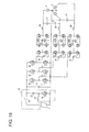
- Fig. 18 illustrates a configuration example of a photovoltaic power system provided with a non-insulating type power conditioner.
- a power conditioner 36 is operated while interconnected to a commercial power source 2.
- the power conditioner 36 includes a smoothing capacitor 33 that smoothes a power-generation output from a photovoltaic panel 1, a PWM-control inverter 34, a filter 35 that includes a reactor and a capacitor, and a control circuit (not illustrated).
- the smoothing capacitor 33 smoothes the power-generation output from the photovoltaic panel 1.
- An inverter34 includes four switch elements 37 to 40 each of which includes a MOSFET connected in reversely parallel to a diode.
- the power-generation output from the photovoltaic panel 1, smoothed by the smoothing capacitor 33 is converted into the AC power synchronized with a commercial power system to output the AC power by switching control in which the switch elements 37 to 40 of the inverter 34 are turned on and off at a frequency as high as about 18 KHz.
- the power conditioner 36 supplies the AC power to a load (not illustrated) through the filter 35 or reversely flows the AC power onto the system side.
- the power converter provided with the conventional power conditioner 36 has low power conversion efficiency because a large switching loss is generated during power conversion of the power conditioner 36.
- the present invention has been devised to solve the problems described above, and an object thereof is to provide a power converter that enhances the conversion efficiency from the DC power into the AC power and a power conditioner provided therewith.
- a power converter includes: first means for chopping a DC voltage at a first frequency to produce a first square-wave voltage string including a plurality of square-wave voltages, a voltage level of the square-wave voltage changing onto a positive side with respect to a first reference potential, the first means including a first switch circuit in which first and second switch elements are connected in series, the first switch circuit being connected in parallel to a first capacitor connected between positive and negative electrodes of a DC power source; second means for chopping an output of the first means at a second frequency higher than the first frequency to produce a second square-wave voltage string including a plurality of square-wave voltages, a voltage level of the square-wave voltage being lower than that of the first square-wave voltage string on the positive side and changing onto a negative side with respect to a second reference potential, a potential at the first square-wave voltage string being set to the second reference potential, the second means producing a third square-wave voltage string by adding the first square-wave voltage
- the first means produces the first square-wave voltage string that changes onto the positive side of the first frequency.
- the second means produces the second square-wave voltage string that changes onto the negative side of the second frequency that is higher than the first frequency, and produces the third square-wave voltage string by adding the first square-wave voltage string and the second square-wave voltage string.
- the third square-wave voltage string alternately changes in the sine-wave manner on the positive and negative sides.
- the third performs the charge and discharge at the third frequency fixed by timing according to the positive or negative of the difference between the third square-wave voltage string and the sine-wave voltage.
- the first to third frequencies that are of the chopping frequencies of the first to third means can be set much lower than the switching frequency of the conventional PWM-control inverter that produces many square-wave voltage strings in a positive or negative half period of the sine wave.
- the number of switching times can be decreased, and an element in which a conduction loss is reduced even if the switching loss is somewhat increased as the switch element can be selected.
- the fourth means performs the PWM control to the voltage of the difference between the third square-wave voltage string and the sine-wave voltage, so that the switching can be performed at a voltage lower than that of the conventional PWM-control inverter. From this point, the switching loss can be reduced in the power converter of the first aspect.
- the power conversion efficiency can be improved compared with the conventional inverter.
- Each of the measuring circuits measures the voltage between both ends of each of the first to third capacitors of the first to third means
- the control means performs ON/OFF control to each of the first to eighth switch elements based on the measured value of each measuring circuit
- the gain calibration means calibrates the gain of each measuring circuit that measures the voltage between both ends of each of the first to third capacitors. Therefore, there is no error such that the measured value varies with respect to the identical voltage due to a variation of components constituting the measuring circuits, which allows a spike noise caused by the error to be prevented from being generated in the output voltage at a moment when the control means switches the turn-on and turn-off of the first to eighth switch element.
- control means controls the first to eighth switch elements while short-circuiting an output of the fourth means such that an identical voltage is applied to both ends of two capacitors in the first capacitor, the second capacitor, and the third capacitor, and the gain calibration means calibrates the gain based on the measured values of the measuring circuits corresponding to the two capacitors to which the identical voltage is applied.
- control means performs the control such that the identical voltage is applied to the two capacitors
- the gain calibration means can calibrate the gain of the measuring circuits corresponding to the two capacitors, and the gain can automatically be calibrated.
- control means sets one of the first capacitor, the second capacitor, and the third capacitor to a reference and performs control such that an identical voltage is applied to both ends of each two capacitors including the reference capacitor, and the gain calibration means calibrates the gains of the two measuring circuits except the reference capacitor based on the measured value of the measuring circuit corresponding to the reference capacitor to which the identical voltage is applied.
- the identical voltage is applied to both ends of each the first and second capacitors
- the gain of the measuring circuit corresponding to the second capacitor can be calibrated based on the measured value of the measuring circuit corresponding to the first capacitor
- the identical voltage is applied to both ends of each the first and third capacitors
- the gain of the measuring circuit corresponding to the third capacitor can be calibrated based on the measured value of the measuring circuit corresponding to the first capacitor.
- a power conditioner that converts a DC power from a DC power source into an AC power interconnected to a system of a commercial power source, the power conditioner includes: first means for chopping a DC voltage at a first frequency that is a system frequency to produce a first square-wave voltage string including a plurality of square-wave voltages, a voltage level of the square-wave voltage changing onto a positive side with respect to a first reference potential, the first means including a first switch circuit in which first and second switch elements are connected in series, the first switch circuit being connected in parallel to a first capacitor connected between positive and negative electrodes of a DC power source; second means for chopping an output of the first means at a second frequency higher than the first frequency by a predetermined number of times to produce a second square-wave voltage string including a plurality of square-wave voltages, a voltage level of the square-wave voltage being lower than that of the first square-wave voltage string on the positive side and changing onto a negative side
- the first to third means produces the third square-wave voltage string that alternately changes in the sine-wave manner on the positive and negative sides, and the charge and discharge are performed according to the positive or negative of the difference between the third square-wave voltage string and the sine-wave voltage.
- the chopping frequencies of the first to third means that is, the switching frequencies of the switch elements can be set much lower than the switching frequency of the conventional PWM-control inverter that produces many square-wave voltage strings in the positive or negative half period of the sine wave.
- the switching loss can be decreased, and the element in which the conduction loss is reduced as the switch element can be selected.
- the fourth means performs the PWM control to the voltage of the difference between the square-wave voltage string and the sine-wave voltage. Each of the square-wave voltage string and the sine-wave voltage alternately changes on the positive and negative sides. Therefore, the switching is performed at a voltage lower than that of the conventional PWM-control inverter, so that the switching loss can be reduced.
- the power conversion efficiency can be improved compared with the conventional power conditioner.
- each of the measuring circuits measures the voltage between both ends of each of the first to and third capacitors
- the control means performs ON/OFF control to each of the first to eighth switch elements based on the measured value of each measuring circuit
- the gain calibration means calibrates the gain of each measuring circuit that measures the voltage between both ends of each of the first to and third capacitors. Therefore, there is no error such that the measured value varies with respect to the identical voltage due to a variation of components constituting the measuring circuits, which allows a spike noise caused by the error to be prevented from being generated in the output voltage at a moment when the control means switches the turn-on and turn-off of the first to eighth switch element.
- the DC voltage is chopped to produce the square-wave voltage string that alternately changes on the positive and negative sides in the sine-wave manner. Therefore, the chopping frequency for producing the square-wave voltage string, that is, the switching frequency of the switch element can be set much lower than the switching frequency of the conventional PWM-control inverter that produces many square-wave voltage strings in the positive or negative half period of the sine wave.
- the switching losses can largely be decreased, and the element in which the conduction loss is reduced as the switch element can be selected.
- the PWM control is performed to the voltage of the difference between the square-wave voltage string and the sine-wave voltage.
- Each of the square-wave voltage string and the sine-wave voltage alternately changes on the positive and negative sides. Therefore, the switching can be performed at a voltage lower than that of the conventional PWM-control inverter.
- the switching loss can be reduced from this point.
- the power conversion efficiency can dramatically be enhanced compared with the conventional example.
- the gain of each measuring circuit that measures the voltage between both ends of each of the first to and third capacitors is calibrated, the error caused by the variation of components constituting the measuring circuits is not generated in the measured value, which allows the spike noise caused by the error to be prevented from being generated in the output voltage at the moment when the control means switches the turn-on and turn-off of the first to eighth switch element.
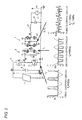
- Fig. 1 is a configuration diagram of a photovoltaic power system according to a first embodiment of the invention, and Fig. 1 illustrates a configuration of the single-phase two-wire system.
- the photovoltaic power system of the first embodiment includes a photovoltaic panel 1 and a power conditioner 3.
- the power conditioner 3 converts the DC power from the photovoltaic panel 1 into the AC power, and the power conditioner 3 is operated while interconnected to a commercial power source 2.
- the photovoltaic panel 1 is configured such that a required generation power is obtained by connecting a plurality of photovoltaic modules in series and in parallel.
- the photovoltaic panel 1 of the first embodiment includes an amorphous silicon thin-film photovoltaic cell.
- the power conditioner of the first embodiment is a non-insulating type (transformer-less) power conditioner that does not includes the insulating transformer.
- the power conditioner 3 includes a first capacitor 4 that is of a smoothing capacitor, first to third chopper circuits 5 to 7, a noise filter 8, and a control circuit 9 that controls each unit.
- the control circuit 9 outputs gate signals to control the first to third chopper circuits 5 to 7.
- the control circuit 9 includes a control unit 9a that calibrates the gain of the measuring circuit and a measuring unit 9b that measures the voltage and output current of each unit.
- the first to third chopper circuits 5 to 7 and the control circuit 9 constitute a chopper converter that is connected in a cascade manner to the photovoltaic panel 1.
- a negative electrode side of the photovoltaic panel 1 is grounded.
- a point (a) illustrated in Fig. 1 is the ground, and the ground has a voltage of zero.
- a point (b) indicates a positive electrode side of the photovoltaic panel 1.
- the first capacitor 4 is connected in parallel between the positive and negative electrodes of the photovoltaic panel 1.
- the first chopper circuit 5 is connected in parallel to the first capacitor 4.
- the first chopper circuit 5 includes first and second switch elements 10 and 11 that are connected in series, Diodes are connected in reversely parallel to the first and second switch elements 10 and 11, respectively.
- the first chopper circuit 5 constitutes a first switch circuit by the first and second switch elements 10 and 11.
- the first and second switch elements 10 and 11 are alternately ON/OFF-controlled at a system frequency, for example, a first frequency f 1 of 50 Hz by a gate signal from the control circuit 9.
- the first and second switch elements 10 and 11 include N-channel MOSFETs similarly to switch elements 12 to 17 of the second and third chopper circuits 6 and 7.
- the switch element may be other switch elements such as an IGBT and a transistor in addition to the MOSFET.
- the second chopper circuit 6 includes a second capacitor 18 and a second switch circuit.
- the third and fourth switch elements 12 and 13 that are connected in series, and each of the switch elements 12 and 13 includes a diode that is connected in reversely parallel.
- the second capacitor 18 and the second switch circuit are connected in parallel.
- the third and fourth switch elements 12 and 13 are alternately ON/OFF-controlled at a second frequency f 2 by a gate signal from the control circuit 9.
- the second frequency f 2 is set to 100 Hz that is double the first frequency f 1 .
- one end side of the parallel connection between the second capacitor 18 and the second switch circuit is connected to the series-connected portion of the first and second switch elements 10 and 11 of the first chopper circuit 5.
- the connection point is illustrated by a point (c) in Fig. 1 .
- the points (c) and (d) correspond to both the capacitor electrode sides of the second capacitor 18.
- the third chopper circuit 7 includes a third switch circuit, a third capacitor 19, and a fourth switch circuit.
- the fifth and sixth switch elements 14 and 15 are connected in series, and each of the switch elements 14 and 15 includes a diode that is connected in reversely parallel.
- the fourth chopper circuit the seventh and eighth switch elements 16 and 17 are connected in series, and each of the switch elements 16 and 17 includes a diode that is connected in reversely parallel.
- the third switch circuit, the third capacitor 19, and the fourth switch circuit are connected in parallel.
- One end side and the other end side of the parallel connection among the circuits are illustrated by points (f) and (g) in Fig. 1 .
- the points (f) and (g) correspond to both the capacitor electrode sides of the third capacitor 19.
- the fifth and sixth switch elements 14 and 15 are alternately ON/OFF-controlled at a third frequency f 3 by a gate signal from the control circuit 9.
- the third frequency f 3 is set to 150 Hz that is triple the first frequency f 1 .
- the seventh and eighth switch elements 16 and 17 are alternately PWM-controlled at a high frequency f4 of, for example, 18 KHz by a gate signal from the control circuit 9.
- the series-connected portion of the fifth and sixth switch elements 14 and 15 of the third chopper circuit 7 is connected to the series-connected portion of the third and fourth switch elements 12 and 13 of the second chopper circuit 6.
- the connection point is illustrated by a point (e) in Fig. 1 .
- the noise filter 8 including a reactor 20 and a fourth capacitor 21 is connected to the series-connected portion of the seventh and eighth switch elements 16 and 17 of the third chopper circuit 7.
- the connection point is illustrated by a point (h) in Fig. 1 .
- a load (not illustrated) and the commercial power source 2 are connected to the noise filter 8.
- the control circuit 9 measures a system voltage Vs and a system current Is through a differential amplifying circuit (not illustrated) of the measuring unit 9b to compute a command value V* of a sine-wave target voltage synchronized with a system frequency of the commercial power source 2 as is conventionally done, and the control circuit 9 measures voltages Vd1, Vd2, and Vd3 at both ends of the first to third capacitors 4, 18, and 19 to produce the gate signals in order to control the chopper circuits 5 to 7.
- the voltage Vd1 is a DC output voltage of the photovoltaic panel 1, which emerges at the point (b) based on the voltage at the point (a) that is the ground.
- the voltage Vd2 is a charge voltage at the point (c) of one of the capacitor electrodes of the second capacitor 18 in the second chopper circuit 6 based on the point (d) of the other capacitor electrode in the second capacitor 18.
- the voltage Vd3 is a charge voltage at the point (g) of one of the capacitor electrodes of the third capacitor 19 in the third chopper circuit 7 based on the point (f) of the other capacitor electrode in the third capacitor 19.
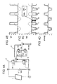
- Fig. 2 is a schematic diagram for explaining an operation of each of the chopper circuits 5 to 7 of the embodiment
- Fig. 2A illustrates a configuration of a main part of Fig. 1
- Fig. 2B to Fig. 2D illustrates voltages V1, V2, and V3 of Fig. 2A
- Fig. 2B and Fig. 2C the waveform of the command value V* of the sine-wave target voltage synchronized with the system is illustrated by a thin solid line.
- the voltage V1 is a voltage at the point (c) that is of the series-connected portion of the first and second switch elements 10 and 11 of the first chopper circuit 5 when a potential at the point (a) that is of the ground is set to a first reference potential.
- the voltage V2 is a voltage at the point (e) that is of the series-connected portion of the third and fourth switch elements 12 and 13 of the second chopper circuit 6 when a potential at the point (c) is set to a second reference potential.
- the voltage V3 is a voltage at the point (h) that is of the series-connected portion of the seventh and eighth switch elements 16 and 17 based on the point (e) that is of the series-connected portion of the fifth and sixth switch elements 14 and 15 in the third chopper circuit 7.
- the first and second switch elements 10 and 11 are alternately ON/OFF-controlled at the first frequency f 1 of 50 Hz when the first frequency f 1 is identical to the system frequency of 50 Hz of the commercial power source 2.
- the voltage V1 at the point (c) that is of the series-connected portion of the first and second switch elements 10 and 11 becomes a first square-wave voltage string including a plurality of square-wave voltages that rise on a positive side as illustrated in Fig. 2B .
- a square-wave voltage level of the voltage V1 becomes the DC output voltage Vd1 of the photovoltaic panel 1.
- the third and fourth switch elements 12 and 13 are alternately ON/OFF-controlled at the second frequency f 2 of 100 Hz that is double the first frequency f 1 .
- the voltage V2 at the point (e) that is of the series-connected portion of the third and fourth switch elements 12 and 13 becomes a second square-wave voltage string including a plurality of square-wave voltages that fall on a negative side based on the point (c) that is of the series-connected portion of the first and second switch elements 10 and 11.
- a square-wave voltage level of the voltage V2 is controlled so as to become a half of the DC output voltage Vd1.
- the voltage V2 at the point (e) that is of the series-connected portion of the third and fourth switch elements 12 and 13 of the second chopper circuit 6 becomes a voltage V1 + V2 that is the sum of the voltage V1 between the points (a) and (c) and the voltage V2 between the voltage V2 between the points (c) and (e) based on the point (a) that is of the ground, that is, the first reference potential.
- the voltage V1 + V2 has a stepwise waveform corresponding to the sine wave that alternately changes positively and negatively.
- the stepwise voltage V1 + V2 alternately changes positively and negatively in synchronization with the command value V* of the sine-wave target voltage illustrated by the thin solid line of Fig. 4D .
- the fifth and sixth switch elements 14 and 15 are alternately ON/OFF-controlled at the third frequency f 3 of 150 Hz that is triple the first frequency f 1 so as to compensate a difference voltage between the voltage V1 + V2 having the stepwise waveform and the command value V* of the sine-wave target voltage, and the seventh and eighth switch elements 16 and 17 are PWM-controlled at the frequency f4 of 18 KHz.
- the voltage V3 at the point (h) that is of the series-connected portion of the seventh and eighth switch elements 16 and 17 of the third chopper circuit 7 illustrated in Fig. 2A corresponds to the difference voltage between the voltage V1 + V2 ( Fig. 4D ) having the stepwise waveform and the command value V* of the sine-wave target voltage when being illustrated by an average value of PWM based on the point (e) that is of the series-connected portion of the fifth and sixth switch elements 14 and 15.
- the voltage V3 at the point (h) that is of the series-connected portion of the seventh and eighth switch elements 16 and 17 of the third chopper circuit 6 becomes a sine-wave voltage corresponding to the command value V* of the sine-wave target voltage synchronized with the commercial power source 2 based on the first reference potential at the point (a) that is of the ground.
- Fig. 3 is a view for explaining the operation principle of the first chopper circuit 5
- Fig. 3A illustrates the photovoltaic panel 1, the first capacitor 4, and the first chopper circuit 5
- Fig. 3B illustrates the voltage V1 between the points (a) and (c).
- the command value V* of the sine-wave target voltage is illustrated by the thin solid line.
- the DC output voltage Vd1 of the photovoltaic panel 1 emerges at the point (b) on the positive electrode side of the photovoltaic panel 1.
- the DC output voltage Vd1 is smoothed by the first capacitor 4 when the potential at the point (a) that is of the ground is set to the first reference potential.
- the DC output voltage Vd1 is chopped by the first and second switch elements 10 and 11 that are alternately ON/OFF-controlled at the first frequency f 1 of 50 Hz.
- the voltage V1 at the point (c) that is of the series-connected portion of the first and second switch elements 10 and 11 becomes the first square-wave voltage string including the plurality of square-wave voltages that rise on the positive side when the ground potential is set to the first reference potential as illustrated in Fig. 3B .
- the voltage V1 is the voltage at the point (c) that is of the series-connected portion of the first and second switch elements 10 and 11 based on the point (a), and the square-wave voltage level becomes the DC output voltage Vd1 of the photovoltaic panel 1, for example, 800 V.
- the effective power can be output because the square-wave voltage string whose phase is matched with that of the system voltage is produced.
- Fig. 4 is a view for explaining the operation principle of the second chopper circuit 6, Fig. 4A illustrates the first chopper circuit 5 and the second chopper circuit 6, Fig. 4B illustrates the voltage V1, Fig. 4C illustrates the voltage V2, and Fig. 4D illustrates the voltage V1 + V2.
- the command value V* of the sine-wave target voltage is also illustrated by the thin solid line.
- the voltage V1 at the point (c) illustrated in Fig. 4B is chopped by the third and fourth switch elements 12 and 13 that are alternately ON/OFF-controlled at the second frequency f 2 of 100 Hz.
- the potential at the point (e) that is of the series-connected portion of the third and fourth switch elements 12 and 13 becomes the same potential as the point (c) that is of the series-connected portion of the first and second switch elements 10 and 11 of the first chopper circuit 5.
- the potential at the point (e) that is of the series-connected portion of the third and fourth switch elements 12 and 13 becomes more negative than the potential at the point (c).
- the voltage V2 at the point (e) that is of the series-connected portion of the third and fourth switch elements 12 and 13 becomes the second square-wave voltage string including the plurality of square-wave voltages that fall on the negative side when the potential at the point (c) that is of the series-connected portion of the first and second switch elements 10 and 11 is set to the second reference potential as illustrated in Fig. 4C .
- the charge during a charge period T1 and the discharge during a discharge period T2 are alternately repeated to produce the square-wave voltage that falls on the negative side based on the second reference potential at the point (c).
- the voltage V2 is a voltage at the point (e) that is of the series-connected portion of the third and fourth switch elements 12 and 13 based on the point (c) that is of the series-connected portion of the first and second switch elements 10 and 11. Accordingly, in the second chopper circuit6, the voltage V1 + V2 that is the sum of the voltage V1 between the points (a) and (c) illustrated in Fig. 4B and the voltage V2 between the points (c) and (e) illustrated in Fig. 4C emerges at the point (e) when the point (a) that is of the ground is set to the first reference potential.
- the voltage V1 + V2 has the stepwise waveform that alternately changes positively and negatively according to the change of the command value V* of the sine-wave target voltage illustrated in Fig. 4D .
- the system current Is of Fig. 9C is passed through the second capacitor 18, thereby performing the charge and the discharge.
- the system current Is of Fig. 9C is positive, the second capacitor 18 is charged by the sine-wave current during the period T1 of Fig. 4C . Therefore, the voltage V2 is gradually decreased during the period T1 in the actual operation.
- the system current Is of Fig. 9C is negative, the second capacitor 18 is discharged by the sine-wave current during the period T2 of Fig. 4C . Therefore, the voltage V2 is gradually increased during the period T2 in the actual operation.
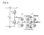
- Fig. 5 is a view for explaining the operation principle of the third chopper circuit 7
- Fig. 6A illustrates the voltage V1 + V2 having the stepwise waveform
- Fig. 6B illustrates the voltage V3 at the point (h) that is of the series-connected portion of the seventh and eighth switch elements 16 and 17 as the average value of PWM based on the point (e) that is of the series-connected portion of the fifth and sixth switch elements 14 and 15.
- the command value V* of the sine-wave target voltage is also illustrated by the thin solid line.
- the fifth and sixth switch elements 14 and 15 are ON/OFF-controlled in timing corresponding to the positive and negative of the difference voltage between the voltage V1 + V2 having the stepwise waveform at the point (e) illustrated in Fig. 6A and the command value V* of the sine-wave target voltage.
- the third capacitor 19 is charged and discharged by the voltage V1 + V2 at the time the fifth and sixth switch elements 14 and 15 are ON/OFF-controlled.
- a period of a magnitude relation of the difference voltage is the third frequency f 3 of 150 Hz, and therefore the fifth and sixth switch elements 14 and 15are alternately ON/OFF-controlled at the third frequency f 3 .
- the seventh and eighth switch elements 16 and 17 are PW M-controlled at the fourth frequency f4 that is hundreds times the first frequency f 1 with a duty that corrects the difference voltage between the voltage V1 + V2 and the command value V* of the sine-wave target voltage. Therefore, as illustrated in Fig. 6B , the voltage V3 corresponding to the difference voltage between the voltage V1 + V2 having the stepwise waveform and the command value V* of the sine-wave target voltage emerges at the point (h) that is of the series-connected portion of the seventh and eighth switch elements 16 and 17.
- the voltage V3 indicates the average value of the PWM, and the voltage V3 is a voltage at the point (h) that is of the series-connected portion of the seventh and eighth switch elements 16 and 17 based on the point (e) that is of the series-connected portion of the fifth and sixth switch elements 14 and 15.
- the command value V* of the sine-wave target voltage whose phase is identical to that of the change in power system frequency illustrated by the thin solid line of Fig. 6A at the point (h) that is of the series-connected portion of the seventh and eighth switch elements 16 and 17 based on the first reference potential at the point (a) that is of the ground.
- the command value V* of the sine-wave target voltage is the sum of the voltage V1 + V2 between the points (a) and (e) illustrated in Fig. 6A and the voltage V3 between the points (e) and (h) illustrated in Fig. 6B .
- the difference with the sine-wave voltage is eliminated while the chopping is performed at the frequency that is triple the system frequency, so that at least three-order high-harmonic can be suppressed.
- the control circuit 9 controls pulse widths of the plurality of square-wave voltages that rise on the positive side of Fig. 3B using the gate signal output to the first and second switch elements 10 and 11 of the first chopper circuit 5.
- a fundamental-wave component of the output voltage of the first chopper circuit 5 is controlled so as to be matched with a fundamental-wave voltage of a system power source, and a pulse width ⁇ of the square-wave voltage is controlled so as to become a value computed by the following equation.
- V is an effective value of a voltage Vs of the system power source.
- the fundamental-wave voltage can be increased and decreased when the pulse width is adjusted by ⁇ 1, and ⁇ 1 is computed by multiplying a factor by an error between the measured voltage Vd3 and the target voltage Vd3*.
- control circuit 9 uses the gate signal output to the third and fourth switch elements 12 and 13 of the second chopper circuit 6, the control circuit 9 performs the control such that voltage Vd2 illustrated in Fig. 4C becomes a half of the voltage Vd1 of the first chopper circuit 5.
- the second capacitor 18 repeats the charge and discharge to produce the plurality of square-wave voltage strings that rise on the negative side illustrated in Fig. 4C .
- the charge period T1 that is, the pulse width of the square wave corresponding to the charge is identical to the pulse width of the square wave output from the first chopper circuit 5, and the discharge period T2, that is, the pulse width of the square wave corresponding to the discharge is a pulse width in which the pulse width of the square wave corresponding to the charge is finely adjusted only by ⁇ 2 ,
- ⁇ 2 is computed by multiplying a factor by an error between the measured voltage Vd2 and the target voltage Vd2*.
- the target voltage Vd2* is set to the voltage that is a half of the measured voltage Vd1.
- the control circuit 9 controls the pulse width of the square-wave voltage according to a fluctuation in power-generation output of the photovoltaic panel 1.
- Fig. 7 and Fig. 8 illustrate simulation waveforms of the positive-side and negative-side square-wave voltages V1 and V2 when the input voltage Vd1 from the photovoltaic panel 1 fluctuates.
- Fig. 7 illustrates the input voltage Vd1 of 800 V
- Fig. 8 illustrates the input voltage Vd 1 of 520 V.
- Fig. 7A and Fig. 8A illustrate the command value V* of the sine-wave target voltage.
- Fig. 7B and Fig. 8B illustrate the positive-side voltage V1 by the first chopper circuit 5.
- Fig. 7C and Fig. 8C illustrate the negative-side voltage V2 by the second chopper circuit 6.
- both the pulse widths of the positive-side square wave illustrated in Fig. 8B and the negative-side square wave illustrated in Fig. 8C are controlled so as to be widened compared with those of Fig. 7 .
- the control circuit 9 alternately performs the ON/OFF control to the fifth and sixth switch elements 14 and 15 of the third chopper circuit 7 in timing according to the positive or negative of the difference between the stepwise voltage V1 + V2 illustrated in Fig. 6A and the command value V* of the sine-wave target voltage, and the control circuit 9 performs the PWM control to the seventh and eighth switch elements 16 and 17 at a high frequency with a duty that corrects the difference voltage, thereby producing the sine-wave voltage of the command value V* of the sine-wave target voltage.
- Fig. 9 illustrates a simulation waveform of each unit of Fig. 1 , and the simulation waveform is obtained based on the ground.
- Fig. 9A illustrates the system voltage Vs
- Fig. 9B illustrates the output voltage V of the third chopper circuit 7
- Fig. 9C illustrates the system current Is
- Fig. 9D illustrates the voltage V1 and V2 (broken line)
- Fig. 9E illustrates the voltage V3
- Fig. 9F illustrates the voltages Vd2 and Vd3 (broken line).
- the first and second switch elements 10 and 11 of the first chopper circuit 5 switch the voltage of 800 V at the first frequency f 1 of 50 Hz
- the third and fourth switch elements 12 and 13 of the second chopper circuit 6 switch the voltage of 400 V at the second frequency f 2 of 100 Hz
- the fifth and sixth switch elements 14 and 15 of the third chopper circuit7 switch the voltage of 260 V at the third frequency f 3 of 150 Hz. That is, the switch elements 10 to 15 perform the switching at the frequencies that are much lower than the PWM frequency of the conventional PWM-control power conditioner.
- the seventh and eighth switch elements 16 and 17 of the third chopper circuit 7 performs the PWM control to the voltage of about 260 V that is of the difference voltage between the stepwise voltage V1 + V2 and the command value V* of the sine-wave target voltage at a frequency as high as 18 KHz. That is, the seventh and eighth switch elements 16 and 17 switch the voltage that is lower than that of the PWM-control inverter of the conventional power conditioner.
- the first to sixth switch elements 10 to 15 of the first to third chopper circuits 5 to 7 perform the switching at the frequencies that is much lower than those of the conventional PWM control, so that the switching loss can be reduced and the low-conduction-loss switch element or the inexpensive switch element can be selected.
- the seventh and eighth switch elements 16 and 17 of the third chopper circuit 7 switch the voltage that is lower than that of the conventional PWM control, so that the switching loss can be reduced.
- the power conversion efficiency of the power conditioner 3 can be improved compared with the conventional power conditioner.
- the square-wave voltage producing means includes the first chopper circuit 5, the second chopper circuit 6, the fifth and sixth switch elements 14 and 15 and the third capacitor 19 of the third chopper circuit 7, and the control circuit 9 that controls each unit.
- the sine-wave voltage producing means includes the seventh and eighth switch elements 16 and 17 of the third chopper circuit 7 and the control circuit 9 that controls the switch elements 16 and 17.
- the photovoltaic panel 1 includes the amorphous silicon thin-film photovoltaic cell.
- the negative electrode side of the photovoltaic cell which is of the input side of the power conditioner 36, cannot be set to the ground potential.
- the negative electrode side of the photovoltaic cell can be set to the ground potential.
- the photovoltaic power system is applied to the single-phase two-wire system.
- the photovoltaic power system of the invention may be applied to a single-phase three-wire system illustrated in Fig. 10 , a three-phase three-wire system illustrated in Fig. 11 , and a three-phase four-wire system illustrated in Fig. 12 .
- Fig. 13 illustrates comparison of characteristics of a three-phase four-wire system of an embodiment of the invention illustrated in Fig. 15 and a conventional system illustrated in Fig. 14 .
- a horizontal axis indicates the output power (W) and a vertical axis indicates the efficiency (%).
- the solid line expresses the characteristic of the embodiment, a bold solid line expresses the characteristic in which an SJ (Super Junction) MOSFET is used as the switch element, a thin solid line expresses the characteristic in which an IGBT is used as the switch element, and a broken line expresses the characteristic of the conventional system.
- SJ Super Junction
- Fig. 13 illustrates the characteristics for the inter-system-line voltage of 400 V and the input voltage of 570 V.
- the conventional system is the non-insulating type power conditioner including a boost circuit 32, a smoothing capacitor 41, and a PWM-control inverter 42.
- the boost circuit 32 includes a reactor 28, a diode 29, an IGBT 30, and a switch 31.
- the efficiency is improved compared with the conventional system.
- the following method is adopted such that the spike noise is not generated in the output voltage.
- the command value V* of the sine-wave target voltage is computed by referring to the measured voltages Vd1, Vd2, and Vd3.
- the voltages Vd1, Vd2, and Vd3 are measured by the corresponding measuring circuits in the measuring unit 9b of the control circuit 9. Occasionally the measured value varies even at the identical voltage due to the variation of components constituting the measuring circuits, and particularly, the difference of the measured value is increased in a high-temperature place or a low-temperature place.
- the gains of the measuring circuits are automatically calibrated such that the measured values of the measuring circuits are matched with one another with respect to the identical measuring voltage.
- the gains of the measuring circuits corresponding to the voltages Vd2 and Vd3 are calibrated based on the measuring circuit corresponding to the voltage Vd1.
- Fig. 16 is a configuration diagram illustrating the case in which the measuring circuit corresponding to the voltage Vd2 is calibrated based on the measuring circuit corresponding to the voltage Vd1.
- the portion corresponding to that of Fig. 1 is designated by the identical reference numeral.
- an output short-circuit relay 50 is closed while an interconnecting relay (not illustrated) is opened to separate the photovoltaic power system from the system of the commerial power source, and the ON/OFF control is performed to the switch elements 10 to 17 such that the voltage Vd1 at both ends of the first capacitor 4 and the voltage Vd2 at both ends of the second capacitor 18 become identical.
- the first switch element 10, the fourth switch element 13, the sixth switch element 15, and the eighth switch element 17 are turned on while the second switch element 11, the third switch element 12, the fifth switch element 14, and the seventh switch element 16 are turned off, and the switching is controlled such that the voltage Vd1 at both ends of the first capacitor 4 and the voltage Vd2 at both ends of the second capacitor 18 become identical.
- a correction factor is computed by the following equation in order to perform the correction such that the measured value of the measuring circuit corresponding to the voltage Vd2 is matched with the measured value of the measuring circuit corresponding to the voltage Vd1.
- correction factor (measured value of voltage Vd1) / (measured value of voltage Vd2)
- the post-correction measured value in which the measured value of the voltage Vd2 is corrected can be obtained by multiplying the correction factor by the measured value (pre-correction measured value) of the voltage Vd2 measured by the measuring circuit.
- the post-correction measured value of the voltage Vd2 is computed by the following equation.
- the measured value of the measuring circuit corresponding to the voltage Vd1 and the measured value of the measuring circuit corresponding to the voltage Vd2 can be matched with each other with respect to the identical voltage.
- Fig. 17 is a configuration diagram illustrating the case in which the measuring circuit corresponding to the voltage Vd3 is calibrated based on the measuring circuit corresponding to the voltage Vd1.
- the portion corresponding to that of Fig. 1 is designated by the identical reference numeral.
- the output short-circuit relay 50 is closed while the interconnecting relay is opened to separate the photovoltaic power system from the system of the commercial power source, and the ON/OFF control is performed to the switch elements 10 to 17 such that the voltage Vd1 at both ends of the first capacitor 4 and the voltage Vd3 at both ends of the third capacitor 19 become identical.
- the first switch element 10, the third switch element 12, the fifth switch element 14, and the eighth switch element 17 are turned on while the second switch element 11, the fourth switch element 13, the sixth switch element 15, and the seventh switch element 16 are turned off, and the switching is controlled such that the voltage Vd1 at both ends of the first capacitor 4 and the voltage Vd3 at both ends of the third capacitor 19 become identical.
- a correction factor is computed by the following equation in order to perform the correction such that the measured value of the measuring circuit corresponding to the voltage Vd3 is matched with the measured value of the measuring circuit corresponding to the voltage Vd1.
- correction factor measured value of voltage Vd1 / measured value of voltage Vd3
- the post-correction measured value in which the measured value of the voltage Vd3 is corrected can be obtained by multiplying the correction factor by the measured value (pre-correction measured value) of the voltage Vd3 measured by the measuring circuit.
- the post-correction measured value of the voltage Vd3 is computed by the following equation.
- the measured value of the measuring circuit corresponding to the voltage Vd1 and the measured value of the measuring circuit corresponding to the voltage Vd3 can be matched with each other with respect to the identical voltage.
- the measured values of the measuring circuits corresponding to the voltages Vd1, Vd2, and Vd3 can be matched with one another with respect to the identical voltage, so that the AC-voltage spike noise caused by the error of the measured value can be suppressed.
- the invention is useful to the power converter.
Landscapes
- Engineering & Computer Science (AREA)
- Power Engineering (AREA)
- Inverter Devices (AREA)
- Supply And Distribution Of Alternating Current (AREA)
Applications Claiming Priority (1)
| Application Number | Priority Date | Filing Date | Title |
|---|---|---|---|
| JP2010052761A JP5071498B2 (ja) | 2010-03-10 | 2010-03-10 | 電力変換装置およびパワーコンディショナ |
Publications (3)
| Publication Number | Publication Date |
|---|---|
| EP2365626A2 true EP2365626A2 (de) | 2011-09-14 |
| EP2365626A3 EP2365626A3 (de) | 2014-05-28 |
| EP2365626B1 EP2365626B1 (de) | 2017-03-15 |
Family
ID=44262898
Family Applications (1)
| Application Number | Title | Priority Date | Filing Date |
|---|---|---|---|
| EP11151243.0A Not-in-force EP2365626B1 (de) | 2010-03-10 | 2011-01-18 | Wechselrichter mit Leistungsfaktorkorrektur |
Country Status (5)
| Country | Link |
|---|---|
| US (1) | US8462526B2 (de) |
| EP (1) | EP2365626B1 (de) |
| JP (1) | JP5071498B2 (de) |
| KR (1) | KR101186364B1 (de) |
| CN (1) | CN102195500B (de) |
Cited By (2)
| Publication number | Priority date | Publication date | Assignee | Title |
|---|---|---|---|---|
| EP2778824A3 (de) * | 2013-03-15 | 2014-09-24 | Omron Corporation | Inverter und Programm |
| EP2618474A4 (de) * | 2010-09-13 | 2015-12-02 | Omron Tateisi Electronics Co | Spannungsversorgungsgerät |
Families Citing this family (10)
| Publication number | Priority date | Publication date | Assignee | Title |
|---|---|---|---|---|
| TWI481146B (zh) * | 2011-12-02 | 2015-04-11 | 達方電子股份有限公司 | 太陽能無電池離網型換流器系統及其控制方法 |
| CN102938575B (zh) * | 2012-11-21 | 2014-09-17 | 无锡北方湖光光电有限公司 | 便携式通用野战电源保障系统 |
| US10862404B2 (en) * | 2015-07-14 | 2020-12-08 | Mitsubishi Electric Corporation | Power conversion device including an asymmetrical carrier signal generator |
| US10141851B2 (en) * | 2016-03-25 | 2018-11-27 | General Electric Company | Resonant DC to DC power converter |
| CN109565245B (zh) * | 2016-08-12 | 2021-07-09 | 马里奇控股荷兰有限公司 | 劣化光伏板的恢复 |
| JP2018152996A (ja) * | 2017-03-13 | 2018-09-27 | オムロン株式会社 | 分散型電源 |
| AU2017409798A1 (en) * | 2017-04-10 | 2019-11-07 | Berner Fachhochschule | Efficient electric power conversion |
| US11005388B2 (en) * | 2019-02-28 | 2021-05-11 | sonnen, Inc. | Single-phase multi-level asymmetric inverter with AC-bypass and asymmetric modulation strategy |
| WO2021092537A1 (en) * | 2019-11-08 | 2021-05-14 | Fohtung Edwin | High-voltage power supply system |
| WO2024105841A1 (ja) * | 2022-11-17 | 2024-05-23 | 三菱電機株式会社 | 電力変換装置、および飛行物体 |
Citations (1)
| Publication number | Priority date | Publication date | Assignee | Title |
|---|---|---|---|---|
| JP2002010496A (ja) | 2000-06-16 | 2002-01-11 | Omron Corp | 太陽光発電システムにおけるパワーコンディショナ |
Family Cites Families (20)
| Publication number | Priority date | Publication date | Assignee | Title |
|---|---|---|---|---|
| US4674024A (en) * | 1986-06-05 | 1987-06-16 | Westinghouse Electric Corp. | High voltage modular inverter and control system thereof |
| DE19720787A1 (de) * | 1997-05-17 | 1998-11-19 | Asea Brown Boveri | Verfahren zum Betrieb einer leistungselektronischen Schaltungsanordnung |
| JP3418906B2 (ja) * | 1997-12-24 | 2003-06-23 | オムロン株式会社 | Dc/dcコンバータおよびパワーコンディショナ |
| JP2000116005A (ja) * | 1998-10-02 | 2000-04-21 | Sanken Electric Co Ltd | 交流電源装置 |
| JP2002252986A (ja) * | 2001-02-26 | 2002-09-06 | Canon Inc | インバータ、電源システム及び電源システムにおける漏れ電流低減方法 |
| US6556461B1 (en) * | 2001-11-19 | 2003-04-29 | Power Paragon, Inc. | Step switched PWM sine generator |
| FR2858725B1 (fr) * | 2003-08-06 | 2005-10-07 | St Microelectronics Sa | Dispositif autoreparable pour generer une haute tension, et procede de reparation d'un dispositif pour generer une haute tension. |
| US7596008B2 (en) * | 2005-02-25 | 2009-09-29 | Mitsubishi Electric Corporation | Power conversion apparatus |
| TW200709544A (en) * | 2005-08-29 | 2007-03-01 | Ind Tech Res Inst | Transformer-free power conversion circuit for parallel connection with commercial electricity system |
| JP2007166874A (ja) * | 2005-12-16 | 2007-06-28 | Toyota Motor Corp | 電圧変換装置 |
| JP4755504B2 (ja) * | 2006-02-16 | 2011-08-24 | 三菱電機株式会社 | 電力変換装置 |
| US7692938B2 (en) * | 2006-09-06 | 2010-04-06 | Northern Power Systems, Inc. | Multiphase power converters and multiphase power converting methods |
| US7974106B2 (en) * | 2007-05-07 | 2011-07-05 | Bloom Energy Corporation | Ripple cancellation |
| JP4968465B2 (ja) * | 2007-07-18 | 2012-07-04 | 三菱電機株式会社 | 電力変換装置 |
| US8422257B2 (en) * | 2008-06-09 | 2013-04-16 | Abb Technology Ag | Voltage source converter |
| US20100141230A1 (en) * | 2008-07-17 | 2010-06-10 | Exar Corporation | Self-tuning sensorless digital current-mode controller with accurate current sharing for multiphase dc-dc converters |
| KR100975925B1 (ko) * | 2008-07-25 | 2010-08-13 | 삼성전기주식회사 | 어댑터 전원장치 |
| JP5480296B2 (ja) * | 2009-01-29 | 2014-04-23 | ブルサ エレクトロニック アーゲー | 単相および3相動作用の変換器、dc電源および電池充電器 |
| JP4888817B2 (ja) * | 2009-03-13 | 2012-02-29 | オムロン株式会社 | パワーコンディショナおよび太陽光発電システム |
| JP4911733B2 (ja) * | 2009-03-13 | 2012-04-04 | オムロン株式会社 | 電力変換装置、パワーコンディショナ、および発電システム |
-
2010
- 2010-03-10 JP JP2010052761A patent/JP5071498B2/ja active Active
-
2011
- 2011-01-05 KR KR1020110000824A patent/KR101186364B1/ko active Active
- 2011-01-18 EP EP11151243.0A patent/EP2365626B1/de not_active Not-in-force
- 2011-02-24 US US13/034,056 patent/US8462526B2/en active Active
- 2011-02-25 CN CN201110046134.3A patent/CN102195500B/zh not_active Expired - Fee Related
Patent Citations (1)
| Publication number | Priority date | Publication date | Assignee | Title |
|---|---|---|---|---|
| JP2002010496A (ja) | 2000-06-16 | 2002-01-11 | Omron Corp | 太陽光発電システムにおけるパワーコンディショナ |
Cited By (2)
| Publication number | Priority date | Publication date | Assignee | Title |
|---|---|---|---|---|
| EP2618474A4 (de) * | 2010-09-13 | 2015-12-02 | Omron Tateisi Electronics Co | Spannungsversorgungsgerät |
| EP2778824A3 (de) * | 2013-03-15 | 2014-09-24 | Omron Corporation | Inverter und Programm |
Also Published As
| Publication number | Publication date |
|---|---|
| KR101186364B1 (ko) | 2012-09-26 |
| JP2011188663A (ja) | 2011-09-22 |
| CN102195500A (zh) | 2011-09-21 |
| US20110235384A1 (en) | 2011-09-29 |
| CN102195500B (zh) | 2014-01-22 |
| JP5071498B2 (ja) | 2012-11-14 |
| KR20110102143A (ko) | 2011-09-16 |
| EP2365626B1 (de) | 2017-03-15 |
| US8462526B2 (en) | 2013-06-11 |
| EP2365626A3 (de) | 2014-05-28 |
Similar Documents
| Publication | Publication Date | Title |
|---|---|---|
| EP2365626B1 (de) | Wechselrichter mit Leistungsfaktorkorrektur | |
| EP2234265B1 (de) | Stromumwandlungsvorrichtung, Stromversorgungsgerät und Stromerzeugungssystem | |
| US8184461B2 (en) | Power conditioner and solar photovoltaic power generation system | |
| US20110221281A1 (en) | Method for detecting capacity leakage of capacitor in power conditioner, power conditioner performing the same, and photovoltaic power system provided with the same | |
| US12009690B2 (en) | Power converters and methods of controlling same | |
| US8570781B2 (en) | Power conditioner | |
| JP2024023924A (ja) | 電源システム | |
| JP5410551B2 (ja) | 電力変換装置 | |
| US8902620B2 (en) | Power conditioner | |
| KR101246398B1 (ko) | 제어 회로, 이 제어 회로를 구비하는 파워 컨디셔너, 및 태양광 발전 시스템 |
Legal Events
| Date | Code | Title | Description |
|---|---|---|---|
| PUAI | Public reference made under article 153(3) epc to a published international application that has entered the european phase |
Free format text: ORIGINAL CODE: 0009012 |
|
| AK | Designated contracting states |
Kind code of ref document: A2 Designated state(s): AL AT BE BG CH CY CZ DE DK EE ES FI FR GB GR HR HU IE IS IT LI LT LU LV MC MK MT NL NO PL PT RO RS SE SI SK SM TR |
|
| AX | Request for extension of the european patent |
Extension state: BA ME |
|
| PUAL | Search report despatched |
Free format text: ORIGINAL CODE: 0009013 |
|
| AK | Designated contracting states |
Kind code of ref document: A3 Designated state(s): AL AT BE BG CH CY CZ DE DK EE ES FI FR GB GR HR HU IE IS IT LI LT LU LV MC MK MT NL NO PL PT RO RS SE SI SK SM TR |
|
| AX | Request for extension of the european patent |
Extension state: BA ME |
|
| RIC1 | Information provided on ipc code assigned before grant |
Ipc: H02M 7/49 20070101AFI20140423BHEP |
|
| 17P | Request for examination filed |
Effective date: 20141128 |
|
| RBV | Designated contracting states (corrected) |
Designated state(s): AL AT BE BG CH CY CZ DE DK EE ES FI FR GB GR HR HU IE IS IT LI LT LU LV MC MK MT NL NO PL PT RO RS SE SI SK SM TR |
|
| REG | Reference to a national code |
Ref country code: DE Ref legal event code: R079 Ref document number: 602011035866 Country of ref document: DE Free format text: PREVIOUS MAIN CLASS: H02M0007490000 Ipc: H02M0001420000 |
|
| GRAP | Despatch of communication of intention to grant a patent |
Free format text: ORIGINAL CODE: EPIDOSNIGR1 |
|
| RIC1 | Information provided on ipc code assigned before grant |
Ipc: H02M 7/49 20070101ALI20160829BHEP Ipc: H02M 1/42 20070101AFI20160829BHEP |
|
| INTG | Intention to grant announced |
Effective date: 20160915 |
|
| STAA | Information on the status of an ep patent application or granted ep patent |
Free format text: STATUS: GRANT OF PATENT IS INTENDED |
|
| GRAS | Grant fee paid |
Free format text: ORIGINAL CODE: EPIDOSNIGR3 |
|
| GRAA | (expected) grant |
Free format text: ORIGINAL CODE: 0009210 |
|
| STAA | Information on the status of an ep patent application or granted ep patent |
Free format text: STATUS: THE PATENT HAS BEEN GRANTED |
|
| AK | Designated contracting states |
Kind code of ref document: B1 Designated state(s): AL AT BE BG CH CY CZ DE DK EE ES FI FR GB GR HR HU IE IS IT LI LT LU LV MC MK MT NL NO PL PT RO RS SE SI SK SM TR |
|
| REG | Reference to a national code |
Ref country code: CH Ref legal event code: EP Ref country code: GB Ref legal event code: FG4D |
|
| REG | Reference to a national code |
Ref country code: IE Ref legal event code: FG4D |
|
| REG | Reference to a national code |
Ref country code: AT Ref legal event code: REF Ref document number: 876481 Country of ref document: AT Kind code of ref document: T Effective date: 20170415 |
|
| REG | Reference to a national code |
Ref country code: DE Ref legal event code: R096 Ref document number: 602011035866 Country of ref document: DE |
|
| REG | Reference to a national code |
Ref country code: NL Ref legal event code: MP Effective date: 20170315 |
|
| REG | Reference to a national code |
Ref country code: LT Ref legal event code: MG4D |
|
| PG25 | Lapsed in a contracting state [announced via postgrant information from national office to epo] |
Ref country code: NO Free format text: LAPSE BECAUSE OF FAILURE TO SUBMIT A TRANSLATION OF THE DESCRIPTION OR TO PAY THE FEE WITHIN THE PRESCRIBED TIME-LIMIT Effective date: 20170615 Ref country code: HR Free format text: LAPSE BECAUSE OF FAILURE TO SUBMIT A TRANSLATION OF THE DESCRIPTION OR TO PAY THE FEE WITHIN THE PRESCRIBED TIME-LIMIT Effective date: 20170315 Ref country code: GR Free format text: LAPSE BECAUSE OF FAILURE TO SUBMIT A TRANSLATION OF THE DESCRIPTION OR TO PAY THE FEE WITHIN THE PRESCRIBED TIME-LIMIT Effective date: 20170616 Ref country code: LT Free format text: LAPSE BECAUSE OF FAILURE TO SUBMIT A TRANSLATION OF THE DESCRIPTION OR TO PAY THE FEE WITHIN THE PRESCRIBED TIME-LIMIT Effective date: 20170315 Ref country code: FI Free format text: LAPSE BECAUSE OF FAILURE TO SUBMIT A TRANSLATION OF THE DESCRIPTION OR TO PAY THE FEE WITHIN THE PRESCRIBED TIME-LIMIT Effective date: 20170315 |
|
| REG | Reference to a national code |
Ref country code: AT Ref legal event code: MK05 Ref document number: 876481 Country of ref document: AT Kind code of ref document: T Effective date: 20170315 |
|
| PG25 | Lapsed in a contracting state [announced via postgrant information from national office to epo] |
Ref country code: BG Free format text: LAPSE BECAUSE OF FAILURE TO SUBMIT A TRANSLATION OF THE DESCRIPTION OR TO PAY THE FEE WITHIN THE PRESCRIBED TIME-LIMIT Effective date: 20170615 Ref country code: LV Free format text: LAPSE BECAUSE OF FAILURE TO SUBMIT A TRANSLATION OF THE DESCRIPTION OR TO PAY THE FEE WITHIN THE PRESCRIBED TIME-LIMIT Effective date: 20170315 Ref country code: RS Free format text: LAPSE BECAUSE OF FAILURE TO SUBMIT A TRANSLATION OF THE DESCRIPTION OR TO PAY THE FEE WITHIN THE PRESCRIBED TIME-LIMIT Effective date: 20170315 Ref country code: SE Free format text: LAPSE BECAUSE OF FAILURE TO SUBMIT A TRANSLATION OF THE DESCRIPTION OR TO PAY THE FEE WITHIN THE PRESCRIBED TIME-LIMIT Effective date: 20170315 |
|
| PG25 | Lapsed in a contracting state [announced via postgrant information from national office to epo] |
Ref country code: NL Free format text: LAPSE BECAUSE OF FAILURE TO SUBMIT A TRANSLATION OF THE DESCRIPTION OR TO PAY THE FEE WITHIN THE PRESCRIBED TIME-LIMIT Effective date: 20170315 |
|
| PG25 | Lapsed in a contracting state [announced via postgrant information from national office to epo] |
Ref country code: RO Free format text: LAPSE BECAUSE OF FAILURE TO SUBMIT A TRANSLATION OF THE DESCRIPTION OR TO PAY THE FEE WITHIN THE PRESCRIBED TIME-LIMIT Effective date: 20170315 Ref country code: ES Free format text: LAPSE BECAUSE OF FAILURE TO SUBMIT A TRANSLATION OF THE DESCRIPTION OR TO PAY THE FEE WITHIN THE PRESCRIBED TIME-LIMIT Effective date: 20170315 Ref country code: EE Free format text: LAPSE BECAUSE OF FAILURE TO SUBMIT A TRANSLATION OF THE DESCRIPTION OR TO PAY THE FEE WITHIN THE PRESCRIBED TIME-LIMIT Effective date: 20170315 Ref country code: SK Free format text: LAPSE BECAUSE OF FAILURE TO SUBMIT A TRANSLATION OF THE DESCRIPTION OR TO PAY THE FEE WITHIN THE PRESCRIBED TIME-LIMIT Effective date: 20170315 Ref country code: AT Free format text: LAPSE BECAUSE OF FAILURE TO SUBMIT A TRANSLATION OF THE DESCRIPTION OR TO PAY THE FEE WITHIN THE PRESCRIBED TIME-LIMIT Effective date: 20170315 Ref country code: CZ Free format text: LAPSE BECAUSE OF FAILURE TO SUBMIT A TRANSLATION OF THE DESCRIPTION OR TO PAY THE FEE WITHIN THE PRESCRIBED TIME-LIMIT Effective date: 20170315 |
|
| PG25 | Lapsed in a contracting state [announced via postgrant information from national office to epo] |
Ref country code: IS Free format text: LAPSE BECAUSE OF FAILURE TO SUBMIT A TRANSLATION OF THE DESCRIPTION OR TO PAY THE FEE WITHIN THE PRESCRIBED TIME-LIMIT Effective date: 20170715 Ref country code: PL Free format text: LAPSE BECAUSE OF FAILURE TO SUBMIT A TRANSLATION OF THE DESCRIPTION OR TO PAY THE FEE WITHIN THE PRESCRIBED TIME-LIMIT Effective date: 20170315 Ref country code: PT Free format text: LAPSE BECAUSE OF FAILURE TO SUBMIT A TRANSLATION OF THE DESCRIPTION OR TO PAY THE FEE WITHIN THE PRESCRIBED TIME-LIMIT Effective date: 20170717 Ref country code: SM Free format text: LAPSE BECAUSE OF FAILURE TO SUBMIT A TRANSLATION OF THE DESCRIPTION OR TO PAY THE FEE WITHIN THE PRESCRIBED TIME-LIMIT Effective date: 20170315 |
|
| REG | Reference to a national code |
Ref country code: DE Ref legal event code: R097 Ref document number: 602011035866 Country of ref document: DE |
|
| PLBE | No opposition filed within time limit |
Free format text: ORIGINAL CODE: 0009261 |
|
| STAA | Information on the status of an ep patent application or granted ep patent |
Free format text: STATUS: NO OPPOSITION FILED WITHIN TIME LIMIT |
|
| PG25 | Lapsed in a contracting state [announced via postgrant information from national office to epo] |
Ref country code: DK Free format text: LAPSE BECAUSE OF FAILURE TO SUBMIT A TRANSLATION OF THE DESCRIPTION OR TO PAY THE FEE WITHIN THE PRESCRIBED TIME-LIMIT Effective date: 20170315 |
|
| 26N | No opposition filed |
Effective date: 20171218 |
|
| PG25 | Lapsed in a contracting state [announced via postgrant information from national office to epo] |
Ref country code: SI Free format text: LAPSE BECAUSE OF FAILURE TO SUBMIT A TRANSLATION OF THE DESCRIPTION OR TO PAY THE FEE WITHIN THE PRESCRIBED TIME-LIMIT Effective date: 20170315 Ref country code: IT Free format text: LAPSE BECAUSE OF FAILURE TO SUBMIT A TRANSLATION OF THE DESCRIPTION OR TO PAY THE FEE WITHIN THE PRESCRIBED TIME-LIMIT Effective date: 20170315 |
|
| REG | Reference to a national code |
Ref country code: CH Ref legal event code: PL |
|
| GBPC | Gb: european patent ceased through non-payment of renewal fee |
Effective date: 20180118 |
|
| PG25 | Lapsed in a contracting state [announced via postgrant information from national office to epo] |
Ref country code: LU Free format text: LAPSE BECAUSE OF NON-PAYMENT OF DUE FEES Effective date: 20180118 Ref country code: FR Free format text: LAPSE BECAUSE OF NON-PAYMENT OF DUE FEES Effective date: 20180131 |
|
| REG | Reference to a national code |
Ref country code: IE Ref legal event code: MM4A |
|
| REG | Reference to a national code |
Ref country code: FR Ref legal event code: ST Effective date: 20180928 |
|
| REG | Reference to a national code |
Ref country code: BE Ref legal event code: MM Effective date: 20180131 |
|
| PG25 | Lapsed in a contracting state [announced via postgrant information from national office to epo] |
Ref country code: GB Free format text: LAPSE BECAUSE OF NON-PAYMENT OF DUE FEES Effective date: 20180118 Ref country code: BE Free format text: LAPSE BECAUSE OF NON-PAYMENT OF DUE FEES Effective date: 20180131 Ref country code: CH Free format text: LAPSE BECAUSE OF NON-PAYMENT OF DUE FEES Effective date: 20180131 Ref country code: LI Free format text: LAPSE BECAUSE OF NON-PAYMENT OF DUE FEES Effective date: 20180131 |
|
| PG25 | Lapsed in a contracting state [announced via postgrant information from national office to epo] |
Ref country code: IE Free format text: LAPSE BECAUSE OF NON-PAYMENT OF DUE FEES Effective date: 20180118 |
|
| PG25 | Lapsed in a contracting state [announced via postgrant information from national office to epo] |
Ref country code: MC Free format text: LAPSE BECAUSE OF FAILURE TO SUBMIT A TRANSLATION OF THE DESCRIPTION OR TO PAY THE FEE WITHIN THE PRESCRIBED TIME-LIMIT Effective date: 20170315 |
|
| PG25 | Lapsed in a contracting state [announced via postgrant information from national office to epo] |
Ref country code: MT Free format text: LAPSE BECAUSE OF NON-PAYMENT OF DUE FEES Effective date: 20180118 |
|
| PG25 | Lapsed in a contracting state [announced via postgrant information from national office to epo] |
Ref country code: TR Free format text: LAPSE BECAUSE OF FAILURE TO SUBMIT A TRANSLATION OF THE DESCRIPTION OR TO PAY THE FEE WITHIN THE PRESCRIBED TIME-LIMIT Effective date: 20170315 |
|
| PG25 | Lapsed in a contracting state [announced via postgrant information from national office to epo] |
Ref country code: HU Free format text: LAPSE BECAUSE OF FAILURE TO SUBMIT A TRANSLATION OF THE DESCRIPTION OR TO PAY THE FEE WITHIN THE PRESCRIBED TIME-LIMIT; INVALID AB INITIO Effective date: 20110118 |
|
| PG25 | Lapsed in a contracting state [announced via postgrant information from national office to epo] |
Ref country code: CY Free format text: LAPSE BECAUSE OF FAILURE TO SUBMIT A TRANSLATION OF THE DESCRIPTION OR TO PAY THE FEE WITHIN THE PRESCRIBED TIME-LIMIT Effective date: 20170315 Ref country code: MK Free format text: LAPSE BECAUSE OF NON-PAYMENT OF DUE FEES Effective date: 20170315 |
|
| PG25 | Lapsed in a contracting state [announced via postgrant information from national office to epo] |
Ref country code: AL Free format text: LAPSE BECAUSE OF FAILURE TO SUBMIT A TRANSLATION OF THE DESCRIPTION OR TO PAY THE FEE WITHIN THE PRESCRIBED TIME-LIMIT Effective date: 20170315 |
|
| PGFP | Annual fee paid to national office [announced via postgrant information from national office to epo] |
Ref country code: DE Payment date: 20221130 Year of fee payment: 13 |
|
| REG | Reference to a national code |
Ref country code: DE Ref legal event code: R119 Ref document number: 602011035866 Country of ref document: DE |
|
| PG25 | Lapsed in a contracting state [announced via postgrant information from national office to epo] |
Ref country code: DE Free format text: LAPSE BECAUSE OF NON-PAYMENT OF DUE FEES Effective date: 20240801 |
|
| PG25 | Lapsed in a contracting state [announced via postgrant information from national office to epo] |
Ref country code: DE Free format text: LAPSE BECAUSE OF NON-PAYMENT OF DUE FEES Effective date: 20240801 |