EP2365629B1 - Kommunikationsvorrichtung und Leistungskorrekturverfahren - Google Patents
Kommunikationsvorrichtung und Leistungskorrekturverfahren Download PDFInfo
- Publication number
- EP2365629B1 EP2365629B1 EP11156731.9A EP11156731A EP2365629B1 EP 2365629 B1 EP2365629 B1 EP 2365629B1 EP 11156731 A EP11156731 A EP 11156731A EP 2365629 B1 EP2365629 B1 EP 2365629B1
- Authority
- EP
- European Patent Office
- Prior art keywords
- power
- transmission
- communication device
- distortion compensation
- unit
- Prior art date
- Legal status (The legal status is an assumption and is not a legal conclusion. Google has not performed a legal analysis and makes no representation as to the accuracy of the status listed.)
- Not-in-force
Links
Images


Classifications
-
- H—ELECTRICITY
- H03—ELECTRONIC CIRCUITRY
- H03F—AMPLIFIERS
- H03F1/00—Details of amplifiers with only discharge tubes, only semiconductor devices or only unspecified devices as amplifying elements
- H03F1/32—Modifications of amplifiers to reduce non-linear distortion
- H03F1/3241—Modifications of amplifiers to reduce non-linear distortion using predistortion circuits
- H03F1/3247—Modifications of amplifiers to reduce non-linear distortion using predistortion circuits using feedback acting on predistortion circuits
-
- H—ELECTRICITY
- H03—ELECTRONIC CIRCUITRY
- H03F—AMPLIFIERS
- H03F1/00—Details of amplifiers with only discharge tubes, only semiconductor devices or only unspecified devices as amplifying elements
- H03F1/34—Negative-feedback-circuit arrangements with or without positive feedback
-
- H—ELECTRICITY
- H03—ELECTRONIC CIRCUITRY
- H03F—AMPLIFIERS
- H03F3/00—Amplifiers with only discharge tubes or only semiconductor devices as amplifying elements
- H03F3/20—Power amplifiers, e.g. Class B amplifiers, Class C amplifiers
- H03F3/24—Power amplifiers, e.g. Class B amplifiers, Class C amplifiers of transmitter output stages
-
- H—ELECTRICITY
- H04—ELECTRIC COMMUNICATION TECHNIQUE
- H04B—TRANSMISSION
- H04B17/00—Monitoring; Testing
- H04B17/10—Monitoring; Testing of transmitters
- H04B17/11—Monitoring; Testing of transmitters for calibration
- H04B17/13—Monitoring; Testing of transmitters for calibration of power amplifiers, e.g. gain or non-linearity
-
- H—ELECTRICITY
- H04—ELECTRIC COMMUNICATION TECHNIQUE
- H04B—TRANSMISSION
- H04B17/00—Monitoring; Testing
- H04B17/20—Monitoring; Testing of receivers
- H04B17/24—Monitoring; Testing of receivers with feedback of measurements to the transmitter
-
- H—ELECTRICITY
- H04—ELECTRIC COMMUNICATION TECHNIQUE
- H04W—WIRELESS COMMUNICATION NETWORKS
- H04W52/00—Power management, e.g. Transmission Power Control [TPC] or power classes
- H04W52/04—Transmission power control [TPC]
- H04W52/18—TPC being performed according to specific parameters
- H04W52/22—TPC being performed according to specific parameters taking into account previous information or commands
- H04W52/228—TPC being performed according to specific parameters taking into account previous information or commands using past power values or information
-
- H—ELECTRICITY
- H03—ELECTRONIC CIRCUITRY
- H03F—AMPLIFIERS
- H03F2200/00—Indexing scheme relating to amplifiers
- H03F2200/336—A I/Q, i.e. phase quadrature, modulator or demodulator being used in an amplifying circuit
-
- H—ELECTRICITY
- H03—ELECTRONIC CIRCUITRY
- H03F—AMPLIFIERS
- H03F2201/00—Indexing scheme relating to details of amplifiers with only discharge tubes, only semiconductor devices or only unspecified devices as amplifying elements covered by H03F1/00
- H03F2201/32—Indexing scheme relating to modifications of amplifiers to reduce non-linear distortion
- H03F2201/3233—Adaptive predistortion using lookup table, e.g. memory, RAM, ROM, LUT, to generate the predistortion
-
- H—ELECTRICITY
- H04—ELECTRIC COMMUNICATION TECHNIQUE
- H04B—TRANSMISSION
- H04B17/00—Monitoring; Testing
- H04B17/30—Monitoring; Testing of propagation channels
- H04B17/309—Measuring or estimating channel quality parameters
- H04B17/354—Adjacent channel leakage power
-
- H—ELECTRICITY
- H04—ELECTRIC COMMUNICATION TECHNIQUE
- H04B—TRANSMISSION
- H04B1/00—Details of transmission systems, not covered by a single one of groups H04B3/00 - H04B13/00; Details of transmission systems not characterised by the medium used for transmission
- H04B1/02—Transmitters
- H04B1/04—Circuits
- H04B2001/0408—Circuits with power amplifiers
- H04B2001/0433—Circuits with power amplifiers with linearisation using feedback
-
- H—ELECTRICITY
- H04—ELECTRIC COMMUNICATION TECHNIQUE
- H04W—WIRELESS COMMUNICATION NETWORKS
- H04W52/00—Power management, e.g. Transmission Power Control [TPC] or power classes
- H04W52/04—Transmission power control [TPC]
- H04W52/30—Transmission power control [TPC] using constraints in the total amount of available transmission power
- H04W52/36—Transmission power control [TPC] using constraints in the total amount of available transmission power with a discrete range or set of values, e.g. step size, ramping or offsets
- H04W52/367—Power values between minimum and maximum limits, e.g. dynamic range
Definitions
- the present application relates to a communication device that conducts a distortion compensation process on distortion characteristics of an amplifier that amplifies transmission signals, and to a power correction method for the communication device.
- a pre-distortion method is known as one such distortion compensation method (see, for example, Japanese Laid-open Patent Publication No. 2005-65211 and Japanese Laid-open Patent Publication No. 2007-221245 ).
- a desired signal without distortion of the amplifier output is obtained by adding characteristics that are opposite the amplifier distortion characteristics to the amplifier input signal.
- the distortion compensation process based on the pre-distortion method involves comparing a transmission signal before the distortion compensation with a demodulated feedback signal, using the difference (power difference) from the comparison to calculate a distortion compensation coefficient, and then using the calculated distortion compensation coefficient to update the prior distortion compensation coefficient.
- the distortion compensation coefficient is stored in a memory by using transmission signal amplitude, power, or functions thereof as an address. Then, the transmission signal gain is adjusted to meet inverse characteristics of the distortion characteristics of the power amplifier by multiplying the updated distortion compensation coefficient by the next transmission signal to be sent. The gain adjusted transmission signal is then inputted into the power amplifier. By repeating this operation, finally the signals converge into an optimal distortion compensation coefficient and the distortion of the power amplifier is compensated.
- Transmission frequencies (carrier frequencies) of wireless communication devices have specific bands for accommodating the various users who use wireless communication devices. Accordingly, a user can specify a desired transmission frequency in a wireless communication device according to the area and the like in which the user is using the wireless communication device.
- GB-A-2293509 discloses linearization of an RF power amplifier using a feedback loop controlled by a look-up table.
- EP-A1-1560346 discloses distortion compensation amplifying apparatus and a base station.
- EP-A1-1732207 discloses a multi-band lookup table type predistorter.
- Maximum transmission power is generally defined for wireless communication devices. Wireless communication devices are set to obtain the maximum transmission power from, for example, the center frequency of the available transmission frequency band. As a result, when a user specifies a transmission frequency other than the center frequency on a wireless communication device for example, the maximum transmission power of the set transmission frequency may not be able to be obtained.
- Fig. 1 is a block diagram of a communication device according to the example. As illustrated in Fig. 1 , the communication device has a multiplier 1, an amplifier 2, a coupler 3, a storage unit 4, a correcting unit 5, a calculating unit 6, and a distortion compensation coefficient storage unit 7.
- the multiplier 1 multiplies a distortion compensation coefficient in the distortion compensation coefficient storage unit 7 by a transmission signal.
- the amplifier 2 amplifies the transmission signal multiplied by the distortion compensation coefficient.
- the amplified transmission signal is wirelessly transmitted through, for example, an antenna.
- the coupler 3 outputs a part of the transmission signal amplified by the amplifier 2 to the correcting unit 5 as a feedback signal.
- the storage unit 4 stores frequency characteristics of the transmission power of the communication device.
- the communication device has transmission frequency bands allowing communication to accommodate various transmission frequencies set by users, and the storage unit 4 stores the transmission power corresponding to multiple transmission frequencies of those transmission frequency bands.
- the multiple transmission frequencies and the power corresponding to those transmission frequencies are, for example, measured before shipping from the factory where the communication device is manufactured, and stored in the storage unit 4.
- the correcting unit 5 refers to the storage unit 4 and calculates the power of the transmission frequency set by a user.
- the correcting unit 5 corrects the feedback signal outputted from the coupler 3 to obtain the maximum transmission power at the transmission frequency set by the user based on the calculated power and the maximum transmission power defined by the communication device.
- the correcting unit 5 refers to the storing unit 4 and corrects the feedback signal based on the difference between the calculated transmission power of the transmission frequency set by the user and the maximum transmission frequency defined by the communication device to obtain the maximum transmission power of the transmission frequency set by the user.
- the maximum transmission power and the transmission power of the transmission frequency set by the user are different, the distortion compensation coefficient is corrected so that the transmission power of the transmission frequency set by the user approaches the maximum transmission power.
- the calculating unit 6 calculates the distortion compensation coefficient based on the transmission signal inputted into the multiplier 1 and the feedback signal of the transmission signal transmitted via the coupler 3.
- the distortion compensation coefficient storage unit 7 stores the distortion compensation coefficient calculated by the calculating unit 6.
- the correcting unit 5 of the communication device refers to the storage unit 4 storing the transmission power frequency characteristics and calculates the power of the transmission frequency set by the user.
- the correcting unit 5 then corrects the feedback signal to obtain the maximum transmission frequency of the transmission frequency set by the user based on the calculated power and the maximum transmission power defined by the communication device. As a result, the maximum transmission power for the transmission frequency set by the user can be obtained.
- Fig. 2 is a diagram illustrating a communication system used by communication devices according to the second embodiment.
- the communication system illustrated in Fig. 2 is, for example, a mobile Worldwide Interoperability for Microwave Access (WiMAX) system using a Time Division Duplex (TDD) method in which transmission zones and reception zones are mutually repeated in the same frequencies.
- the communication system may also be a Long Term Evolution (LTE) system.
- LTE Long Term Evolution
- the communication system has an access gateway (AGW) 11, communication devices 12 to 14, and mobile stations (MS) 15 to 17.
- the communication devices 12 to 14 are, for example, base stations. Wireless signals are sent and received between the communication devices 12 to 14 and the mobile stations 15 to 17.
- the AGW 11 controls the communication devices 12 to 14.
- Fig. 3 is a block diagram of a communication device. As illustrated in Fig. 3 , the communication device has a transmission signal generating unit 21, a serial/parallel (S/P) unit 22, a timing controller 23, a distortion compensation unit 24, a digital/analog (D/A) converter 25, a quadrature modulator 26, an oscillator 27, an amplifier 28, a directional coupler 29, an antenna 30, a frequency converter 31, an analog/digital (A/D) converter 32, a quadrature detector 33, a training unit 34, a memory 35, and a correction value calculation unit 36.
- the transmission signal generating unit 21 transmits serial digital data sequences to mobile stations.
- the transmission signal generating unit 21 outputs down link (DL) gate information to the timing controller 23.
- the transmission signal generating unit 21, for example, outputs transmission frequency information containing profiles input by users to the correction value calculation unit 36.
- the transmission frequency information includes signal frequencies set in the communication device. Transmission frequencies set in the communication device may be heretofore called set frequencies.
- the S/P unit 22 conducts serial/parallel conversion of the serial digital data sequences into in-phase and quadrature (IQ) signal parallel data sequences.
- the timing controller 23 has a DL timing detecting unit 23a and a timing generating unit 23b.
- the DL timing detecting unit 23a detects the transmission timing of transmission signals from the DL gate information outputted by the transmission signal generating unit 21.
- the timing generating unit 23b generates a distortion compensation process starting signal and a distortion compensation process stopping signal based on the transmission timing detected by the DL timing detecting unit 23a and from the switch timing between the transmission zone and the receiving zone, and then outputs the starting and stopping signals to the distortion compensation unit 24.
- the distortion compensation unit 24 has a multiplier 24a and a multiplier 24c, a distortion compensation calculating unit 24b, a least mean square (LMS) calculating unit 24d, and a lookup table (LUT) 24e.
- the multiplier 24a multiplies the distortion compensation coefficient outputted by the LUT 24e by the transmission signals outputted by the S/P unit 22.
- the distortion compensation calculating unit 24b conducts, for example, a distortion compensation process to remove a DC offset of the transmission signal and the like.
- the distortion compensation calculating unit 24b begins the distortion compensation process according to the distortion compensation process starting signal, and stops the distortion compensation process according to the distortion compensation process stopping signal.
- the multiplier 24c receives the transmission signal feedback signal amplified by the amplifier 28. Further, the multiplier 24c receives a correction value outputted by the correction value calculation unit 36. The multiplier 24c multiplies the feedback signal by the correction value and outputs the result to the LMS calculating unit 24d.
- the LMS calculating unit 24d updates the distortion compensation coefficient in the LUT 24e according to the differential between the corrected power of the feedback signal outputted from the multiplier 24c and the power of the transmission signal outputted from the S/P unit 22, based on LMS computing.
- the LMS calculating unit 24d generates a LUT 24e address to update the distortion compensation coefficient based on the power of the transmission signal outputted by the S/P unit 22.
- the LMS calculating unit 24d generates a LUT 24e address for outputting the distortion compensation coefficient to the multiplier 24a based on the power of the transmission signal outputted by the S/P unit 22.
- the LUT 24e is a memory that stores distortion compensation coefficients.
- the D/A converter 25 performs digital to analog conversion of the IQ signal undergoing the distortion compensation process by the distortion compensation unit 24.
- the quadrature modulator 26 mixes carrier waves that are 90 degrees out of phase with each other and outputted from the oscillator 27 with the I-signal and the Q-signal.
- the amplifier 28 conducts power amplification of the transmission signal outputted from the quadrature modulator 26.
- the amplifier 28 is set, for example, to allow the output of the maximum transmission power at the center frequency of the transmission frequency band available to the communication device.
- the maximum transmission power is the maximum transmission power defined by the communication device.
- the directional coupler 29 outputs, to the antenna 30, the transmission signal outputted by the amplifier 28, and also outputs a portion of the transmission signal to the frequency converter 31 as the feedback signal.
- the frequency converter 31 converts the transmission signal outputted by the directional coupler 29 into an intermediate frequency (IF) signal based on the oscillation signal outputted by the oscillator 27.
- the A/D converter 32 conducts analog to digital conversion of the IF signal.
- the quadrature detector 33 separates the digitally converted IF signal into I-signal and Q-signal parallel data sequences and outputs the sequences to the distortion compensation unit 24.
- the training unit 34 conducts power training for the transmission signal (feedback signal) at the predetermined transmission frequency, for example, before shipping the communication device from the factory.
- the oscillator 27 sequentially generates predetermined multiple carrier waves of different frequencies, and the training unit 34 stores, in the memory 35, powers of the feedback signals outputted from the quadrature detector 33 for each frequency.
- the memory 35 stores frequency characteristics of the transmission power of the communication device. For example, predetermined multiple transmission frequencies for power training and power values of transmission signals (feedback signals) for those frequencies are stored in the memory 35 in association with each other. These frequencies and power values are stored in the memory 35 before shipping from the factory where the communication device is made as described above.
- the correction value calculation unit 36 refers to the memory 35 and calculates the transmission signal power (pseudo transmission power) for set frequencies based on the set frequencies of the transmission frequency information outputted by the transmission signal generating unit 21 when the power source is turned on and data transmission begins.
- the communication device is able to conduct wireless communication at transmission frequencies of specific widths.
- the user specifies a desired transmission frequency among the transmission frequencies of specific widths in a profile.
- the correction value calculation unit 36 refers to the memory 35 to calculate the pseudo transmission power for the set frequency set by the user.
- the correction value calculation unit 36 calculates the difference between the calculated pseudo transmission power and the maximum transmission power stored in the memory 35.
- the correction value calculation unit 36 outputs the calculated difference to the multiplier 24c.
- the power of the feedback signal is corrected by the multiplier 24c according to the difference between the maximum transmission power and the transmission power for the set frequency set by the user.
- the multiplier 24c corrects the feedback signal so that the maximum transmission signal of the communication device can be obtained for the set frequency set by the user.
- Fig. 4 is a diagram describing transmission power training.
- Fig. 4 is a graph indicating frequency on the horizontal axis and power on the vertical axis.
- the dots in Fig. 4 indicate actual transmission power (power of the feedback signal outputted from the quadrature detector 33) of the communication device for the transmission frequencies.
- waveform All in Fig. 4 indicates an ideal transmission power of the communication device.
- the training unit 34 measures the transmission power of the transmission signals (feedback signals) at the transmission frequencies TRf1 to TRf11 which are predetermined before, for example, shipping from the factory where the communication device is made.
- the training unit 34 stores each of the transmission frequencies TRf1 to TRf11 in the memory 35 in association with the measured transmission power.
- the training unit 34 sets the power amplification of the amplifier 28 to obtain the defined maximum transmission power and causes the oscillator 27 to sweep the transmission frequencies from the lowest transmission frequency band to the highest band.
- the training unit 34 acquires the transmission power values of the predetermined transmission frequencies TRf1 to TRf11 and records the values in the memory 35. In the example in Fig. 4 , the transmission power reaches the maximum level at the center frequency (TRf6) of the transmission frequency bands available for transmission.
- the transmission frequencies for power training cover the entire transmission frequency band available for the communication device. Also, the transmission frequencies for power training evenly divide the transmission frequency band available for the communication device.
- the maximum transmission power of the transmission signals is preferably fixed for the available transmission frequencies. However, actually, the maximum transmission power differs according to the transmission frequency as indicated by the dots in Fig. 4 . As a result, when, for example, a user specifies a transmission frequency fx as illustrated in Fig. 4 , the actual maximum transmission power defined by the communication device is different.
- Fig. 5 is a diagram describing a correction value calculation.
- Fig. 5 illustrates transmission power P1 and transmission power P2 of the transmission frequencies TRf1 and TRf2 illustrated in Fig. 4 .
- Fig. 5 also illustrates the maximum transmission power Pm illustrated in Fig. 4 of the communication device.
- the transmission powers P1 and P2 and the maximum transmission power Pm are stored in the memory 35 based on the power training conducted before shipping.
- the correction value calculation unit 36 outputs a correction value to correct the feedback signal outputted by the quadrature detector 33 when, for example, the communication device is shipped to a user and the power is turned on.
- the correction value is a value to correct even the user set frequency to obtain the maximum transmission power Pm of the transmission signal.
- the correction value calculation unit 36 calculates a pseudo transmission power P' for the set frequency f1 based on the power information stored in the memory 35.
- the correction value calculation unit 36 obtains the difference between the pseudo transmission power P' and the maximum transmission power Pm stored in the memory 35, and makes the obtained difference the correction value.
- the correction value calculation unit 36 acquires, from the memory 35, the transmission power P1 and P2 of the two transmission frequencies TRf1 and TRf2 close to the set transmission frequency f1 included in the transmission frequency information.
- the correction value calculation unit 36 conducts a linear approximation of the transmission power from the obtained transmission powers P1 and P2, and calculates the pseudo transmission power P' for the set frequency f1.
- the correction value calculation unit 36 subtracts the pseudo transmission power P' from the maximum transmission power Pm stored in the memory 35 to obtain the correction value.
- the correction value calculation unit 36 outputs the calculated correction value to the multiplier 24c.
- the multiplier 24c multiplies the correction value by the feedback signal outputted by the quadrature detector 33. As a result, the feedback signal with the power corrected is outputted by the multiplier 24c.
- the correction value calculation unit 36 makes the matching frequency power the pseudo transmission power.
- Fig. 6 is a flowchart illustrating a communication device distortion compensation process.
- the communication device undergoes power training, for example, at the factory before shipping, and transmission powers for specific transmission frequencies are stored in the memory 35.
- Step S1 The transmission signal generating unit 21 outputs the transmission frequency information of a profile inputted by the user to the correction value calculation unit 36 when, for example, the communication device power is turned on.
- the correction value calculation unit 36 refers to the memory 35 and calculates the pseudo transmission power of the set frequency included in the transmission frequency information.
- the correction value calculation unit 36 calculates the correction value for the set frequency when calculating the pseudo transmission power. In other words, the correction value calculation unit 36 calculates the correction value for obtaining the maximum transmission power for the set frequency. The correction value calculation unit 36 outputs the calculated correction value to the multiplier 24c.
- Step S2 The communication device starts transmitting user data.
- the transmission signal generating unit 21 outputs the user data to the S/P unit 22.
- Step S3 The communication device conducts a phase adjustment process.
- the phase adjustment process is conducted to match the phases of the feedback signal and the transmission signal sent to the LMS calculating unit 24d.
- Step S4 The communication device conducts a delay adjustment process.
- the delay adjustment process is conducted to match the timing of the feedback signal and the transmission signal inputted into the LMS calculating unit 24d.
- Step S5 The communication device conducts another distortion compensation process.
- the communication device conducts a process to remove the DC offset and the like.
- Step S6 The LMS calculating unit 24d updates the LUT 24e.
- the multiplier 24a multiplies the transmission signal by the distortion compensation coefficient based on the power corrected feedback signal.
- the communication device then repeats the processes of steps S3 to S6.
- the correction value calculation unit 36 refers to the memory 35 that stores the frequency characteristics of the transmission power and calculates the power of the transmission frequency set by the user, and then calculates the correction value based on the calculated power and the maximum transmission power defined by the communication device.
- the multiplier 24c multiplies the correction value calculated by the correction value calculation unit 36 by the feedback signal. As a result, the maximum transmission power for the transmission frequency set by the user can be obtained.
- the correction value calculation unit 36 refers to the memory 35 to acquire the power corresponding to two frequencies close to the transmission frequency set by the user, and then calculates the power at the transmission frequency set by the user from the linear approximation of the acquired power. The correction value calculation unit 36 then calculates the difference between the calculated power and the maximum transmission power defined by the communication device. As a result, the communication device can accurately obtain the power at the transmission frequency set by the user and accurately obtain the maximum transmission power at the transmission frequency set by the user.
- the power corresponding to the frequencies evenly divided in the frequency band available for the communication device are stored in the memory 35.
- the communication device can accurately obtain the power level for the transmission frequency set by the user and accurately obtain the maximum transmission power at the transmission frequency set by the user.
- the LUT updating process and a specific process are conducted after the power correcting process as described in Fig. 6 .
- the power correction is not reflected in the user data.
- the transmission power data is made to be reflected in the user data just after beginning transmission of the user data.
- Fig. 7 is a block diagram of the communication device according to the second embodiment.
- the same configurations as in Fig. 3 are assigned the same reference numerals and thus the description is omitted.
- the quadrature modulator 26, the oscillator 27, the amplifier 28, the directional coupler 29, the antenna 30, and the frequency converter 31 in Fig. 3 are omitted in Fig. 7 .
- the distortion compensation unit 24 of the communication device in Fig. 7 has a LUT gain controller 41a, a selector (SEL) 41b, and a gain adjusting unit 41c.
- the communication device also has a power measuring unit 51.
- the power measuring unit 51 has a forward (FW) power measuring unit 51a, a delay adjustment memory 51b, and a feedback (FB) power measuring unit 51c.
- the LUT gain controller 41a calculates a gain adjustment value for correcting the distortion compensation coefficient based on a power value measured by the power measuring unit 51.
- the SEL 41b receives the power correction value calculated by the correction value calculation unit 36, and the gain adjustment value calculated by the LUT gain controller 41a.
- the SEL 41b for example, outputs the correction value calculated by the correction value calculation unit 36 to the gain adjusting unit 41c after the power of the communication device is turned on, and outputs the gain adjustment value calculated by the LUT gain controller 41a after the power is turned on and after the LUT 24e LUT updating process is conducted.
- the gain adjusting unit 41c corrects the distortion compensation coefficient stored in the LUT 24e based on the gain adjustment value or the correction value outputted by the SEL 41b. For example, the gain adjusting unit 41c multiplies the gain adjustment value or the correction value outputted by the SEL 41b by the distortion compensation coefficient stored in the LUT 24e and adjusts the distortion compensation coefficient (power value indicated by a complex number) of the LUT 24e.
- the FW power measuring unit 51a and the FB power measuring unit 51c receive rate control information from the transmission signal generating unit 21.
- the rate control information includes information specifying unit times for measuring power.
- the rate control information includes information that specifies measuring the power in carrier units, symbol units, or frame units.
- the FW power measuring unit 51a and the FB power measuring unit 51c measure the power values of the transmission signals (forward signals) and feedback signals at unit times specified by the transmission signal generating unit 21.
- the unit time is carrier units
- the power level of each 1 carrier for 1 symbol becomes the measured power level.
- the unit time is symbol units or frame units, an integrated value of each power level of multiple carriers in one symbol or in one frame becomes the measured power level.
- the delay adjustment memory 51b is a memory for adjusting time deviation between a forward signal power measurement timing and a measurement timing of the feedback signal corresponding to the forward signal.
- the delay adjustment memory 51b delays the output timing of the measured forward signal measured power level to the LUT gain controlling unit 41a, and supplies the forward signal measured power value at the same timing as the output timing of the feedback signal measured power level, to the LUT gain controlling unit 41a.
- the LUT gain controlling unit 41a obtains the measured power levels of the forward signal and the feedback signal from the delay adjustment memory 51b and the FB power measuring unit 51c, and calculates a gain adjustment value based on the ratio of the two obtained measured power levels. If the forward signal power from the transmission signal generating unit 21 fluctuates, the distortion compensation coefficient at the time of the fluctuation differs from the optimal value of the distortion compensation coefficient since the distortion compensation coefficient is not updated in response to the power fluctuation (due to deviation from the convergence state). As a result, distortion of the transmission signal occurs during amplification by the amplifier 28 and the difference between the feedback signal power and the transmission signal power increases.
- the LUT gain controller 41a obtains the power ratio of the forward signal and the feedback signal as a gain adjustment value based on the DL gain adjustment control information from the transmission signal generating unit 21, and outputs the gain adjustment value to the SEL 41b.
- the gain adjusting unit 41c multiplies the gain adjustment value outputted by the SEL 41b by the distortion compensation coefficient stored in the LUT 24e, and increases or decreases the power level indicated by the distortion compensation coefficient using the gain adjustment value.
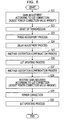
- Fig. 8 is a flowchart illustrating a communication device distortion compensation process.
- the communication device undergoes power training, for example, at the factory before shipping, and transmission powers for specific transmission frequencies are stored in the memory 35. Further, when the power is turned on, the LUT 24e stores the initial values for all the addresses. For example, the LUT 24e stores the distortion compensation coefficient of 1+j ⁇ 0 so that the transmission signals inputted into the multiplier 24a are outputted as is.
- Step S21 The transmission signal generating unit 21 outputs the transmission frequency information of a profile inputted by the user to the correction value calculation unit 36 when, for example, the communication device power is turned on.
- the correction value calculation unit 36 refers to the memory 35 and calculates the pseudo transmission power of the set frequency included in the transmission frequency information.
- the correction value calculation unit 36 calculates the power correction value for the set frequency when the pseudo transmission power is calculated. In other words, the correction value calculation unit 36 calculates the correction value for obtaining the maximum transmission power of the set frequency. The correction value calculation unit 36 outputs the calculated correction value to the SEL 41b.
- the SEL 41b outputs the correction value calculated by the correction value calculation unit 36 to the gain adjusting unit 41c. Although the calculated correction value is outputted to the multiplier 24c, the multiplier 24c does not multiply the correction value by the feedback signal until the power correction step described below is executed.
- the gain adjusting unit 41c multiplies the correction value outputted from the SEL 41b by the distortion compensation coefficient stored in the LUT 24e. Specifically, the gain adjusting unit 41c corrects the distortion compensation coefficient stored in the LUT 24e based on the correction value outputted by the SEL 41b. As a result, the distortion compensation coefficient (power value) is adjusted by the power correction value amount calculated by the correction value calculation unit 36.
- Step S22 The communication device begins sending the user data.
- the transmission signal generating unit 21 outputs the user data to the S/P unit 22.
- the distortion compensation coefficient of the LUT 24e is corrected by the power correction value calculated by the correction value calculation unit 36.
- the power corrected transmission signal is outputted from the multiplier 24a when the user data is outputted from the transmission signal generating unit 21.
- Step S23 The communication device conducts a phase adjustment process.
- the phase adjustment process is conducted to match the phases of the feedback signal and the transmission signal inputted into the LMS calculating unit 24d.
- Step S24 The communication device conducts a delay adjustment process.
- the delay adjustment process is conducted to match the timing of the feedback signal and the transmission signal inputted into the LMS calculating unit 24d.
- Step S25 The communication device conducts another distortion compensation process.
- the communication device conducts a process to remove the DC offset and the like.
- Step S26 The LMS calculating unit 24d updates the LUT 24e.
- Step S27 The communication device conducts another distortion compensation process.
- the communication device conducts the distortion compensation processes described in steps S23 to S25.
- Step S28 The gain adjusting unit 41c restores the distortion compensation coefficient with the correction value amount (power value amount adjusted by the distortion compensation coefficient) multiplied by the distortion compensation coefficient of the LUT 24e.
- the uncorrected distortion compensation coefficient which is updated in step S26 is stored in the LUT 24e.
- the output of the SEL 41b is switched from the correction value of the correction value calculation unit 36 to the gain adjustment value of the LUT gain controlling unit 41a.
- the distortion compensation coefficient of the LUT 24e is gain adjusted based on the power difference between the forward signal measured by the power measuring unit 51 and the feedback signal.
- Step S29 The multiplier 24c outputs the feedback signal with the calculated correction value to the LMS calculating unit 24d.
- Step S30 The LMS calculating unit 24d updates the LUT 24e.
- the transmission signal is multiplied by the distortion compensation coefficient updated in the LUT 24e by the multiplier 24a.
- the communication device then repeats the processes of steps S23 to S26 and the LUT updating process.
- the gain adjusting unit 41c multiplies the correction value calculated by the correction value calculation unit 36 by the distortion compensation coefficient of the LUT 24e before the transmission signal is transmitted after turning on the power of the communication device, and the distortion compensation coefficient of the LUT 24e is restored by the multiplied correction value amount after the distortion compensation coefficient of the LUT 24e is updated. Then, the multiplier 24c multiplies the correction value calculated by the correction value calculation unit 36 by the feedback signal after the distortion compensation coefficient of the LUT 24e is restored with the correction value amount by the gain adjusting unit 41c. As a result, power correction can be reflected in the user data immediately after beginning to transmit the user data.
- the first and second embodiments have been described relating to a communication device that conducts wireless communication.
- a communication device that conducts communication with optical signals may also be applicable.
- a communication device that converts the D/A converted transmission signals to optical signals, amplifies and transmits the signals may be applicable.
- the invention also provides a computer program for carrying out any of the methods described herein.
- a computer program embodying the invention may be stored on a computer-readable medium, or it could, for example, be in the form of a signal such as a downloadable data signal provided from an Internet website, or it could be in any other form.
Landscapes
- Engineering & Computer Science (AREA)
- Physics & Mathematics (AREA)
- Computer Networks & Wireless Communication (AREA)
- Signal Processing (AREA)
- Power Engineering (AREA)
- Electromagnetism (AREA)
- Nonlinear Science (AREA)
- Transmitters (AREA)
- Amplifiers (AREA)
Claims (7)
- Kommunikationsvorrichtung, die operabel ist für Kompensieren einer Verzerrung eines Sendesignals, Verstärken des kompensierten Sendesignals durch einen Verstärker und Ausgabe des verstärkten Signals, wobei die Vorrichtung folgendes aufweist:eine Speichereinheit (4; 35), die operabel ist für Speichern einer Sendecharakteristik einer Sendeleistung der Kommunikationsvorrichtung;eine Korrektureinheit (5), die operabel ist für Berechnen eines Leistungswerts (P') bei einer festgelegten Sendefrequenz (fx; f1) durch Bezugnahme auf die Speichereinheit (4), und für Korrektur eines Rückkopplungssignals des Sendesignals, verstärkt durch den Verstärker auf Basis des berechneten Leistungswerts (P') und einer maximalen Sendeleistung (Pm), die durch die Kommunikationsvorrichtung definiert ist;undeine Berechnungseinheit (6), die operabel ist für Berechnung eines Verzerrungskompensationskoeffizienten auf Basis des Sendesignals und des korrigierten Rückkopplungssignals, dadurch gekennzeichnet, dassdie Korrektureinheit (5) Folgendes aufweist:eine Korrekturwertberechnungseinheit (36), die operabel ist für Erhalten von Leistungswerten (P1, P2) entsprechend zwei Frequenzen (TRf1, TRf2) nahe der festgelegten Sendefrequenz (f1) durch Bezugnahme auf die Speichereinheit (4; 35), Berechnen eines Leistungswerts (P') der festgelegten Sendefrequenz (f1) von einer linearen Näherung der erhaltenen Leistungswerte (P1, P2), und Berechnen einer Differenz zwischen dem berechneten Leistungswerte (P') und der maximalen Sendeleistung (Pm), die durch die Kommunikationsvorrichtung definiert ist; undeinen Multiplikator (24c), der operabel ist für Multiplizieren des Rückkopplungssignals mit der von der Korrekturwertberechnungseinheit (36) berechneten Differenz.
- Kommunikationsvorrichtung nach Anspruch 1, ferner aufweisend:eine Verzerrungskompensationskoeffizienten-Speichereinheit, die operabel ist für Speichern des Verzerrungskompensationskoeffizienten; undeine Einstelleinheit, die operabel ist für, vor dem Senden des Sendesignals bei Einschalten der Kommunikationsvorrichtung, für Multiplizieren der von der Korrekturwertberechnungseinheit (36) berechneten Differenz mit dem in der Verzerrungskompensationskoeffizienten-Speichereinheit gespeicherten Verzerrungskompensationskoeffizienten, und für Wiederherstellung des in der Verzerrungskompensationskoeffizienten-Speichereinheit gespeicherten Verzerrungskompensationskoeffizienten durch die multiplizierte Menge, nachdem der in der Verzerrungskompensationskoeffizienten-Speichereinheit gespeicherte Verzerrungskompensationskoeffizient aktualisiert worden ist,wobei der Multiplikator operabel ist für Multiplizieren des Rückkopplungssignals mit der von der Korrekturwertberechnungseinheit (36) berechneten Differenz, nachdem der in derVerzerrungskompensationskoeffizienten-Speichereinheit gespeicherte Verzerrungskompensationskoeffizient durch die Einstelleinheit wiederhergestellt worden ist.
- Kommunikationsvorrichtung nach einem der vorhergehenden Ansprüche,
wobei die in der Speichereinheit (4; 35) gespeicherten Leistungswerte (P1, P2) den durch gleichmäßiges Teilen eines für die Kommunikationsvorrichtung zur Verfügung stehenden Sendefrequenzbands erhaltenen Frequenzen (TRf1 bis TRf11) Frequenzen entsprechen. - Kommunikationsvorrichtung nach einem der vorhergehenden Ansprüche, ferner aufweisend:eine Übungseinheit (34), die operabel ist für Ändern einer Signalfrequenz, Erhalten eines Leistungswerts eines Sendesignals für jede Frequenz und Speichern des Leistungswerts in der Speichereinheit.
- Kommunikationsvorrichtung nach Anspruch 4, wobei in der Speichereinheit vor der Auslieferung der Kommunikationsvorrichtung durch die Übungseinheit gespeicherte Leistungswerte gespeichert sind.
- Leistungskompensationsverfahren für eine Kommunikationsvorrichtung, wobei die Vorrichtung operabel ist für Kompensieren einer Verzerrung eines Sendesignal, Verstärken des kompensierten Sendesignals durch einen Verstärker und Ausgabe des verstärkten Signals, wobei das Leistungskompensationsverfahren Folgendes aufweist:Bezugnahme auf eine Speichereinheit (4; 35), die Sendeleistungsfrequenzcharakteristik speichert, und Berechnen eines Leistungswerts (P') einer festzulegenden Sendefrequenz, undKorrektur eines Rückkopplungssignals vom Sendesignal, verstärkt durch den Verstärker auf Basis des berechneten Leistungswerts (P') und einer maximalen Leistung (Pm), die durch die Kommunikationsvorrichtung definiert ist; undBerechnen eines Verzerrungskompensationskoeffizienten auf Basis des Sendesignale und des korrigierten Rückkopplungssignals, dadurch gekennzeichnet, dassdie Korrektureinheit Folgendes aufweist:Erhalten von Leistungswerten (P1, P2) entsprechend zwei Frequenzen (TRf1, TRf2) nahe der festgelegten Sendefrequenz (f1) durch Bezugnahme auf die Speichereinheit (4; 35), Berechnen eines Leistungswerts (P') der festgelegten Sendefrequenz (f1) von einer linearen Näherung der erhaltenen Leistungswerte (P1, P2), und Berechnen einer Differenz zwischen dem berechneten Leistungswerte (P') und der maximalen Sendeleistung (Pm), die durch die Kommunikationsvorrichtung definiert ist; undMultiplizieren des Rückkopplungssignals mit der berechneten Differenz.
- Computerprogramm, das, wenn ausgeführt auf einer Kommunikationsvorrichtung, die operabel ist für Kompensieren einer Verzerrung eines Sendesignals, Verstärkung des kompensierten Sendesignals durch einen Verstärker, und für eine Ausgabe des verstärkten Signals, bei der Kommunikationsvorrichtung ein Ausführen des Leistungskompensationsverfahrens nach Anspruch 6 bewirkt.
Applications Claiming Priority (1)
| Application Number | Priority Date | Filing Date | Title |
|---|---|---|---|
| JP2010052534A JP5375683B2 (ja) | 2010-03-10 | 2010-03-10 | 通信装置および電力補正方法 |
Publications (2)
| Publication Number | Publication Date |
|---|---|
| EP2365629A1 EP2365629A1 (de) | 2011-09-14 |
| EP2365629B1 true EP2365629B1 (de) | 2013-09-04 |
Family
ID=44148672
Family Applications (1)
| Application Number | Title | Priority Date | Filing Date |
|---|---|---|---|
| EP11156731.9A Not-in-force EP2365629B1 (de) | 2010-03-10 | 2011-03-03 | Kommunikationsvorrichtung und Leistungskorrekturverfahren |
Country Status (3)
| Country | Link |
|---|---|
| US (1) | US8520772B2 (de) |
| EP (1) | EP2365629B1 (de) |
| JP (1) | JP5375683B2 (de) |
Families Citing this family (14)
| Publication number | Priority date | Publication date | Assignee | Title |
|---|---|---|---|---|
| JP5754899B2 (ja) * | 2009-10-07 | 2015-07-29 | ソニー株式会社 | 復号装置および方法、並びにプログラム |
| JP5850216B2 (ja) | 2010-04-13 | 2016-02-03 | ソニー株式会社 | 信号処理装置および方法、符号化装置および方法、復号装置および方法、並びにプログラム |
| JP5609737B2 (ja) | 2010-04-13 | 2014-10-22 | ソニー株式会社 | 信号処理装置および方法、符号化装置および方法、復号装置および方法、並びにプログラム |
| JP5707842B2 (ja) | 2010-10-15 | 2015-04-30 | ソニー株式会社 | 符号化装置および方法、復号装置および方法、並びにプログラム |
| US8699972B2 (en) | 2011-11-15 | 2014-04-15 | Qualcomm Incorporated | Transmit power calibration in a communication system |
| JP6094071B2 (ja) * | 2012-07-02 | 2017-03-15 | 富士通株式会社 | 歪補償装置及び歪補償方法 |
| JP6035919B2 (ja) * | 2012-07-09 | 2016-11-30 | 富士通株式会社 | 送信装置、及び送信方法 |
| JP6075012B2 (ja) * | 2012-10-31 | 2017-02-08 | 株式会社Jvcケンウッド | 無線機 |
| JP6059003B2 (ja) | 2012-12-26 | 2017-01-11 | パナソニック株式会社 | 歪み補償装置及び歪み補償方法 |
| US20140270291A1 (en) * | 2013-03-15 | 2014-09-18 | Mark C. Flynn | Fitting a Bilateral Hearing Prosthesis System |
| JP6531649B2 (ja) | 2013-09-19 | 2019-06-19 | ソニー株式会社 | 符号化装置および方法、復号化装置および方法、並びにプログラム |
| JP6209925B2 (ja) * | 2013-10-09 | 2017-10-11 | 富士通株式会社 | 歪補償装置および歪補償方法 |
| JP6255917B2 (ja) * | 2013-11-07 | 2018-01-10 | 富士通株式会社 | 無線装置及び無線アクセスシステム |
| KR102356012B1 (ko) | 2013-12-27 | 2022-01-27 | 소니그룹주식회사 | 복호화 장치 및 방법, 및 프로그램 |
Family Cites Families (18)
| Publication number | Priority date | Publication date | Assignee | Title |
|---|---|---|---|---|
| GB2265270B (en) | 1992-03-02 | 1996-06-12 | Motorola Ltd | Rf power amplifier with linearization |
| JP4183364B2 (ja) * | 1999-12-28 | 2008-11-19 | 富士通株式会社 | 歪補償装置 |
| JP2002094394A (ja) * | 2000-09-19 | 2002-03-29 | Matsushita Electric Ind Co Ltd | 送信装置及び送信出力制御方法 |
| JP2002141754A (ja) * | 2000-11-02 | 2002-05-17 | Matsushita Electric Ind Co Ltd | プリディストーション装置 |
| JP3944353B2 (ja) | 2000-11-17 | 2007-07-11 | 株式会社ケンウッド | 増幅器、及び音声出力方法 |
| JP4642272B2 (ja) * | 2001-05-29 | 2011-03-02 | パナソニック株式会社 | 送信出力補正装置 |
| JP3805221B2 (ja) * | 2001-09-18 | 2006-08-02 | 株式会社日立国際電気 | 歪み補償装置 |
| JP3946188B2 (ja) | 2002-12-10 | 2007-07-18 | 株式会社エヌ・ティ・ティ・ドコモ | 線形電力増幅方法、線形電力増幅器及びそのディジタルプリディストータ設定方法 |
| US7170342B2 (en) * | 2002-12-10 | 2007-01-30 | Ntt Docomo, Inc. | Linear power amplification method and linear power amplifier |
| JP2004320185A (ja) | 2003-04-14 | 2004-11-11 | Hitachi Kokusai Electric Inc | 前置歪補償電力増幅装置 |
| JP2004363713A (ja) * | 2003-06-02 | 2004-12-24 | Mitsubishi Electric Corp | 送信装置 |
| JP4371830B2 (ja) | 2004-01-27 | 2009-11-25 | 富士通株式会社 | 歪補償増幅装置および基地局 |
| JP4492246B2 (ja) * | 2004-08-02 | 2010-06-30 | 富士通株式会社 | 歪み補償装置 |
| JP4308163B2 (ja) * | 2005-03-22 | 2009-08-05 | 富士通株式会社 | 歪補償装置 |
| DE602006000525T2 (de) | 2005-06-03 | 2009-02-05 | Ntt Docomo Inc. | Mehrbandvorverzerrer mit Korrekturwertetabellen |
| JP4617265B2 (ja) * | 2006-02-14 | 2011-01-19 | 富士通株式会社 | 歪補償装置及び歪補償方法 |
| JP2007318358A (ja) * | 2006-05-24 | 2007-12-06 | Matsushita Electric Ind Co Ltd | 無線信号送信機 |
| JP5254705B2 (ja) | 2008-08-27 | 2013-08-07 | 株式会社東海理化電機製作所 | プリテンショナ |
-
2010
- 2010-03-10 JP JP2010052534A patent/JP5375683B2/ja not_active Expired - Fee Related
-
2011
- 2011-03-03 US US13/039,765 patent/US8520772B2/en not_active Expired - Fee Related
- 2011-03-03 EP EP11156731.9A patent/EP2365629B1/de not_active Not-in-force
Also Published As
| Publication number | Publication date |
|---|---|
| JP2011188321A (ja) | 2011-09-22 |
| US8520772B2 (en) | 2013-08-27 |
| EP2365629A1 (de) | 2011-09-14 |
| JP5375683B2 (ja) | 2013-12-25 |
| US20110222630A1 (en) | 2011-09-15 |
Similar Documents
| Publication | Publication Date | Title |
|---|---|---|
| EP2365629B1 (de) | Kommunikationsvorrichtung und Leistungskorrekturverfahren | |
| JP5742186B2 (ja) | 増幅装置 | |
| US8437425B2 (en) | Distortion compensation device, distortion compensation method and wireless apparatus | |
| US20040001559A1 (en) | Postdistortion amplifier with predistorted postdistortion | |
| US9584167B2 (en) | Wireless communication system, distortion compensation device, and distortion compensation method | |
| US20180248572A1 (en) | Communication device, communication method, and cancellation device | |
| KR101101596B1 (ko) | 왜곡 보상 장치 및 방법 | |
| US20120224654A1 (en) | Transmitter and distortion compensating method | |
| US20110298536A1 (en) | Distortion compensation amplifier | |
| US7248642B1 (en) | Frequency-dependent phase pre-distortion for reducing spurious emissions in communication networks | |
| EP2262104B1 (de) | Vorrichtung zur drahtlosen Kommunikation | |
| US8755757B2 (en) | Amplifier apparatus, radio transmitting apparatus including same, and method of adjusting gain of amplifier apparatus | |
| JP2005151119A (ja) | 歪補償装置 | |
| JP3268135B2 (ja) | 無線機 | |
| JP2018195955A (ja) | 無線通信装置及び歪み補償方法 | |
| US20110124304A1 (en) | Transmission apparatus and adjustment value measurement method | |
| JP5434818B2 (ja) | 歪補償装置、歪補償方法及び無線通信装置 | |
| US20130051492A1 (en) | Apparatus and method for operating a transmitter | |
| US8311493B2 (en) | Radio apparatus, distortion correction device, and distortion correction method | |
| EP1511180B1 (de) | Verzerrungskompensator | |
| US11424774B2 (en) | Wireless communication apparatus and coefficient updating method | |
| US11196537B2 (en) | Wireless communication apparatus and coefficient update method | |
| US20180054170A1 (en) | Distortion compensation device and coefficient update method | |
| US20060029154A1 (en) | Distortion compensation device and distortion compensation method | |
| JP2011244087A (ja) | 基地局及び基地局での送信信号の調整方法 |
Legal Events
| Date | Code | Title | Description |
|---|---|---|---|
| PUAI | Public reference made under article 153(3) epc to a published international application that has entered the european phase |
Free format text: ORIGINAL CODE: 0009012 |
|
| AK | Designated contracting states |
Kind code of ref document: A1 Designated state(s): AL AT BE BG CH CY CZ DE DK EE ES FI FR GB GR HR HU IE IS IT LI LT LU LV MC MK MT NL NO PL PT RO RS SE SI SK SM TR |
|
| AX | Request for extension of the european patent |
Extension state: BA ME |
|
| 17P | Request for examination filed |
Effective date: 20120312 |
|
| GRAP | Despatch of communication of intention to grant a patent |
Free format text: ORIGINAL CODE: EPIDOSNIGR1 |
|
| RIC1 | Information provided on ipc code assigned before grant |
Ipc: H04W 52/22 20090101ALI20130308BHEP Ipc: H03F 1/32 20060101AFI20130308BHEP Ipc: H04B 17/00 20060101ALI20130308BHEP Ipc: H03F 3/24 20060101ALI20130308BHEP Ipc: H04B 1/04 20060101ALI20130308BHEP |
|
| INTG | Intention to grant announced |
Effective date: 20130326 |
|
| GRAS | Grant fee paid |
Free format text: ORIGINAL CODE: EPIDOSNIGR3 |
|
| GRAA | (expected) grant |
Free format text: ORIGINAL CODE: 0009210 |
|
| AK | Designated contracting states |
Kind code of ref document: B1 Designated state(s): AL AT BE BG CH CY CZ DE DK EE ES FI FR GB GR HR HU IE IS IT LI LT LU LV MC MK MT NL NO PL PT RO RS SE SI SK SM TR |
|
| REG | Reference to a national code |
Ref country code: GB Ref legal event code: FG4D |
|
| REG | Reference to a national code |
Ref country code: CH Ref legal event code: EP |
|
| REG | Reference to a national code |
Ref country code: AT Ref legal event code: REF Ref document number: 630963 Country of ref document: AT Kind code of ref document: T Effective date: 20130915 |
|
| REG | Reference to a national code |
Ref country code: IE Ref legal event code: FG4D |
|
| REG | Reference to a national code |
Ref country code: DE Ref legal event code: R096 Ref document number: 602011002876 Country of ref document: DE Effective date: 20131024 |
|
| REG | Reference to a national code |
Ref country code: AT Ref legal event code: MK05 Ref document number: 630963 Country of ref document: AT Kind code of ref document: T Effective date: 20130904 |
|
| REG | Reference to a national code |
Ref country code: NL Ref legal event code: VDEP Effective date: 20130904 |
|
| PG25 | Lapsed in a contracting state [announced via postgrant information from national office to epo] |
Ref country code: NO Free format text: LAPSE BECAUSE OF FAILURE TO SUBMIT A TRANSLATION OF THE DESCRIPTION OR TO PAY THE FEE WITHIN THE PRESCRIBED TIME-LIMIT Effective date: 20131204 Ref country code: SE Free format text: LAPSE BECAUSE OF FAILURE TO SUBMIT A TRANSLATION OF THE DESCRIPTION OR TO PAY THE FEE WITHIN THE PRESCRIBED TIME-LIMIT Effective date: 20130904 Ref country code: AT Free format text: LAPSE BECAUSE OF FAILURE TO SUBMIT A TRANSLATION OF THE DESCRIPTION OR TO PAY THE FEE WITHIN THE PRESCRIBED TIME-LIMIT Effective date: 20130904 Ref country code: HR Free format text: LAPSE BECAUSE OF FAILURE TO SUBMIT A TRANSLATION OF THE DESCRIPTION OR TO PAY THE FEE WITHIN THE PRESCRIBED TIME-LIMIT Effective date: 20130904 Ref country code: CY Free format text: LAPSE BECAUSE OF FAILURE TO SUBMIT A TRANSLATION OF THE DESCRIPTION OR TO PAY THE FEE WITHIN THE PRESCRIBED TIME-LIMIT Effective date: 20130619 Ref country code: LT Free format text: LAPSE BECAUSE OF FAILURE TO SUBMIT A TRANSLATION OF THE DESCRIPTION OR TO PAY THE FEE WITHIN THE PRESCRIBED TIME-LIMIT Effective date: 20130904 |
|
| REG | Reference to a national code |
Ref country code: NL Ref legal event code: VDEP Effective date: 20130904 |
|
| REG | Reference to a national code |
Ref country code: LT Ref legal event code: MG4D |
|
| PG25 | Lapsed in a contracting state [announced via postgrant information from national office to epo] |
Ref country code: FI Free format text: LAPSE BECAUSE OF FAILURE TO SUBMIT A TRANSLATION OF THE DESCRIPTION OR TO PAY THE FEE WITHIN THE PRESCRIBED TIME-LIMIT Effective date: 20130904 Ref country code: LV Free format text: LAPSE BECAUSE OF FAILURE TO SUBMIT A TRANSLATION OF THE DESCRIPTION OR TO PAY THE FEE WITHIN THE PRESCRIBED TIME-LIMIT Effective date: 20130904 Ref country code: GR Free format text: LAPSE BECAUSE OF FAILURE TO SUBMIT A TRANSLATION OF THE DESCRIPTION OR TO PAY THE FEE WITHIN THE PRESCRIBED TIME-LIMIT Effective date: 20131205 Ref country code: PL Free format text: LAPSE BECAUSE OF FAILURE TO SUBMIT A TRANSLATION OF THE DESCRIPTION OR TO PAY THE FEE WITHIN THE PRESCRIBED TIME-LIMIT Effective date: 20130904 Ref country code: SI Free format text: LAPSE BECAUSE OF FAILURE TO SUBMIT A TRANSLATION OF THE DESCRIPTION OR TO PAY THE FEE WITHIN THE PRESCRIBED TIME-LIMIT Effective date: 20130904 |
|
| PG25 | Lapsed in a contracting state [announced via postgrant information from national office to epo] |
Ref country code: CY Free format text: LAPSE BECAUSE OF FAILURE TO SUBMIT A TRANSLATION OF THE DESCRIPTION OR TO PAY THE FEE WITHIN THE PRESCRIBED TIME-LIMIT Effective date: 20130904 Ref country code: BE Free format text: LAPSE BECAUSE OF FAILURE TO SUBMIT A TRANSLATION OF THE DESCRIPTION OR TO PAY THE FEE WITHIN THE PRESCRIBED TIME-LIMIT Effective date: 20130904 |
|
| PG25 | Lapsed in a contracting state [announced via postgrant information from national office to epo] |
Ref country code: EE Free format text: LAPSE BECAUSE OF FAILURE TO SUBMIT A TRANSLATION OF THE DESCRIPTION OR TO PAY THE FEE WITHIN THE PRESCRIBED TIME-LIMIT Effective date: 20130904 Ref country code: IS Free format text: LAPSE BECAUSE OF FAILURE TO SUBMIT A TRANSLATION OF THE DESCRIPTION OR TO PAY THE FEE WITHIN THE PRESCRIBED TIME-LIMIT Effective date: 20140104 Ref country code: NL Free format text: LAPSE BECAUSE OF FAILURE TO SUBMIT A TRANSLATION OF THE DESCRIPTION OR TO PAY THE FEE WITHIN THE PRESCRIBED TIME-LIMIT Effective date: 20130904 Ref country code: RO Free format text: LAPSE BECAUSE OF FAILURE TO SUBMIT A TRANSLATION OF THE DESCRIPTION OR TO PAY THE FEE WITHIN THE PRESCRIBED TIME-LIMIT Effective date: 20130904 Ref country code: SK Free format text: LAPSE BECAUSE OF FAILURE TO SUBMIT A TRANSLATION OF THE DESCRIPTION OR TO PAY THE FEE WITHIN THE PRESCRIBED TIME-LIMIT Effective date: 20130904 Ref country code: CZ Free format text: LAPSE BECAUSE OF FAILURE TO SUBMIT A TRANSLATION OF THE DESCRIPTION OR TO PAY THE FEE WITHIN THE PRESCRIBED TIME-LIMIT Effective date: 20130904 |
|
| PG25 | Lapsed in a contracting state [announced via postgrant information from national office to epo] |
Ref country code: ES Free format text: LAPSE BECAUSE OF FAILURE TO SUBMIT A TRANSLATION OF THE DESCRIPTION OR TO PAY THE FEE WITHIN THE PRESCRIBED TIME-LIMIT Effective date: 20130904 |
|
| REG | Reference to a national code |
Ref country code: DE Ref legal event code: R097 Ref document number: 602011002876 Country of ref document: DE |
|
| PG25 | Lapsed in a contracting state [announced via postgrant information from national office to epo] |
Ref country code: PT Free format text: LAPSE BECAUSE OF FAILURE TO SUBMIT A TRANSLATION OF THE DESCRIPTION OR TO PAY THE FEE WITHIN THE PRESCRIBED TIME-LIMIT Effective date: 20140106 |
|
| PLBE | No opposition filed within time limit |
Free format text: ORIGINAL CODE: 0009261 |
|
| STAA | Information on the status of an ep patent application or granted ep patent |
Free format text: STATUS: NO OPPOSITION FILED WITHIN TIME LIMIT |
|
| 26N | No opposition filed |
Effective date: 20140605 |
|
| PG25 | Lapsed in a contracting state [announced via postgrant information from national office to epo] |
Ref country code: IT Free format text: LAPSE BECAUSE OF FAILURE TO SUBMIT A TRANSLATION OF THE DESCRIPTION OR TO PAY THE FEE WITHIN THE PRESCRIBED TIME-LIMIT Effective date: 20130904 |
|
| REG | Reference to a national code |
Ref country code: DE Ref legal event code: R097 Ref document number: 602011002876 Country of ref document: DE Effective date: 20140605 |
|
| PG25 | Lapsed in a contracting state [announced via postgrant information from national office to epo] |
Ref country code: DK Free format text: LAPSE BECAUSE OF FAILURE TO SUBMIT A TRANSLATION OF THE DESCRIPTION OR TO PAY THE FEE WITHIN THE PRESCRIBED TIME-LIMIT Effective date: 20130904 |
|
| PG25 | Lapsed in a contracting state [announced via postgrant information from national office to epo] |
Ref country code: LU Free format text: LAPSE BECAUSE OF FAILURE TO SUBMIT A TRANSLATION OF THE DESCRIPTION OR TO PAY THE FEE WITHIN THE PRESCRIBED TIME-LIMIT Effective date: 20140303 |
|
| REG | Reference to a national code |
Ref country code: CH Ref legal event code: PL |
|
| REG | Reference to a national code |
Ref country code: IE Ref legal event code: MM4A |
|
| PG25 | Lapsed in a contracting state [announced via postgrant information from national office to epo] |
Ref country code: CH Free format text: LAPSE BECAUSE OF NON-PAYMENT OF DUE FEES Effective date: 20140331 Ref country code: LI Free format text: LAPSE BECAUSE OF NON-PAYMENT OF DUE FEES Effective date: 20140331 Ref country code: IE Free format text: LAPSE BECAUSE OF NON-PAYMENT OF DUE FEES Effective date: 20140303 |
|
| REG | Reference to a national code |
Ref country code: FR Ref legal event code: PLFP Year of fee payment: 6 |
|
| PG25 | Lapsed in a contracting state [announced via postgrant information from national office to epo] |
Ref country code: MT Free format text: LAPSE BECAUSE OF FAILURE TO SUBMIT A TRANSLATION OF THE DESCRIPTION OR TO PAY THE FEE WITHIN THE PRESCRIBED TIME-LIMIT Effective date: 20130904 |
|
| PG25 | Lapsed in a contracting state [announced via postgrant information from national office to epo] |
Ref country code: SM Free format text: LAPSE BECAUSE OF FAILURE TO SUBMIT A TRANSLATION OF THE DESCRIPTION OR TO PAY THE FEE WITHIN THE PRESCRIBED TIME-LIMIT Effective date: 20130904 |
|
| PG25 | Lapsed in a contracting state [announced via postgrant information from national office to epo] |
Ref country code: MC Free format text: LAPSE BECAUSE OF FAILURE TO SUBMIT A TRANSLATION OF THE DESCRIPTION OR TO PAY THE FEE WITHIN THE PRESCRIBED TIME-LIMIT Effective date: 20130904 |
|
| PG25 | Lapsed in a contracting state [announced via postgrant information from national office to epo] |
Ref country code: RS Free format text: LAPSE BECAUSE OF FAILURE TO SUBMIT A TRANSLATION OF THE DESCRIPTION OR TO PAY THE FEE WITHIN THE PRESCRIBED TIME-LIMIT Effective date: 20130904 Ref country code: BG Free format text: LAPSE BECAUSE OF FAILURE TO SUBMIT A TRANSLATION OF THE DESCRIPTION OR TO PAY THE FEE WITHIN THE PRESCRIBED TIME-LIMIT Effective date: 20130904 |
|
| PG25 | Lapsed in a contracting state [announced via postgrant information from national office to epo] |
Ref country code: TR Free format text: LAPSE BECAUSE OF FAILURE TO SUBMIT A TRANSLATION OF THE DESCRIPTION OR TO PAY THE FEE WITHIN THE PRESCRIBED TIME-LIMIT Effective date: 20130904 Ref country code: HU Free format text: LAPSE BECAUSE OF FAILURE TO SUBMIT A TRANSLATION OF THE DESCRIPTION OR TO PAY THE FEE WITHIN THE PRESCRIBED TIME-LIMIT; INVALID AB INITIO Effective date: 20110303 |
|
| REG | Reference to a national code |
Ref country code: FR Ref legal event code: PLFP Year of fee payment: 7 |
|
| PGFP | Annual fee paid to national office [announced via postgrant information from national office to epo] |
Ref country code: DE Payment date: 20170228 Year of fee payment: 7 Ref country code: FR Payment date: 20170213 Year of fee payment: 7 |
|
| PGFP | Annual fee paid to national office [announced via postgrant information from national office to epo] |
Ref country code: GB Payment date: 20170301 Year of fee payment: 7 |
|
| PG25 | Lapsed in a contracting state [announced via postgrant information from national office to epo] |
Ref country code: MK Free format text: LAPSE BECAUSE OF FAILURE TO SUBMIT A TRANSLATION OF THE DESCRIPTION OR TO PAY THE FEE WITHIN THE PRESCRIBED TIME-LIMIT Effective date: 20130904 |
|
| REG | Reference to a national code |
Ref country code: DE Ref legal event code: R119 Ref document number: 602011002876 Country of ref document: DE |
|
| PG25 | Lapsed in a contracting state [announced via postgrant information from national office to epo] |
Ref country code: AL Free format text: LAPSE BECAUSE OF FAILURE TO SUBMIT A TRANSLATION OF THE DESCRIPTION OR TO PAY THE FEE WITHIN THE PRESCRIBED TIME-LIMIT Effective date: 20130904 |
|
| GBPC | Gb: european patent ceased through non-payment of renewal fee |
Effective date: 20180303 |
|
| PG25 | Lapsed in a contracting state [announced via postgrant information from national office to epo] |
Ref country code: DE Free format text: LAPSE BECAUSE OF NON-PAYMENT OF DUE FEES Effective date: 20181002 |
|
| PG25 | Lapsed in a contracting state [announced via postgrant information from national office to epo] |
Ref country code: GB Free format text: LAPSE BECAUSE OF NON-PAYMENT OF DUE FEES Effective date: 20180303 |
|
| PG25 | Lapsed in a contracting state [announced via postgrant information from national office to epo] |
Ref country code: FR Free format text: LAPSE BECAUSE OF NON-PAYMENT OF DUE FEES Effective date: 20180331 |