EP2365634B1 - Procédé et appareil de modulation de densité d' impulsions - Google Patents
Procédé et appareil de modulation de densité d' impulsions Download PDFInfo
- Publication number
- EP2365634B1 EP2365634B1 EP10156140.5A EP10156140A EP2365634B1 EP 2365634 B1 EP2365634 B1 EP 2365634B1 EP 10156140 A EP10156140 A EP 10156140A EP 2365634 B1 EP2365634 B1 EP 2365634B1
- Authority
- EP
- European Patent Office
- Prior art keywords
- pdm
- stream
- input
- control
- switch
- Prior art date
- Legal status (The legal status is an assumption and is not a legal conclusion. Google has not performed a legal analysis and makes no representation as to the accuracy of the status listed.)
- Active
Links
Images


Classifications
-
- H—ELECTRICITY
- H03—ELECTRONIC CIRCUITRY
- H03M—CODING; DECODING; CODE CONVERSION IN GENERAL
- H03M3/00—Conversion of analogue values to or from differential modulation
- H03M3/30—Delta-sigma modulation
- H03M3/322—Continuously compensating for, or preventing, undesired influence of physical parameters
- H03M3/368—Continuously compensating for, or preventing, undesired influence of physical parameters of noise other than the quantisation noise already being shaped inherently by delta-sigma modulators
- H03M3/376—Prevention or reduction of switching transients, e.g. glitches
-
- H—ELECTRICITY
- H03—ELECTRONIC CIRCUITRY
- H03M—CODING; DECODING; CODE CONVERSION IN GENERAL
- H03M3/00—Conversion of analogue values to or from differential modulation
- H03M3/30—Delta-sigma modulation
- H03M3/50—Digital/analogue converters using delta-sigma modulation as an intermediate step
Definitions
- the invention relates to apparatus using pulse density modulation and methods of operation.
- Audio amplifiers with a digital input interface are now available. Such audio amplifiers with a digital input instead of an analog input can be more robust against disturbances.
- CMOS90 complementary metal-oxide-semiconductor
- a one-bit pulse density modulation (PDM) stream may originate from a one-bit sigma-delta converter, in an audio processor, which can be relatively inexpensive.
- PDM pulse density modulation
- a good example of a PDM stream is the direct stream digital (DSD) stream used in super audio applications (SACD). This stream is a 64 times over-sampled one-bit PDM stream.
- DSD direct stream digital
- SACD super audio applications
- US 4,142,066 teaches a method an apparatus for encoding speech in which periods of silence are coded using predetermined silence sequences.
- US2002/0025010 describes a circuit for detecting zero values in a one-bit digital signal.
- JP2005123784 describes a signal processor for audio-visual apparatus, wherein the output of a delta-sigma modulated signal is interrupted if integral and average values are equal.
- the processor integrates the delta - sigma modulated signal if signal instructing audio mute ON is obtained.
- the average value is taken for 256 samples of integral value.
- the output of the modulating signal is interrupted if integral and the average values are equal.
- both the first and second integrals are low to provide further reduced audibility.
- the invention relates to an apparatus according to claim 7.
- Figure 1 shows the setup of an audio processor 2 incorporating an interpolation filter and a sigma-delta module 4 providing data along a PDM interface bus 6 consisting of only two wires, a clock wire 8 and a data wire 10.
- the digital data is used to drive amplifier 12 which in turn drives a loudspeaker 14.
- the audio processor 2 needs to be able to send control signals, and these are sent over the same two wires of the bus 6. This cancels the need for extra control bus lines.
- a special pattern of bits is injected in the PDM stream as a control signal to instruct a corresponding function at the amplifier side.
- An example of a control pattern is a repetitive 11001100 (0xCC) pattern which is used to set the amplifier in mute. The audio content of this pattern is zero at low frequencies ( ⁇ 20 kHz). There are a number of different patterns which are possible with zero audio content. Different repetitive patterns can be recognized by the amplifier 12 - these different patterns are used to signal different control signals.
- the control signal may also be referred to as a control stream.
- One possible simple solution would be to store some samples at the amplifier side, which is equal to the length of the control pattern.
- the repetitive pattern needs to be sufficiently long to prevent false triggering because the PDM stream sometimes generates the same pattern as the tokens.
- the length of the repetitive patterns should therefore be long enough to reduce the chance of false triggering.
- a suitable length of time is about 666 ⁇ s, which corresponds to 512 repetitions of the 0x66 pattern if the clock input equals 6.144 MHz.
- storing the samples in the amplifier before sending them to drive the speaker is not really a good solution, since this introduces latency which is too long for some other applications, such as noise cancellation. Storing all the samples requires also extra silicon area.
- the method instead selects the right moment in time to inject the repetitive pattern at the right moment in time, the right moment being when the PDM has no audio content.
- Figure 2 shows the spike in the output analog audio signal (in V) caused by injecting a repetitive pattern using a method according to the invention.
- the audio signal has a spike of about 1 mV in this example. This may be compared to the comparative example of Figure 3 where a repetitive pattern is injected without waiting for a suitable time - in this case the introduction generates a spike about twenty times higher, i.e. about 20mV.
- FIG. 4 shows a block diagram of the circuit in the audio processor 2 used to inject a token.
- the circuit has three inputs, a circuit PDM input 30 accepting a PDM stream, a circuit token input 32 accepting a stream of tokens, and a circuit command input 34 accepting a signal selecting between the PDM and the token streams.
- Switch 36 is used to switch between the streams, and it has a switch PDM input 38 connected to the circuit PDM input 30, a switch token input 40 connected to the circuit token input 32, and two control inputs, namely an inject token control input 42 and an inject PDM control input 44.
- a signal on a control input 42,44 causes the switch to provide the respective signal on output 46.
- the switch outputs the signal on switch token input 40 to output 46.
- the switch 36 outputs the signal on switch PDM input 38 to output 46.
- Command logic (48,50,56) is used to control the switch 36.
- the timing of the switch between the PDM and token streams is moderated by the command logic which includes two additional control units, a token inject control unit 48 with its output connected to the inject token control input 42 of the switch 36, and a PDM inject control unit 50 with its output connected to the inject PDM control input 44.
- Each of the additional control units has a stream input 52 connected to the circuit PDM control input 30 or the circuit token control input 32 and a command input 54 connected to the circuit command input 34.
- the command input 54 of the PDM control unit 50 is connected to the circuit command input 34 via an inverter 56, whereas the command input 54 of the token inject control unit 48 is connected directly to the circuit command input 34.
- the inverter 56 may be omitted and replaced with modified logic inside one or both of the additional control units.
- FIG. 5 illustrates the token inject control unit 48.
- a first integrator 58 with input connected to the stream input 52 and a second integrator 60 connected to the first integrator 58.
- the first integrator 58 calculates the first integral of the PDM stream and the second integrator 60 calculates the second integral.
- both integrators 58, 60 are made up of an adder 64, a limiter 66 and a delay 68.
- Limiter 66 rejects the initial value of the first and second integral. If this initial is not rejected the integrals can have an offset, which can give a false triggering.
- the limiter limits the value to +1, 0 or -1.
- Logic 62 is provided to check when both integrals are zero and the PDM is 1 at the same time as an appropriate input on command input 54. At this point, the token inject control unit 48 outputs a signal to the token control input 42 of switch 36 which causes the token signal from circuit token input 32 to be to be injected and provided on output 46.
- the logic includes a one-detector for detecting a one in the PDM stream, and two zero detectors for detecting a zero output, one zero detector being provided for each integrator. The outputs of the one-detector and the two zero-detectors are put through a multiple input AND gate to output the signal on output 46.
- FIG. 6 shows the PDM inject control unit 50, which is used to switch back to the PDM stream.
- a single integrator 58 is used with the same features of an adder 64, a limiter 66 and a delay 68.
- the output of the integrator 58 is taken through logic 62 in the form of a zero detector.
- the output of the zero detector is combined with the command on the command input with an AND gate to provide the output.
- the audio processor only switches from PDM to token outputs when the first and second integrals of the signal on the PDM stream are zero and the PDM stream 1.
- the audio only switches from token to PDM outputs when the first integral of the signal on the token stream is zero.
- one integrator gives significant reduction in the audibility of a pop or click when switching streams and two two integrators are usually sufficient to provide only a hardly audible click.
- either control unit may include one or two integrators.
- a third integral of the PDM stream is also taken and used to select the correct moment. In this case, all three of the first, second and third integrals of the PDM stream are zero before injecting the token. This further reduces the audibility of any pop or click.
- the embodiments described above limit the output of the integrators to +1, 0 or-1 and the embdoments select for a zero in the integrals.
- the integration may be carried out with more bits.
- Such embodiments may select for a first integral having a modulus less than a first predetermined value and a second integral having a modulus less than a second predetermined value.
- the predetermined values can be selected based on the application to ensure that the period of waiting before a token is transmitted is appropriate.
- a general purpose computer is programmed to carry out the method as described above, namely to process a PDM stream by identifying when the first and second integrals of the PDM stream are zero before introducing a control token.
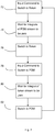
- a computer program product contains code to carry out the steps of a method as shown in Figure 7 .
- a PDM stream is output until a command is received to switch to the control stream (step 72).
- the program waits until the first and second integrals of the PDM stream are low, or in the specific embodiment, zero.
- the method switches to output the control stream.
- the method waits for a command to switch back to the PDM stream (step 78), waits for the first integral of the token stream to be zero (step 80), and then switches back (step 82).
- the method and apparatus are used in class D audio applications.
- the method and apparatus may also be used in combination with mobile telephones.
Landscapes
- Engineering & Computer Science (AREA)
- Theoretical Computer Science (AREA)
- Compression, Expansion, Code Conversion, And Decoders (AREA)
- Amplifiers (AREA)
Claims (12)
- Procédé d'exploitation d'un circuit de sortie de modulation de densité d'impulsions, PDM, comprenant les étapes suivantes :délivrer en sortie un flux de PDM ;commuter pour délivrer en sortie un flux de commande lorsque la première intégrale du flux de PDM a une grandeur inférieure ou égale à une première valeur prédéterminée,caractérisé en ce quel'étape de commutation pour délivrer en sortie un flux de commande est exécutée lorsque la première intégrale du flux de PDM a une grandeur inférieure ou égale à une première valeur prédéterminée et la seconde intégrale du flux de PDM a une grandeur inférieure ou égale à une seconde valeur prédéterminée.
- Procédé selon la revendication 1, dans lequel la ou chaque valeur prédéterminée est égale à zéro.
- Procédé selon la revendication 1 ou la revendication 2, comprenant en outre de revenir sur la commutation pour délivrer en sortie un flux de PDM lorsque la première intégrale du flux de commande a une grandeur inférieure ou égale à la première valeur prédéterminée.
- Produit programme informatique, comprenant un code de programme informatique arrangé pour exécuter les étapes d'un procédé selon l'une quelconque des revendications précédentes lorsqu'il est exécuté sur un ordinateur.
- Produit programme informatique selon la revendication 4 enregistré sur un support de données.
- Appareil de modulation de densité d'impulsions, PDM, comprenant :un commutateur (36) arrangé pour commuter entre un flux de PDM et un flux de commande ; etune logique de commande (48, 50, 56) arrangée pour commander le commutateur (36) pour passer du flux de modulation de densité d'impulsions au flux de commande lorsque la première intégrale du flux de PDM a une grandeur inférieure ou égale à une première valeur prédéterminée,caractérisé en ce quela logique de commande (48, 50, 56) est arrangée pour passer du flux de modulation de densité d'impulsions au flux de commande lorsque la première intégrale du flux de PDM a une grandeur inférieure ou égale à une première valeur prédéterminée et la seconde intégrale du flux de PDM a une grandeur inférieure ou égale à une seconde valeur prédéterminée.
- Appareil de PDM selon la revendication 6, dans lequel les première et seconde valeurs prédéterminées sont égales à zéro.
- Appareil de PDM selon la revendication 6 ou la revendication 7, comprenant :une entrée de PDM de circuit (30) connectée au commutateur (36) et à la logique de commande (48, 50, 56) pour accepter le flux de PDM ;une entrée de jeton de circuit (32) connectée au commutateur (36) et à la logique de commande (48, 50, 56) pour recevoir le flux de commande ;une entrée de commande (34) connectée à la logique de commande (48, 50, 56) pour commander la logique de commande.
- Appareil de PDM selon la revendication 8, dans lequel la logique de commande (48, 50, 56) comprend :une unité de commande d'injection de PDM (50) ayant une entrée de flux d'unité (52) connectée à l'entrée de jeton de circuit (32) et une entrée de commande d'unité (54) connectée à l'entrée de commande (34) arrangée pour délivrer en sortie un signal au commutateur (36) pour commuter vers le flux de modulation de densité d'impulsions à partir du profil de commande lorsque la première intégrale du flux de commande a une grandeur inférieure ou égale à une première valeur prédéterminée ; etune unité de commande d'injection de jeton (48) ayant une entrée de flux d'unité (52) connectée à l'entrée de PDM de circuit (30) et une entrée de commande d'unité (54) connectée à l'entrée de commande (34) arrangée pour délivrer en sortie un signal au commutateur (36) pour commuter vers le profil de commande à partir du flux de modulation de densité d'impulsions lorsque la première intégrale du flux de PDM a une grandeur inférieure ou égale à une première valeur prédéterminée et la seconde intégrale du flux de PDM a une grandeur inférieure ou égale à une seconde valeur prédéterminée.
- Appareil de PDM selon la revendication 9, dans lequel :la logique de commande comprend en outre un inverseur (56) ;l'entrée de commande d'unité (54) d'exactement une unité parmi l'unité de commande d'injection de PDM (48) et l'unité de commande d'injection de jeton (50) est connectée à l'entrée de commande (34) par l'intermédiaire de l'inverseur (56) ; etl'entrée de commande d'unité (54) de l'autre unité parmi l'unité de commande d'injection de PDM (48) et l'unité de commande d'injection de jeton (50) est connectée directement à l'entrée de commande (34).
- Appareil de PDM selon la revendication 9 ou la revendication 10, dans lequel chaque unité parmi l'unité de commande d'injection de PDM (48) et l'unité de commande d'injection de jeton (50) comprend un premier intégrateur (58) connecté à l'entrée de PDM de l'unité (52), un second intégrateur (60) connecté au premier intégrateur (58), et une logique (62) connectée au premier intégrateur (58), au second intégrateur (60) et à l'entrée de commande d'unité (54).
- Appareil de PDM selon la revendication 11, dans lequel chaque intégrateur parmi le premier intégrateur (58) et le second intégrateur (60) comprend un additionneur (64), un limiteur (66) connecté à la sortie de l'additionneur, et une unité de retard (68) arrangée pour renvoyer le signal depuis le limiteur (66) vers l'additionneur (64) avec un retard.
Priority Applications (3)
| Application Number | Priority Date | Filing Date | Title |
|---|---|---|---|
| EP10156140.5A EP2365634B1 (fr) | 2010-03-10 | 2010-03-10 | Procédé et appareil de modulation de densité d' impulsions |
| CN2011100582846A CN102195622A (zh) | 2010-03-10 | 2011-03-08 | 脉冲密度调制方法和装置 |
| US13/044,300 US8681853B2 (en) | 2010-03-10 | 2011-03-09 | Pulse density modulation method and apparatus |
Applications Claiming Priority (1)
| Application Number | Priority Date | Filing Date | Title |
|---|---|---|---|
| EP10156140.5A EP2365634B1 (fr) | 2010-03-10 | 2010-03-10 | Procédé et appareil de modulation de densité d' impulsions |
Publications (2)
| Publication Number | Publication Date |
|---|---|
| EP2365634A1 EP2365634A1 (fr) | 2011-09-14 |
| EP2365634B1 true EP2365634B1 (fr) | 2016-12-21 |
Family
ID=42312883
Family Applications (1)
| Application Number | Title | Priority Date | Filing Date |
|---|---|---|---|
| EP10156140.5A Active EP2365634B1 (fr) | 2010-03-10 | 2010-03-10 | Procédé et appareil de modulation de densité d' impulsions |
Country Status (3)
| Country | Link |
|---|---|
| US (1) | US8681853B2 (fr) |
| EP (1) | EP2365634B1 (fr) |
| CN (1) | CN102195622A (fr) |
Families Citing this family (4)
| Publication number | Priority date | Publication date | Assignee | Title |
|---|---|---|---|---|
| US9871530B1 (en) * | 2016-12-11 | 2018-01-16 | John Howard La Grou | Multi-path analog-to-digital and digital-to-analog conversion of PDM signals |
| US10306348B2 (en) * | 2017-02-16 | 2019-05-28 | Qualcomm Incorporated | Mute pattern injection for a pulse-density modulation microphone |
| CN106849955B (zh) | 2017-03-30 | 2023-10-31 | 绍兴市上虞区幻想动力机器人科技有限公司 | 一种脉冲密度调制方法及脉冲密度值信号转换电路 |
| DE112021005184T5 (de) * | 2020-10-01 | 2023-07-13 | Analog Devices, Inc. | Hilfskommunikation über eine pulsdichtenmodulierte Schnittstelle |
Citations (2)
| Publication number | Priority date | Publication date | Assignee | Title |
|---|---|---|---|---|
| JP2005123784A (ja) * | 2003-10-15 | 2005-05-12 | Sony Corp | 信号処理装置、信号処理方法 |
| US20050213669A1 (en) * | 2004-03-24 | 2005-09-29 | Sony Corporation | Digital signal processing apparatus and digital signal processing method |
Family Cites Families (9)
| Publication number | Priority date | Publication date | Assignee | Title |
|---|---|---|---|---|
| US4142066A (en) * | 1977-12-27 | 1979-02-27 | Bell Telephone Laboratories, Incorporated | Suppression of idle channel noise in delta modulation systems |
| CN1032889C (zh) * | 1992-03-18 | 1996-09-25 | 汤姆森电子用品公司 | 自动环路控制的方法和装置 |
| JP2002076899A (ja) * | 2000-08-29 | 2002-03-15 | Nippon Precision Circuits Inc | ゼロ値検出回路 |
| JP4568572B2 (ja) * | 2004-10-07 | 2010-10-27 | ローム株式会社 | 音声信号出力回路、および音声出力を発生する電子機器 |
| US7283012B2 (en) * | 2005-04-15 | 2007-10-16 | Via Telecom., Ltd. | Tri-state pulse density modulator |
| US7612608B2 (en) * | 2006-08-16 | 2009-11-03 | Intrinsix Corporation | Sigma-delta based Class D audio or servo amplifier with load noise shaping |
| KR100810853B1 (ko) * | 2006-08-25 | 2008-03-06 | 삼성전자주식회사 | 오디오 출력장치에서 팝 노이즈를 방지하기 위한 장치 및방법 |
| US8022756B2 (en) * | 2007-05-15 | 2011-09-20 | Qualcomm, Incorporated | Output circuits with class D amplifier |
| ITMI20080930A1 (it) * | 2008-05-21 | 2009-11-22 | St Microelectronics Srl | Circuito di amplificazione per il pilotaggio di un diffusore |
-
2010
- 2010-03-10 EP EP10156140.5A patent/EP2365634B1/fr active Active
-
2011
- 2011-03-08 CN CN2011100582846A patent/CN102195622A/zh active Pending
- 2011-03-09 US US13/044,300 patent/US8681853B2/en active Active
Patent Citations (2)
| Publication number | Priority date | Publication date | Assignee | Title |
|---|---|---|---|---|
| JP2005123784A (ja) * | 2003-10-15 | 2005-05-12 | Sony Corp | 信号処理装置、信号処理方法 |
| US20050213669A1 (en) * | 2004-03-24 | 2005-09-29 | Sony Corporation | Digital signal processing apparatus and digital signal processing method |
Also Published As
| Publication number | Publication date |
|---|---|
| US8681853B2 (en) | 2014-03-25 |
| CN102195622A (zh) | 2011-09-21 |
| US20110221540A1 (en) | 2011-09-15 |
| EP2365634A1 (fr) | 2011-09-14 |
Similar Documents
| Publication | Publication Date | Title |
|---|---|---|
| JPH10190622A5 (fr) | ||
| US8681853B2 (en) | Pulse density modulation method and apparatus | |
| US10972123B1 (en) | Signal processing structure | |
| JPH08186497A (ja) | 自動ミューティング機能を備えたオーバーサンプリング型デジタル−アナログ変換器 | |
| GB2497566A (en) | Simultaneous transmission of a plurality of audio data streams via a single communication link | |
| EP0783207B1 (fr) | Procédé et dispositif de traitement de signaux numériques | |
| CN103632674A (zh) | 一种音频信号的处理方法及装置 | |
| JP2002076899A (ja) | ゼロ値検出回路 | |
| JP2007526621A (ja) | マルチモード集積回路装置のピン数を削減するための回路および方法 | |
| US7683661B2 (en) | Method to reduce the pin count on an integrated circuit and associated apparatus | |
| US6204793B1 (en) | Sigma-Delta CODEC system | |
| CN208444294U (zh) | 电子设备 | |
| KR100196477B1 (ko) | A/d 변환기 | |
| JPH0955634A (ja) | 高調波付加回路 | |
| JP2004080076A (ja) | ディジタル信号処理装置及びディジタル信号処理方法 | |
| JP3103908B2 (ja) | デジタル/アナログ変換回路 | |
| US10770086B2 (en) | Zero-latency pulse density modulation interface with format detection | |
| US9438362B2 (en) | Audio mixing device, method thereof, and electronic device | |
| JP2002064384A (ja) | デルタシグマ変調器、デジタル信号処理装置及び方法 | |
| JP3145860B2 (ja) | Da変換器 | |
| US12413907B2 (en) | Device and method for audio signal processing | |
| JPH11289590A (ja) | オーディオデータ処理装置 | |
| US20080240466A1 (en) | Signal reproduction circuitry | |
| US7564286B2 (en) | Clock regeneration circuit | |
| JP2006054855A (ja) | スイッチングノイズを減少させるプロセス及びノイズシェーパ回路 |
Legal Events
| Date | Code | Title | Description |
|---|---|---|---|
| PUAI | Public reference made under article 153(3) epc to a published international application that has entered the european phase |
Free format text: ORIGINAL CODE: 0009012 |
|
| AK | Designated contracting states |
Kind code of ref document: A1 Designated state(s): AT BE BG CH CY CZ DE DK EE ES FI FR GB GR HR HU IE IS IT LI LT LU LV MC MK MT NL NO PL PT RO SE SI SK SM TR |
|
| AX | Request for extension of the european patent |
Extension state: AL BA ME RS |
|
| 17P | Request for examination filed |
Effective date: 20120314 |
|
| 17Q | First examination report despatched |
Effective date: 20120613 |
|
| GRAP | Despatch of communication of intention to grant a patent |
Free format text: ORIGINAL CODE: EPIDOSNIGR1 |
|
| INTG | Intention to grant announced |
Effective date: 20160928 |
|
| STAA | Information on the status of an ep patent application or granted ep patent |
Free format text: STATUS: GRANT OF PATENT IS INTENDED |
|
| GRAS | Grant fee paid |
Free format text: ORIGINAL CODE: EPIDOSNIGR3 |
|
| GRAA | (expected) grant |
Free format text: ORIGINAL CODE: 0009210 |
|
| STAA | Information on the status of an ep patent application or granted ep patent |
Free format text: STATUS: THE PATENT HAS BEEN GRANTED |
|
| AK | Designated contracting states |
Kind code of ref document: B1 Designated state(s): AT BE BG CH CY CZ DE DK EE ES FI FR GB GR HR HU IE IS IT LI LT LU LV MC MK MT NL NO PL PT RO SE SI SK SM TR |
|
| REG | Reference to a national code |
Ref country code: GB Ref legal event code: FG4D |
|
| REG | Reference to a national code |
Ref country code: CH Ref legal event code: EP |
|
| REG | Reference to a national code |
Ref country code: IE Ref legal event code: FG4D |
|
| REG | Reference to a national code |
Ref country code: AT Ref legal event code: REF Ref document number: 856266 Country of ref document: AT Kind code of ref document: T Effective date: 20170115 |
|
| REG | Reference to a national code |
Ref country code: DE Ref legal event code: R096 Ref document number: 602010038911 Country of ref document: DE |
|
| REG | Reference to a national code |
Ref country code: FR Ref legal event code: PLFP Year of fee payment: 8 |
|
| PG25 | Lapsed in a contracting state [announced via postgrant information from national office to epo] |
Ref country code: LV Free format text: LAPSE BECAUSE OF FAILURE TO SUBMIT A TRANSLATION OF THE DESCRIPTION OR TO PAY THE FEE WITHIN THE PRESCRIBED TIME-LIMIT Effective date: 20161221 |
|
| REG | Reference to a national code |
Ref country code: LT Ref legal event code: MG4D |
|
| REG | Reference to a national code |
Ref country code: NL Ref legal event code: MP Effective date: 20161221 |
|
| PG25 | Lapsed in a contracting state [announced via postgrant information from national office to epo] |
Ref country code: NO Free format text: LAPSE BECAUSE OF FAILURE TO SUBMIT A TRANSLATION OF THE DESCRIPTION OR TO PAY THE FEE WITHIN THE PRESCRIBED TIME-LIMIT Effective date: 20170321 Ref country code: GR Free format text: LAPSE BECAUSE OF FAILURE TO SUBMIT A TRANSLATION OF THE DESCRIPTION OR TO PAY THE FEE WITHIN THE PRESCRIBED TIME-LIMIT Effective date: 20170322 Ref country code: LT Free format text: LAPSE BECAUSE OF FAILURE TO SUBMIT A TRANSLATION OF THE DESCRIPTION OR TO PAY THE FEE WITHIN THE PRESCRIBED TIME-LIMIT Effective date: 20161221 Ref country code: SE Free format text: LAPSE BECAUSE OF FAILURE TO SUBMIT A TRANSLATION OF THE DESCRIPTION OR TO PAY THE FEE WITHIN THE PRESCRIBED TIME-LIMIT Effective date: 20161221 |
|
| REG | Reference to a national code |
Ref country code: AT Ref legal event code: MK05 Ref document number: 856266 Country of ref document: AT Kind code of ref document: T Effective date: 20161221 |
|
| PG25 | Lapsed in a contracting state [announced via postgrant information from national office to epo] |
Ref country code: FI Free format text: LAPSE BECAUSE OF FAILURE TO SUBMIT A TRANSLATION OF THE DESCRIPTION OR TO PAY THE FEE WITHIN THE PRESCRIBED TIME-LIMIT Effective date: 20161221 Ref country code: HR Free format text: LAPSE BECAUSE OF FAILURE TO SUBMIT A TRANSLATION OF THE DESCRIPTION OR TO PAY THE FEE WITHIN THE PRESCRIBED TIME-LIMIT Effective date: 20161221 |
|
| PG25 | Lapsed in a contracting state [announced via postgrant information from national office to epo] |
Ref country code: NL Free format text: LAPSE BECAUSE OF FAILURE TO SUBMIT A TRANSLATION OF THE DESCRIPTION OR TO PAY THE FEE WITHIN THE PRESCRIBED TIME-LIMIT Effective date: 20161221 |
|
| PG25 | Lapsed in a contracting state [announced via postgrant information from national office to epo] |
Ref country code: SK Free format text: LAPSE BECAUSE OF FAILURE TO SUBMIT A TRANSLATION OF THE DESCRIPTION OR TO PAY THE FEE WITHIN THE PRESCRIBED TIME-LIMIT Effective date: 20161221 Ref country code: RO Free format text: LAPSE BECAUSE OF FAILURE TO SUBMIT A TRANSLATION OF THE DESCRIPTION OR TO PAY THE FEE WITHIN THE PRESCRIBED TIME-LIMIT Effective date: 20161221 Ref country code: CZ Free format text: LAPSE BECAUSE OF FAILURE TO SUBMIT A TRANSLATION OF THE DESCRIPTION OR TO PAY THE FEE WITHIN THE PRESCRIBED TIME-LIMIT Effective date: 20161221 Ref country code: IS Free format text: LAPSE BECAUSE OF FAILURE TO SUBMIT A TRANSLATION OF THE DESCRIPTION OR TO PAY THE FEE WITHIN THE PRESCRIBED TIME-LIMIT Effective date: 20170421 Ref country code: EE Free format text: LAPSE BECAUSE OF FAILURE TO SUBMIT A TRANSLATION OF THE DESCRIPTION OR TO PAY THE FEE WITHIN THE PRESCRIBED TIME-LIMIT Effective date: 20161221 |
|
| PG25 | Lapsed in a contracting state [announced via postgrant information from national office to epo] |
Ref country code: ES Free format text: LAPSE BECAUSE OF FAILURE TO SUBMIT A TRANSLATION OF THE DESCRIPTION OR TO PAY THE FEE WITHIN THE PRESCRIBED TIME-LIMIT Effective date: 20161221 Ref country code: BE Free format text: LAPSE BECAUSE OF FAILURE TO SUBMIT A TRANSLATION OF THE DESCRIPTION OR TO PAY THE FEE WITHIN THE PRESCRIBED TIME-LIMIT Effective date: 20161221 Ref country code: PL Free format text: LAPSE BECAUSE OF FAILURE TO SUBMIT A TRANSLATION OF THE DESCRIPTION OR TO PAY THE FEE WITHIN THE PRESCRIBED TIME-LIMIT Effective date: 20161221 Ref country code: PT Free format text: LAPSE BECAUSE OF FAILURE TO SUBMIT A TRANSLATION OF THE DESCRIPTION OR TO PAY THE FEE WITHIN THE PRESCRIBED TIME-LIMIT Effective date: 20170421 Ref country code: BG Free format text: LAPSE BECAUSE OF FAILURE TO SUBMIT A TRANSLATION OF THE DESCRIPTION OR TO PAY THE FEE WITHIN THE PRESCRIBED TIME-LIMIT Effective date: 20170321 Ref country code: IT Free format text: LAPSE BECAUSE OF FAILURE TO SUBMIT A TRANSLATION OF THE DESCRIPTION OR TO PAY THE FEE WITHIN THE PRESCRIBED TIME-LIMIT Effective date: 20161221 Ref country code: SM Free format text: LAPSE BECAUSE OF FAILURE TO SUBMIT A TRANSLATION OF THE DESCRIPTION OR TO PAY THE FEE WITHIN THE PRESCRIBED TIME-LIMIT Effective date: 20161221 Ref country code: AT Free format text: LAPSE BECAUSE OF FAILURE TO SUBMIT A TRANSLATION OF THE DESCRIPTION OR TO PAY THE FEE WITHIN THE PRESCRIBED TIME-LIMIT Effective date: 20161221 |
|
| REG | Reference to a national code |
Ref country code: DE Ref legal event code: R097 Ref document number: 602010038911 Country of ref document: DE |
|
| PLBE | No opposition filed within time limit |
Free format text: ORIGINAL CODE: 0009261 |
|
| STAA | Information on the status of an ep patent application or granted ep patent |
Free format text: STATUS: NO OPPOSITION FILED WITHIN TIME LIMIT |
|
| REG | Reference to a national code |
Ref country code: CH Ref legal event code: PL |
|
| 26N | No opposition filed |
Effective date: 20170922 |
|
| PG25 | Lapsed in a contracting state [announced via postgrant information from national office to epo] |
Ref country code: DK Free format text: LAPSE BECAUSE OF FAILURE TO SUBMIT A TRANSLATION OF THE DESCRIPTION OR TO PAY THE FEE WITHIN THE PRESCRIBED TIME-LIMIT Effective date: 20161221 Ref country code: MC Free format text: LAPSE BECAUSE OF FAILURE TO SUBMIT A TRANSLATION OF THE DESCRIPTION OR TO PAY THE FEE WITHIN THE PRESCRIBED TIME-LIMIT Effective date: 20161221 |
|
| REG | Reference to a national code |
Ref country code: IE Ref legal event code: MM4A |
|
| PG25 | Lapsed in a contracting state [announced via postgrant information from national office to epo] |
Ref country code: LU Free format text: LAPSE BECAUSE OF NON-PAYMENT OF DUE FEES Effective date: 20170310 |
|
| REG | Reference to a national code |
Ref country code: FR Ref legal event code: PLFP Year of fee payment: 9 |
|
| PG25 | Lapsed in a contracting state [announced via postgrant information from national office to epo] |
Ref country code: LI Free format text: LAPSE BECAUSE OF NON-PAYMENT OF DUE FEES Effective date: 20170331 Ref country code: CH Free format text: LAPSE BECAUSE OF NON-PAYMENT OF DUE FEES Effective date: 20170331 Ref country code: SI Free format text: LAPSE BECAUSE OF FAILURE TO SUBMIT A TRANSLATION OF THE DESCRIPTION OR TO PAY THE FEE WITHIN THE PRESCRIBED TIME-LIMIT Effective date: 20161221 Ref country code: IE Free format text: LAPSE BECAUSE OF NON-PAYMENT OF DUE FEES Effective date: 20170310 |
|
| PG25 | Lapsed in a contracting state [announced via postgrant information from national office to epo] |
Ref country code: MT Free format text: LAPSE BECAUSE OF NON-PAYMENT OF DUE FEES Effective date: 20170310 |
|
| PG25 | Lapsed in a contracting state [announced via postgrant information from national office to epo] |
Ref country code: HU Free format text: LAPSE BECAUSE OF FAILURE TO SUBMIT A TRANSLATION OF THE DESCRIPTION OR TO PAY THE FEE WITHIN THE PRESCRIBED TIME-LIMIT; INVALID AB INITIO Effective date: 20100310 |
|
| PG25 | Lapsed in a contracting state [announced via postgrant information from national office to epo] |
Ref country code: CY Free format text: LAPSE BECAUSE OF NON-PAYMENT OF DUE FEES Effective date: 20161221 |
|
| PG25 | Lapsed in a contracting state [announced via postgrant information from national office to epo] |
Ref country code: MK Free format text: LAPSE BECAUSE OF FAILURE TO SUBMIT A TRANSLATION OF THE DESCRIPTION OR TO PAY THE FEE WITHIN THE PRESCRIBED TIME-LIMIT Effective date: 20161221 |
|
| PG25 | Lapsed in a contracting state [announced via postgrant information from national office to epo] |
Ref country code: TR Free format text: LAPSE BECAUSE OF FAILURE TO SUBMIT A TRANSLATION OF THE DESCRIPTION OR TO PAY THE FEE WITHIN THE PRESCRIBED TIME-LIMIT Effective date: 20161221 |
|
| P01 | Opt-out of the competence of the unified patent court (upc) registered |
Effective date: 20230724 |
|
| PGFP | Annual fee paid to national office [announced via postgrant information from national office to epo] |
Ref country code: GB Payment date: 20260219 Year of fee payment: 17 |
|
| PGFP | Annual fee paid to national office [announced via postgrant information from national office to epo] |
Ref country code: DE Payment date: 20260219 Year of fee payment: 17 |
|
| PGFP | Annual fee paid to national office [announced via postgrant information from national office to epo] |
Ref country code: FR Payment date: 20260219 Year of fee payment: 17 |