EP2367208A2 - Batterie solaire à couche mince et son procédé de production - Google Patents
Batterie solaire à couche mince et son procédé de production Download PDFInfo
- Publication number
- EP2367208A2 EP2367208A2 EP11250317A EP11250317A EP2367208A2 EP 2367208 A2 EP2367208 A2 EP 2367208A2 EP 11250317 A EP11250317 A EP 11250317A EP 11250317 A EP11250317 A EP 11250317A EP 2367208 A2 EP2367208 A2 EP 2367208A2
- Authority
- EP
- European Patent Office
- Prior art keywords
- thin
- annealing
- electrode
- thin film
- solar battery
- Prior art date
- Legal status (The legal status is an assumption and is not a legal conclusion. Google has not performed a legal analysis and makes no representation as to the accuracy of the status listed.)
- Withdrawn
Links
- 239000010409 thin film Substances 0.000 title claims abstract description 466
- 238000004519 manufacturing process Methods 0.000 title claims description 63
- 238000006243 chemical reaction Methods 0.000 claims abstract description 131
- 239000000758 substrate Substances 0.000 claims abstract description 125
- 150000001875 compounds Chemical class 0.000 claims abstract description 96
- 229910052717 sulfur Inorganic materials 0.000 claims abstract description 31
- 229910052738 indium Inorganic materials 0.000 claims abstract description 29
- NINIDFKCEFEMDL-UHFFFAOYSA-N Sulfur Chemical compound [S] NINIDFKCEFEMDL-UHFFFAOYSA-N 0.000 claims abstract description 24
- APFVFJFRJDLVQX-UHFFFAOYSA-N indium atom Chemical compound [In] APFVFJFRJDLVQX-UHFFFAOYSA-N 0.000 claims abstract description 24
- 239000011593 sulfur Substances 0.000 claims abstract description 24
- 238000004544 sputter deposition Methods 0.000 claims description 81
- 239000011701 zinc Substances 0.000 claims description 75
- 229910052782 aluminium Inorganic materials 0.000 claims description 21
- XAGFODPZIPBFFR-UHFFFAOYSA-N aluminium Chemical compound [Al] XAGFODPZIPBFFR-UHFFFAOYSA-N 0.000 claims description 19
- 229910052725 zinc Inorganic materials 0.000 claims description 19
- 229910052760 oxygen Inorganic materials 0.000 claims description 18
- HCHKCACWOHOZIP-UHFFFAOYSA-N Zinc Chemical compound [Zn] HCHKCACWOHOZIP-UHFFFAOYSA-N 0.000 claims description 17
- QVGXLLKOCUKJST-UHFFFAOYSA-N atomic oxygen Chemical compound [O] QVGXLLKOCUKJST-UHFFFAOYSA-N 0.000 claims description 15
- 239000001301 oxygen Substances 0.000 claims description 15
- 239000011669 selenium Substances 0.000 claims description 15
- 229910052711 selenium Inorganic materials 0.000 claims description 11
- 229910052712 strontium Inorganic materials 0.000 claims description 10
- 229910052796 boron Inorganic materials 0.000 claims description 8
- 229910052733 gallium Inorganic materials 0.000 claims description 8
- CIOAGBVUUVVLOB-UHFFFAOYSA-N strontium atom Chemical compound [Sr] CIOAGBVUUVVLOB-UHFFFAOYSA-N 0.000 claims description 8
- BUGBHKTXTAQXES-UHFFFAOYSA-N Selenium Chemical compound [Se] BUGBHKTXTAQXES-UHFFFAOYSA-N 0.000 claims description 7
- 239000011777 magnesium Substances 0.000 claims description 7
- 229910052749 magnesium Inorganic materials 0.000 claims description 6
- ZOXJGFHDIHLPTG-UHFFFAOYSA-N Boron Chemical compound [B] ZOXJGFHDIHLPTG-UHFFFAOYSA-N 0.000 claims description 5
- FYYHWMGAXLPEAU-UHFFFAOYSA-N Magnesium Chemical compound [Mg] FYYHWMGAXLPEAU-UHFFFAOYSA-N 0.000 claims description 5
- 229910052788 barium Inorganic materials 0.000 claims description 5
- 229910052793 cadmium Inorganic materials 0.000 claims description 5
- 239000011575 calcium Substances 0.000 claims description 5
- 229910052714 tellurium Inorganic materials 0.000 claims description 5
- GYHNNYVSQQEPJS-UHFFFAOYSA-N Gallium Chemical compound [Ga] GYHNNYVSQQEPJS-UHFFFAOYSA-N 0.000 claims description 4
- DSAJWYNOEDNPEQ-UHFFFAOYSA-N barium atom Chemical compound [Ba] DSAJWYNOEDNPEQ-UHFFFAOYSA-N 0.000 claims description 4
- BDOSMKKIYDKNTQ-UHFFFAOYSA-N cadmium atom Chemical compound [Cd] BDOSMKKIYDKNTQ-UHFFFAOYSA-N 0.000 claims description 4
- 229910052791 calcium Inorganic materials 0.000 claims description 4
- PORWMNRCUJJQNO-UHFFFAOYSA-N tellurium atom Chemical compound [Te] PORWMNRCUJJQNO-UHFFFAOYSA-N 0.000 claims description 4
- OYPRJOBELJOOCE-UHFFFAOYSA-N Calcium Chemical compound [Ca] OYPRJOBELJOOCE-UHFFFAOYSA-N 0.000 claims description 3
- WPBNNNQJVZRUHP-UHFFFAOYSA-L manganese(2+);methyl n-[[2-(methoxycarbonylcarbamothioylamino)phenyl]carbamothioyl]carbamate;n-[2-(sulfidocarbothioylamino)ethyl]carbamodithioate Chemical compound [Mn+2].[S-]C(=S)NCCNC([S-])=S.COC(=O)NC(=S)NC1=CC=CC=C1NC(=S)NC(=O)OC WPBNNNQJVZRUHP-UHFFFAOYSA-L 0.000 claims description 3
- 239000010410 layer Substances 0.000 description 357
- 238000000137 annealing Methods 0.000 description 223
- XLOMVQKBTHCTTD-UHFFFAOYSA-N Zinc monoxide Chemical compound [Zn]=O XLOMVQKBTHCTTD-UHFFFAOYSA-N 0.000 description 163
- XKRFYHLGVUSROY-UHFFFAOYSA-N Argon Chemical compound [Ar] XKRFYHLGVUSROY-UHFFFAOYSA-N 0.000 description 138
- 239000012298 atmosphere Substances 0.000 description 113
- 238000010438 heat treatment Methods 0.000 description 104
- 239000010408 film Substances 0.000 description 101
- 239000007789 gas Substances 0.000 description 97
- 238000000151 deposition Methods 0.000 description 86
- 239000011787 zinc oxide Substances 0.000 description 81
- 229910052786 argon Inorganic materials 0.000 description 69
- 238000001755 magnetron sputter deposition Methods 0.000 description 69
- 230000015572 biosynthetic process Effects 0.000 description 63
- 238000005477 sputtering target Methods 0.000 description 58
- 238000000034 method Methods 0.000 description 57
- 238000005259 measurement Methods 0.000 description 41
- 239000000463 material Substances 0.000 description 39
- 230000008021 deposition Effects 0.000 description 35
- 239000011521 glass Substances 0.000 description 30
- 239000004065 semiconductor Substances 0.000 description 29
- 230000008859 change Effects 0.000 description 23
- 238000007740 vapor deposition Methods 0.000 description 23
- 230000008569 process Effects 0.000 description 22
- 229910001849 group 12 element Inorganic materials 0.000 description 17
- ZOKXTWBITQBERF-UHFFFAOYSA-N Molybdenum Chemical compound [Mo] ZOKXTWBITQBERF-UHFFFAOYSA-N 0.000 description 15
- 229910052736 halogen Inorganic materials 0.000 description 15
- 150000002367 halogens Chemical class 0.000 description 15
- 229910052750 molybdenum Inorganic materials 0.000 description 15
- 239000011733 molybdenum Substances 0.000 description 15
- 230000003247 decreasing effect Effects 0.000 description 14
- 238000011156 evaluation Methods 0.000 description 14
- 239000012299 nitrogen atmosphere Substances 0.000 description 14
- IJGRMHOSHXDMSA-UHFFFAOYSA-N Atomic nitrogen Chemical compound N#N IJGRMHOSHXDMSA-UHFFFAOYSA-N 0.000 description 13
- 230000009467 reduction Effects 0.000 description 13
- 230000002349 favourable effect Effects 0.000 description 12
- 238000002441 X-ray diffraction Methods 0.000 description 11
- 229910052798 chalcogen Inorganic materials 0.000 description 10
- 230000000052 comparative effect Effects 0.000 description 10
- 229910052795 boron group element Inorganic materials 0.000 description 9
- 239000013078 crystal Substances 0.000 description 9
- XOLBLPGZBRYERU-UHFFFAOYSA-N SnO2 Inorganic materials O=[Sn]=O XOLBLPGZBRYERU-UHFFFAOYSA-N 0.000 description 8
- 239000000969 carrier Substances 0.000 description 8
- 238000000224 chemical solution deposition Methods 0.000 description 7
- 239000000203 mixture Substances 0.000 description 7
- 238000005191 phase separation Methods 0.000 description 7
- 239000000470 constituent Substances 0.000 description 5
- 230000007547 defect Effects 0.000 description 5
- 238000002149 energy-dispersive X-ray emission spectroscopy Methods 0.000 description 5
- 239000011572 manganese Substances 0.000 description 5
- DVRDHUBQLOKMHZ-UHFFFAOYSA-N chalcopyrite Chemical class [S-2].[S-2].[Fe+2].[Cu+2] DVRDHUBQLOKMHZ-UHFFFAOYSA-N 0.000 description 4
- 229910021474 group 7 element Inorganic materials 0.000 description 4
- 230000001965 increasing effect Effects 0.000 description 4
- 239000004033 plastic Substances 0.000 description 4
- 150000003498 tellurium compounds Chemical class 0.000 description 4
- 230000005355 Hall effect Effects 0.000 description 3
- 230000007423 decrease Effects 0.000 description 3
- 238000009792 diffusion process Methods 0.000 description 3
- BASFCYQUMIYNBI-UHFFFAOYSA-N platinum Chemical compound [Pt] BASFCYQUMIYNBI-UHFFFAOYSA-N 0.000 description 3
- 230000006798 recombination Effects 0.000 description 3
- 238000005215 recombination Methods 0.000 description 3
- 238000005092 sublimation method Methods 0.000 description 3
- -1 AgInTe2 Chemical class 0.000 description 2
- 229910004613 CdTe Inorganic materials 0.000 description 2
- UCKMPCXJQFINFW-UHFFFAOYSA-N Sulphide Chemical compound [S-2] UCKMPCXJQFINFW-UHFFFAOYSA-N 0.000 description 2
- 230000004888 barrier function Effects 0.000 description 2
- 229910052951 chalcopyrite Inorganic materials 0.000 description 2
- 238000000572 ellipsometry Methods 0.000 description 2
- 239000010931 gold Substances 0.000 description 2
- PJXISJQVUVHSOJ-UHFFFAOYSA-N indium(III) oxide Inorganic materials [O-2].[O-2].[O-2].[In+3].[In+3] PJXISJQVUVHSOJ-UHFFFAOYSA-N 0.000 description 2
- 230000031700 light absorption Effects 0.000 description 2
- 238000010297 mechanical methods and process Methods 0.000 description 2
- 230000003287 optical effect Effects 0.000 description 2
- 238000002559 palpation Methods 0.000 description 2
- 239000002243 precursor Substances 0.000 description 2
- 238000005546 reactive sputtering Methods 0.000 description 2
- VYPSYNLAJGMNEJ-UHFFFAOYSA-N silicon dioxide Inorganic materials O=[Si]=O VYPSYNLAJGMNEJ-UHFFFAOYSA-N 0.000 description 2
- 239000007858 starting material Substances 0.000 description 2
- PWHULOQIROXLJO-UHFFFAOYSA-N Manganese Chemical compound [Mn] PWHULOQIROXLJO-UHFFFAOYSA-N 0.000 description 1
- 206010048334 Mobility decreased Diseases 0.000 description 1
- 229910052581 Si3N4 Inorganic materials 0.000 description 1
- BQCADISMDOOEFD-UHFFFAOYSA-N Silver Chemical compound [Ag] BQCADISMDOOEFD-UHFFFAOYSA-N 0.000 description 1
- 229910052784 alkaline earth metal Inorganic materials 0.000 description 1
- 239000000956 alloy Substances 0.000 description 1
- 229910045601 alloy Inorganic materials 0.000 description 1
- 229910021417 amorphous silicon Inorganic materials 0.000 description 1
- 238000000149 argon plasma sintering Methods 0.000 description 1
- 238000007796 conventional method Methods 0.000 description 1
- 230000000694 effects Effects 0.000 description 1
- 230000005611 electricity Effects 0.000 description 1
- 230000002708 enhancing effect Effects 0.000 description 1
- 230000007613 environmental effect Effects 0.000 description 1
- PCHJSUWPFVWCPO-UHFFFAOYSA-N gold Chemical compound [Au] PCHJSUWPFVWCPO-UHFFFAOYSA-N 0.000 description 1
- 229910052737 gold Inorganic materials 0.000 description 1
- 229910010272 inorganic material Inorganic materials 0.000 description 1
- 239000011147 inorganic material Substances 0.000 description 1
- 229910052751 metal Inorganic materials 0.000 description 1
- 239000002184 metal Substances 0.000 description 1
- 239000007769 metal material Substances 0.000 description 1
- 238000005457 optimization Methods 0.000 description 1
- 229910052697 platinum Inorganic materials 0.000 description 1
- 239000004417 polycarbonate Substances 0.000 description 1
- 229920000515 polycarbonate Polymers 0.000 description 1
- 239000011241 protective layer Substances 0.000 description 1
- 239000010453 quartz Substances 0.000 description 1
- 229940065287 selenium compound Drugs 0.000 description 1
- 150000003343 selenium compounds Chemical class 0.000 description 1
- HQVNEWCFYHHQES-UHFFFAOYSA-N silicon nitride Chemical compound N12[Si]34N5[Si]62N3[Si]51N64 HQVNEWCFYHHQES-UHFFFAOYSA-N 0.000 description 1
- 229910052814 silicon oxide Inorganic materials 0.000 description 1
- 229910052709 silver Inorganic materials 0.000 description 1
- 239000004332 silver Substances 0.000 description 1
- 238000005987 sulfurization reaction Methods 0.000 description 1
- 230000001629 suppression Effects 0.000 description 1
- 229910001887 tin oxide Inorganic materials 0.000 description 1
Images






Classifications
-
- H—ELECTRICITY
- H10—SEMICONDUCTOR DEVICES; ELECTRIC SOLID-STATE DEVICES NOT OTHERWISE PROVIDED FOR
- H10F—INORGANIC SEMICONDUCTOR DEVICES SENSITIVE TO INFRARED RADIATION, LIGHT, ELECTROMAGNETIC RADIATION OF SHORTER WAVELENGTH OR CORPUSCULAR RADIATION
- H10F77/00—Constructional details of devices covered by this subclass
- H10F77/10—Semiconductor bodies
- H10F77/12—Active materials
-
- H—ELECTRICITY
- H10—SEMICONDUCTOR DEVICES; ELECTRIC SOLID-STATE DEVICES NOT OTHERWISE PROVIDED FOR
- H10F—INORGANIC SEMICONDUCTOR DEVICES SENSITIVE TO INFRARED RADIATION, LIGHT, ELECTROMAGNETIC RADIATION OF SHORTER WAVELENGTH OR CORPUSCULAR RADIATION
- H10F10/00—Individual photovoltaic cells, e.g. solar cells
- H10F10/10—Individual photovoltaic cells, e.g. solar cells having potential barriers
- H10F10/16—Photovoltaic cells having only PN heterojunction potential barriers
-
- Y—GENERAL TAGGING OF NEW TECHNOLOGICAL DEVELOPMENTS; GENERAL TAGGING OF CROSS-SECTIONAL TECHNOLOGIES SPANNING OVER SEVERAL SECTIONS OF THE IPC; TECHNICAL SUBJECTS COVERED BY FORMER USPC CROSS-REFERENCE ART COLLECTIONS [XRACs] AND DIGESTS
- Y02—TECHNOLOGIES OR APPLICATIONS FOR MITIGATION OR ADAPTATION AGAINST CLIMATE CHANGE
- Y02E—REDUCTION OF GREENHOUSE GAS [GHG] EMISSIONS, RELATED TO ENERGY GENERATION, TRANSMISSION OR DISTRIBUTION
- Y02E10/00—Energy generation through renewable energy sources
- Y02E10/50—Photovoltaic [PV] energy
- Y02E10/541—CuInSe2 material PV cells
Definitions
- the present invention relates to a thin-film solar battery using a compound material, and a method for producing a thin-film solar battery,
- the term "solar battery” as used herein also covers a solar cell.
- photoelectric conversion layers As photoelectric conversion layers (light-absorbing layers) of thin-film solar batteries, those including compound semiconductor films are known.
- Known materials for such compound semiconductor films include chalcopyrite compounds (for example, CuInSe 2 , CuInS 2 and CuGaInSe 2 ) referred to as "CIS-based compounds and CIGS-based compounds". Any of these materials can be used as a p-type photoelectric conversion layer where electron holes (holes), generated by absorption of light, move.
- a laminated layer structure which includes a first electrode, a p-type photoelectric conversion layer, a buffer layer, a window layer (formed of an n-type semiconductor film) and a second electrode (transparent electrode) is widely known.
- a buffer layer which is a very thin compound semiconductor film, is provided between the p-type photoelectric conversion layer and the window layer (n-type semiconductor film).
- This buffer layer has the function of enhancing energy efficiency for the whole of the solar battery by reducing defects at the interface between the p-type photoelectric conversion layer and the window layer (n-type semiconductor film) and thus suppressing recombination of carriers, and this buffer layer does not perform photoelectric conversion.
- the following methods are widely used: for the p-type photoelectric conversion layer, a method involving vacuum vapor deposition and a method of performing heat treatment in a selenium-containing atmosphere (selenization method or precursor method); for the buffer layer, a solution-growth method (CBD method, i.e., chemical bath deposition method) in which film formation is performed by using a solution and utilizing a chemical reaction.
- CBD method i.e., chemical bath deposition method
- JP-A Japanese Patent Application Laid-Open
- JP-A No. 2003-8039 proposes a thin-film solar battery with a laminated layer structure, in which a CIS-based compound film is used as a p-type photoelectric conversion layer, a ZnIn-based compound semiconductor film containing Zn-In-Se or Zn-In-S (for example, a film of ZnIn 2 Se 4 ) is used as a buffer layer, and ZnO is used for a window layer (n-type semiconductor layer).
- a CIS-based compound film is used as a p-type photoelectric conversion layer
- ZnIn-based compound semiconductor film containing Zn-In-Se or Zn-In-S for example, a film of ZnIn 2 Se 4
- ZnO is used for a window layer (n-type semiconductor layer).
- the energy efficiency of the solar battery decreases, and so suppression of the mutual diffusion between the p-type photoelectric conversion layer and the buffer layer is demanded. Accordingly, in this thin-film solar battery, a ZnIn-based compound semiconductor film that does not easily cause mutual diffusion with the CIS-based compound film is used as the buffer layer.
- a selenization method which involves heat treatment at a high temperature of 400°C to 500°C in a selenium-containing atmosphere is used to improve a crystalline state, improve a photoelectric conversion property of the p-type photoelectric conversion layer and thus enhance energy efficiency.
- thin-film solar batteries enable reduction in production costs as well as yielding high energy efficiency. To reduce production costs, increase in throughput using a simple production method is desirable.
- a selenization method which involves high-temperature treatment (400°C to 500°C) is used for the formation of a p-type photoelectric conversion layer and a buffer layer in order to enhance energy efficiency.
- the selenization method involving such high-temperature treatment requires a lot of time in increasing and lowering the temperature and therefore makes it difficult to secure high throughput.
- a production method using a CBD method in order to provide a buffer layer is described.
- the CBD method requires a long period of time for a chemical reaction using a solution and therefore makes it difficult to secure high throughput.
- a layer of CdTe as a p-type photoelectric conversion layer can be produced by a close-spaced sublimation method (a kind of vacuum film formation) with higher throughput than by conventional methods such as vacuum vapor deposition and a selenization method, and the close-spaced sublimation method has been put to practical use.
- the close-spaced sublimation method involves high-temperature treatment with a heat treatment temperature of approximately 600°C and is therefore not satisfactory in terms of increase in throughput.
- an n-type semiconductor layer, as well as a p-type photoelectric conversion layer generate carriers by light irradiation, in other words have a photocurrent (photoconductive) property.
- the present invention is aimed at providing a thin-film solar battery using a compound semiconductor film, which secures a favorable balance between high throughput and generation of carriers in an n-type semiconductor layer to realize high energy efficiency; and a method for producing a thin-film solar battery.
- a thin-film solar battery including a substrate, and also including, over the substrate, a first electrode, a photoelectric conversion layer and a second electrode, wherein the photoelectric conversion layer has a laminated layer structure which includes at least a p-type layer and an n-type layer, and wherein the n-type layer is formed of a compound containing elements of Group 13, Group 16 and at least one of Groups 2, 7 and 12, the Group 13 includes at least indium (In), and the Group 16 includes at least sulfur (S) (hereinafter, the compound will be referred to also as "II-III(In)-VI(S)").
- the sign “II” denotes at least one group selected from Groups 2, 7 and 12.
- the sign “III(In)” denotes Group 13 and inclusion of at least indium.
- the sign “VI(S)” denotes Group 16 and inclusion of at least sulfur.
- the present inventors have also found that a II-III(In)-VI(S) compound thin film produced at a low temperature (300°C or lower) exhibits a photoelectric conversion property and carrier mobility which are as favorable as or more favorable than those of a II-III(In)-VI(S) compound thin film produced at a high temperature (400°C to 500°C). This means that even if a II-III(In)-VI(S) compound thin film is produced at a low temperature, it can be used as an n-type photoelectric conversion layer that exhibits favorable energy efficiency.
- the present invention is based upon the above-mentioned findings of the present inventors, and means for solving the problems are as follows.
- a photoelectric conversion layer in a thin-film solar battery of the present invention, by forming a photoelectric conversion layer so as to have a laminated layer structure which includes at least a p-type layer, and an n-type layer which is formed of a II-III(In)-VI(S) compound thin film, it is possible to make higher the energy efficiency of the photoelectric conversion layer itself than in a conventional structure wherein a photoelectric conversion layer is formed only of a p-type layer.
- a means of improving a crystalline state by producing the p-type layer at a high temperature (400°C to 500°C) has been used to enhance the energy efficiency of the photoelectric conversion layer itself.
- the present invention by forming a photoelectric conversion layer in which at least a p-type layer and an n-type layer are laid one on top of the other, it is possible to enhance the energy efficiency of the photoelectric conversion layer itself, without necessitating high-temperature production.
- the energy efficiency of the whole of the solar battery is enhanced by providing a buffer layer, which does not perform photoelectric conversion, between the photoelectric conversion layer and a transparent conductive layer (n-type semiconductor film), thus reducing defects at the interface and suppressing recombination of carriers.
- the structure of the thin-film solar battery of the present invention is a laminated layer structure including a first electrode, a photoelectric conversion layer formed by laying at least a p-type layer and an n-type layer one on top of the other, and a second electrode, but not including a buffer layer. Accordingly, production processes whereby high throughput can hardly be secured, such as a CBD method and a selenization method involving high-temperature treatment, conventionally used in forming buffer layers, are not required.
- the thin-film solar battery of the present invention can be produced with higher throughput than conventional thin-film solar batteries because a photoelectric conversion layer with high energy efficiency, which is formed by laying at least a p-type layer and an n-type layer one on top of the other and can be produced at a low temperature, is provided between a second electrode and a first electrode.
- the present invention makes it possible to solve the problems in related art and provide a thin-film solar battery using a compound semiconductor film, which secures a favorable balance between high throughput and generation of carriers in an n-type semiconductor layer to realize high energy efficiency, and a method for producing a thin-film solar battery.
- a thin-film solar battery of the present invention includes a substrate, also includes, over the substrate, a first electrode, a photoelectric conversion layer and a second electrode, and may, if necessary, include other members.
- a method of the present invention for producing a thin-film solar battery is a method for producing the above-mentioned thin-film solar battery of the present invention, wherein an n-type layer is formed by sputtering.
- the photoelectric conversion layer has a laminated layer structure which includes at least a p-type layer and an n-type layer.
- the n-type layer is formed of a compound containing elements of Group 13, Group 16 and at least one of Groups 2, 7 and 12, the Group 13 includes at least indium, and the Group 16 includes at least sulfur.
- the above-mentioned at least one of the Groups 2, 7 and 12 include at least one element selected from magnesium, calcium, strontium, barium, zinc, cadmium and manganese, that the Group 13 include indium and at least one element selected from gallium, aluminum and boron, and that the Group 16 include sulfur and at least one element selected from tellurium, selenium and oxygen, in view of the fact that band gap adjustment can be favorably performed, photocurrent properties can be improved, coordination of the n-type layer and the p-type layer is possible, etc.
- the n-type layer contain zinc, indium and sulfur in view of photocurrent properties.
- the n-type layer contain zinc, strontium, indium and sulfur in view of photocurrent properties and increase in open-circuit voltage (Voc) owing to enlargement of the band gap.
- the n-type layer contain zinc, indium, sulfur and oxygen in view of photocurrent properties and increase in open-circuit voltage (Voc) owing to enlargement of the band gap.
- FIG. 1 is a cross-sectional view showing an example of a layer structure of a thin-film solar battery to which the present invention is applied.
- the thin-film solar battery in FIG. 1 has a layer structure in which a first electrode 102, a photoelectric conversion layer 100 formed by laying a p-type layer 103 and an n-type layer 104 one on top of the other, and a second electrode 105 are laid over a support substrate 101.
- the support substrate 101 is not particularly limited and may be suitably selected according to the intended purpose; for example, it may be a glass substrate, a quartz substrate or a plastic substrate.
- the side of the surface of the support substrate 101 where the layers are formed may be provided with a concavo-convex structure. With the concavo-convex structure, there is an increase in light-absorbing efficiency due to a light-confining effect yielded by light scattering. Examples of materials usable for the plastic substrate include polycarbonates.
- the thickness of the support substrate is preferably in the range of 50 ⁇ m to 10 mm.
- the first electrode 102 a metal material such as aluminum (Al), silver (Ag), gold (Au), platinum (Pt) or molybdenum (Mo) can be used.
- the most suitable material for the first electrode 102 should be selected in view of the material for the photoelectric conversion layer 100, such that an ohmic contact is secured. Also, the first electrode 102 is required to have favorable adhesion to the support substrate 101.
- vacuum vapor deposition As a method for forming the first electrode 102, vacuum vapor deposition, sputtering, etc. can be used.
- the thickness of the first electrode 102 is preferably 200 nm or greater and is determined in view of such conditions as sufficiently low resistivity and high adhesion.
- the photoelectric conversion layer 100 has a laminated layer structure which includes the p-type layer 103 and the n-type layer 104.
- the p-type layer 103 anything among selenium compound materials and sulfide materials, such as CuInSe 2 , CuInS 2 and CuGaInSe 2 that are chalcopyrite compounds as mentioned in Description of the Related Art, can be used.
- a method for forming the p-type layer 103 vacuum vapor deposition, sputtering, etc. can be used.
- heat treatment in a selenium atmosphere or a sulfur atmosphere may, for example, be carried out as in a selenization method or a sulfurization method.
- the thickness of the p-type layer 103 is preferably in the range of 10 nm to 2 ⁇ m, more preferably 100 nm to 1 ⁇ m. When the thickness of the p-type layer 103 is greater than 2 ⁇ m, there may be a decrease in productivity and thus an increase in costs.
- the thickness of the p-type layer can be measured, for example by using an optical method (with a spectroscopic thickness meter that utilizes light interference or ellipsometry) or by using a mechanical method (with a palpation meter or an atomic force microscope (AFM)).
- an optical method with a spectroscopic thickness meter that utilizes light interference or ellipsometry
- a mechanical method with a palpation meter or an atomic force microscope (AFM)
- a tellurium compound such as AgInTe 2 , AgGaTe 2 or CdTe can also be used.
- the n-type layer 104 a II-III(In)-VI(S) compound thin film is used.
- the sign II preferably denotes at least one element selected from Mg, Ca, Sr and Ba (which are Group 2 elements), Zn and Cd (which are Group 12 elements) and Mn (which is a Group 7 element).
- the band gap (Eg) required for the photoelectric conversion layer 100 the band gap thereof is preferably 1.0 eV or greater, but less than 3 eV, more preferably in the vicinity of 2 eV.
- the Eg For adjustment of the Eg, it is possible to employ a method of using any of In, Ga, Al and B (which are Group 13 elements) alone or in combination, or using any of S, Se and O (which are Group 16 elements) alone or in combination. It should, however, be noted that in the case of use of any of Ga, Al and B (which are Group 13 elements) alone or in combination or use of O (which is a Group 16 element), for example, the Eg becomes too large. Accordingly, at least indium needs to be included in the elements constituting the above-mentioned Group 13 and at least sulfur needs to be included in the elements constituting the above-mentioned Group 16.
- the above-mentioned Eg of the n-type layer is effective in selecting the wavelength of incident light as described above and is also effective in optimizing the open-circuit voltage (Voc) derived from the difference between the Eg of the n-type layer and the Eg of the p-type layer.
- a method for forming the n-type layer it is possible to use, for example, vacuum vapor deposition, sputtering, a precursor method, or an application method in which a material is made into ink and then applied so as to form a film.
- the n-type layer 104 generates photocarriers, and so the thickness of the II-III(In)-VI(S) compound thin film serving as the n-type layer is preferably in the range of 200 nm to 2 ⁇ m, more preferably 200 nm to 1 ⁇ m.
- the thickness of the n-type layer can be measured, for example by using an optical method (with a spectroscopic thickness meter that utilizes light interference or ellipsometry) or by using a mechanical method (with a palpation meter or an atomic force microscope (AFM)).
- a buffer layer formed of a very thin ZnInS film that is less than 100 nm in thickness, is provided between a photoelectric conversion layer and a translucent material layer.
- a high-resistance n-type semiconductor is used to reduce defects at the interface between the photoelectric conversion layer and the translucent material layer and prevent recombination of carriers.
- the buffer layer itself hardly contributes to generation of electricity, and the buffer layer performs the above-mentioned functions if it is thin.
- the II-III(In)-VI(S) compound thin film in the present invention is used as the n-type layer 104 of the photoelectric conversion layer 100, and thus the thin film needs to be made thick to such an extent that the thickness thereof is in the above-mentioned thickness range, for the purpose of sufficiently absorbing light.
- the II-III(In)-VI(S) compound thin film in the present invention is formed of elements that are similar to those for a conventional buffer layer, the II-III(In)-VI(S) compound thin film has very different functions.
- compositional ratio of the II-III(In)-VI(S) compound thin film as the n-type layer 104 is important in obtaining a photoelectric conversion property.
- materials of a vapor deposition source are mixed together with an intended compositional ratio
- materials of a sputtering target are mixed together with an intended compositional ratio; then film forming conditions are adjusted, and finally a II-III(In)-VI(S) compound thin film has an intended compositional ratio.
- ZnInS is a ternary compound, and it can be in a mixed state of binary compounds depending upon the production method and the production conditions employed. For example, phase separation of binary compounds such as In 2 S 3 and ZnS may occur depending upon the production method and the production conditions employed. With such phase separation of binary compounds, the resistance value will deviate from a value range appropriate for the photoelectric conversion layer materials. Therefore, to suppress phase separation of binary compounds and secure a resistance value appropriate for the photoelectric conversion layer materials, it is preferred that the compositional ratio of the ZnInS thin film, represented by Zn/S, be in the above-mentioned range of 0.2 to 0.3. In the case of other II-III(In)-VI(S) compound thin film as well, the foregoing ratio is preferably in the range of 0.2 to 0.3.
- any II-III(In)-VI(S) compound thin film other than a ZnInS thin film as well, it is necessary to optimize the composition for each film forming method to obtain desired solar battery properties, since the carrier concentration, the mobility, the photocurrent (photoconductive) properties, the Eg, etc. vary depending upon the compositional ratio of the thin film.
- the crystalline state of the II-III(In)-VI(S) compound thin film serving as the n-type layer is preferably an amorphous state or a state of fine crystals.
- the amorphous state refers to a state where the half width of a diffraction peak in measurement of X-ray diffraction is greater than 3°, and the half width of a diffraction peak is greater than 3° even when a thin film that is an aggregate of very small crystal grains is subjected to measurement of X-ray diffraction.
- the II-III(In)-VI(S) compound thin film may be an aggregate of very small crystal grains.
- a ZnInS thin film could experience phase separation of In 2 S 3 and ZnS depending upon the production method employed.
- the existence or absence of such phase separation and the extent of such phase separation can be grasped by measurement of X-ray diffraction.
- An amorphous state or a state where the half width of a diffraction peak is greater than 3° also shows that there is no noticeable phase separation of In 2 S 3 or ZnS.
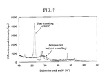
- the foregoing will be specifically explained based upon a measurement result of X-ray diffraction concerning a ZnInS thin film alone in Example 7 below.
- a transparent conductive film formed, for example, of ITO (In 2 O 3 -SnO 2 ), tin oxide (SnO 2 ), or ZnO:Al (produced by adding aluminum (Al) to zinc oxide (ZnO)) can be used.
- ITO In 2 O 3 -SnO 2
- SnO 2 tin oxide
- ZnO:Al produced by adding aluminum (Al) to zinc oxide (ZnO)
- vacuum vapor deposition, sputtering, etc. can be used as a method for forming the second electrode 105.
- the thickness of the second electrode 105 is preferably in the range of 50 nm to 200 nm.
- All of the first electrode 102, the p-type layer 103, the n-type layer 104 and the second electrode 105, shown in FIG. 1 are preferably formed by sputtering.
- a sputtering target a compound (alloy) target containing constituent elements in a state of a compound is used.
- an intended compound may be produced by simultaneous film formation (co-sputtering) with a plurality of metal targets containing constituent elements.
- the above-mentioned other members are not particularly limited and may be suitably selected according to the intended purpose, and examples thereof include a gas barrier layer, a protective layer and a buffer layer.
- Examples of materials usable for the gas barrier layer include inorganic materials such as silicon nitride and silicon oxide.
- the thin-film solar battery of the present invention is capable of securing a favorable balance between high throughput and generation of carriers in an n-type semiconductor layer to realize high energy efficiency, and the thin-film solar battery can be suitably used as any type of thin-film solar battery, e.g., an amorphous silicon solar battery, a solar battery using a compound semiconductor film, an organic thin-film solar battery or a dye-sensitized solar battery, notably as a solar battery using a compound semiconductor film.
- any type of thin-film solar battery e.g., an amorphous silicon solar battery, a solar battery using a compound semiconductor film, an organic thin-film solar battery or a dye-sensitized solar battery, notably as a solar battery using a compound semiconductor film.
- Examples 1, 2, 3, 4, 5, 6, 7 and 8 each explain a photoelectric conversion property of a II-III(In)-VI(S) compound thin film used as the n-type layer 104.
- Cd (as a Group 12 element)
- Mn (as a Group 7 element)
- Sr (as a Group 2 element)
- Zn (as a Group 12 element)
- Example 5 a mixture of Zn (as a Group 12 element) and Sr (as a Group 2 element) was used.
- Example 6 a mixture of In and Ga (as Group 13 elements) was used.
- Examples 7 and 8 a mixture of S and O (as Group 16 elements) and a mixture of S and Se (as Group 16 elements) were respectively used.
- Example 9 a mixture of S and Te (as Group 16 elements) was used.
- Mg (as a Group 2 element) and Zn (as a Group 12 element) were used.
- Ba (as a Group 2 element) and Zn (as a Group 12 element) were used.
- B and In were used.
- Al and In (as Group 13 elements) were used.
- Examples 14, 15 and 16 each explain a property of a ZnInS thin film alone, in which Zn (as a Group 12 element) is used.
- FIG. 2 is a cross-sectional view of a structure used for measurement of a photoelectric conversion property.
- the structure was formed by laying a CdInS thin film 202 and Al thin films (Al electrodes) 203 as counter electrodes over a glass substrate 201 as a support substrate.
- the Al electrodes were shaped like rectangles with an electrode distance 204 of 0.25 mm and an electrode width (electrode length L with respect to a widthwise direction in FIG. 2 ) of 5 mm.
- the CdInS thin film was formed by RF magnetron sputtering.
- the film formation atmosphere employed was an argon (Ar) gas atmosphere, and the pressure was set at 0.6 Pa.
- the film formation temperature was set at room temperature, and the film formation was performed without heating the substrate in a forced manner.
- the CdInS thin film had a thickness of 500 nm. After formed, the CdInS thin film was subjected to post-annealing (heat treatment after its formation) using an infrared heating apparatus.
- the annealing atmosphere employed was a nitrogen (N 2 ) gas atmosphere, the pressure was set at atmospheric pressure, and the length of time of the post-annealing was 1 hour.
- the temperature at which the post-annealing was performed (hereinafter referred to also as "post-annealing temperature") was set at 300°C.
- the Al thin films 203 were formed as counter electrodes. Heating vapor deposition with a resistance wire was employed to form the Al thin films 203, and they were formed at room temperature.
- the Al thin films 203 each had a thickness of 150 nm.
- each CdInS thin film 202 was irradiated with light having an intensity of 4,000 lux. While a voltage of 5 V was being applied between the Al counter electrodes 203, the current value was measured, and the resistance value was calculated.
- the resistance value of the thin film having been subjected to the as-deposition (without post-annealing) changed from 9x10 7 ⁇ (before the light irradiation) to 8x10 6 ⁇ (after the light irradiation).
- the resistance value of the thin film having been subjected to the post-annealing at 300°C changed from 5x10 7 ⁇ (before the light irradiation) to 3x10 6 ⁇ (after the light irradiation). In both these cases, the resistance value decreased because of generation of a photoelectric current caused by the light irradiation.
- a CdInS thin film exhibits a photoelectric conversion property even in the case of as-deposition (without annealing) or low-temperature annealing at approximately 300°C and is therefore a material useful for forming a solar battery at a low process temperature.
- a photoelectric conversion property of an MnInS thin film alone, serving as a II-III(In)-VI(S) compound thin film (with inclusion of a manganese element as a Group 7 element) used as the n-type layer 104 of the thin-film solar battery in FIG. 1 is now explained.
- a structure used for measurement of a photoelectric conversion property is shown in the cross-sectional view of FIG. 2 , as is the structure of Example 1. Specifically, the structure was formed by laying an MnInS thin film 202 and Al thin films (Al electrodes) 203 as counter electrodes over a glass substrate 201 as a support substrate.
- the Al electrodes were shaped like rectangles with an electrode distance 204 of 0.25 mm and an electrode width (electrode length L with respect to a widthwise direction in FIG. 2 ) of 5 mm.
- the MnInS thin film was formed by RF magnetron sputtering.
- the film formation atmosphere employed was an argon (Ar) gas atmosphere, and the pressure was set at 0.6 Pa.
- the film formation temperature was set at room temperature, and the film formation was performed without heating the substrate in a forced manner.
- the MnInS thin film had a thickness of 500 nm. After formed, the MnInS thin film was subjected to post-annealing (heat treatment after its formation) using an infrared heating apparatus.
- the annealing atmosphere employed was a nitrogen (N 2 ) gas atmosphere, the pressure was set at atmospheric pressure, and the length of time of the post-annealing was 1 hour.
- the temperature at which the post-annealing was performed was set at 300°C.
- the Al thin films 203 were formed as counter electrodes. Heating vapor deposition with a resistance wire was employed to form the Al thin films 203, and they were formed at room temperature.
- the Al thin films 203 each had a thickness of 150 nm.
- each MnInS thin film 202 was irradiated with light having an intensity of 4,000 lux. While a voltage of 5 V was being applied between the Al counter electrodes 203, the current value was measured, and the resistance value was calculated.
- the resistance value of the thin film having been subjected to the as-deposition (without post-annealing) changed from 3x10 6 ⁇ (before the light irradiation) to 7x10 5 ⁇ (after the light irradiation).
- the resistance value of the thin film having been subjected to the post-annealing at 300°C changed from 1x10 6 ⁇ (before the light irradiation) to 7x10 5 ⁇ (after the light irradiation). In both these cases, the resistance value decreased because of generation of a photoelectric current caused by the light irradiation.
- a MnInS thin film exhibits a photoelectric conversion property even in the case of as-deposition (without annealing) or low-temperature annealing at approximately 300°C and is therefore a material useful for forming a solar battery at a low process temperature.
- a photoelectric conversion property of an SrInS thin film alone, serving as a II-III(In)-VI(S) compound thin film (with inclusion of a strontium element as a Group 2 element) used as the n-type layer 104 of the thin-film solar battery in FIG. 1 is now explained.
- a structure used for measurement of a photoelectric conversion property is shown in the cross-sectional view of FIG. 2 , as are the structures of Examples 1 and 2. Specifically, the structure was formed by laying an SrInS thin film 202 and Al thin films (Al electrodes) 203 as counter electrodes over a glass substrate 201 as a support substrate.
- the Al electrodes were shaped like rectangles with an electrode distance 204 of 0.25 mm and an electrode width (electrode length L with respect to a widthwise direction in FIG. 2 ) of 5 mm.
- the SrInS thin film was formed by RF magnetron sputtering.
- the film formation atmosphere employed was an argon (Ar) gas atmosphere, and the pressure was set at 0.6 Pa.
- the film formation temperature was set at room temperature, and the film formation was performed without heating the substrate in a forced manner.
- the SrInS thin film had a thickness of 500 nm. After formed, the SrInS thin film was subjected to post-annealing (heat treatment after its formation) using an infrared heating apparatus.
- the annealing atmosphere employed was a nitrogen (N 2 ) gas atmosphere, the pressure was set at atmospheric pressure, and the length of time of the post-annealing was 1 hour.
- the temperature at which the post-annealing was performed was set at 300°C.
- the Al thin films 203 were formed as counter electrodes. Heating vapor deposition with a resistance wire was employed to form the Al thin films 203, and they were formed at room temperature.
- the Al thin films 203 each had a thickness of 150 nm.
- each SrInS thin film 202 was irradiated with light having an intensity of 4,000 lux. While a voltage of 5 V was being applied between the Al counter electrodes 203, the current value was measured, and the resistance value was calculated.
- the resistance value of the thin film having been subjected to the as-deposition (without post-annealing) changed from 3x10 7 ⁇ (before the light irradiation) to 1x10 6 ⁇ (after the light irradiation).
- the resistance value of the thin film having been subjected to the post-annealing at 300°C changed from 7x10 6 ⁇ (before the light irradiation) to 8x10 5 ⁇ after the light irradiation). In both these cases, the resistance value decreased because of generation of a photoelectric current caused by the light irradiation.
- an SrInS thin film exhibits a photoelectric conversion property even in the case of as-deposition (without annealing) or low-temperature annealing at approximately 300°C and is therefore a material useful for forming a solar battery at a low process temperature.
- a photoelectric conversion property of a ZnInS thin film alone, serving as a II-III(In)-VI(S) compound thin film (with inclusion of a zinc element as a Group 12 element) used as the n-type layer 104 of the thin-film solar battery in FIG. 1 is now explained.
- a structure used for measurement of a photoelectric conversion property is shown in the cross-sectional view of FIG. 2 , as are the structures of Examples 1, 2 and 3. Specifically, the structure was formed by laying a ZnInS thin film 202 and Al thin films (Al electrodes) 203 as counter electrodes over a glass substrate 201 as a support substrate.
- the Al electrodes were shaped like rectangles with an electrode distance 204 of 0.25 mm and an electrode width (electrode length L with respect to a widthwise direction in FIG. 2 ) of 5 mm.
- the ZnInS thin film 202 was formed by RF magnetron sputtering.
- the film formation atmosphere employed was an argon (Ar) gas atmosphere, and the pressure was set at 0.6 Pa.
- the film formation temperature was set at room temperature, and the film formation was performed without heating the substrate in a forced manner.
- the ZnInS thin film 202 had a thickness of 500 nm. After formed, the ZnInS thin film was subjected to post-annealing (heat treatment after its formation) using an infrared heating apparatus.
- the annealing atmosphere employed was a nitrogen (N 2 ) gas atmosphere, the pressure was set at atmospheric pressure, and the length of time of the post-annealing was 1 hour.
- the temperature at which the post-annealing was performed was varied between 300°C and 500°C.
- the Al thin films 203 were formed as counter electrodes. Heating vapor deposition with a resistance wire was employed to form the Al thin films 203, and they were formed at room temperature.
- the Al thin films 203 each had a thickness of 150 nm.
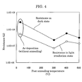
- FIG. 4 is a graph in which a photoelectric conversion property of the ZnInS thin film 202 is shown as a change in its resistance caused by light irradiation.
- a ZnInS thin film exhibits a photoelectric conversion property necessary for a constituent film of a thin-film solar battery.
- a ZnInS thin film exhibits a photoelectric conversion property even in the case of as-deposition (without annealing) or low-temperature annealing at approximately 300°C and is therefore a material useful for forming a solar battery at a low process temperature.
- a photoelectric conversion property of a ZnSrInS thin film alone, serving as a II-III(In)-VI(S) compound thin film (with inclusion of a zinc element as a Group 12 element and a strontium element as a Group 2 element) used as the n-type layer 104 of the thin-film solar battery in FIG. 1 is now explained.
- a structure used for measurement of a photoelectric conversion property is shown in the cross-sectional view of FIG. 2 , as are the structures of Examples 1, 2 and 3. Specifically, the structure was formed by laying a ZnSrInS thin film 202 and Al thin films (Al electrodes) 203 as counter electrodes over a glass substrate 201 as a support substrate.
- the Al electrodes were shaped like rectangles with an electrode distance 204 of 0.25 mm and an electrode width (electrode length L with respect to a widthwise direction in FIG. 2 ) of 5 mm.
- the ZnSrInS thin film 202 was formed by co-sputtering of ZnInS and SrS based upon RF magnetron sputtering.
- the film formation atmosphere employed was an argon (Ar) gas atmosphere, and the pressure was set at 0.6 Pa.
- the sputtering power for the ZnInS was set at 70 W and the sputtering power for the SrS was set at 20 W.
- the film formation temperature was set at room temperature, and the film formation was performed without heating the substrate in a forced manner.
- the ZnSrInS thin film had a thickness of 500 nm.
- the ZnSrInS thin film was subjected to post-annealing (heat treatment after its formation) using an infrared heating apparatus.
- the annealing atmosphere employed was a nitrogen (N 2 ) gas atmosphere, the pressure was set at atmospheric pressure, and the length of time of the post-annealing was 1 hour.
- the temperature at which the post-annealing was performed was set at 300°C.
- the Al thin films 203 were formed as counter electrodes. Heating vapor deposition with a resistance wire was employed to form the Al thin films 203, and they were formed at room temperature.
- the Al thin films 203 each had a thickness of 150 nm.
- each ZnSrInS thin film 202 was irradiated with light having an intensity of 4,000 lux. While a voltage of 5 V was being applied between the Al counter electrodes 203, the current value was measured, and the resistance value was calculated.
- the resistance value of the thin film having been subjected to the as-deposition (without post-annealing) changed from 4xl0 7 ⁇ (before the light irradiation) to 3x10 6 ⁇ (after the light irradiation).
- the resistance value of the thin film having been subjected to the post-annealing at 300°C changed from 1x10 7 ⁇ (before the light irradiation) to 6x10 5 ⁇ (after the light irradiation). In both these cases, the resistance value decreased because of generation of a photoelectric current caused by the light irradiation.
- a ZnSrInS thin film exhibits a photoelectric conversion property even in the case of as-deposition (without annealing) or low-temperature annealing at approximately 300°C and is therefore a material useful for forming a solar battery at a low process temperature.
- a photoelectric conversion property of a ZnInGaS thin film alone, serving as a II-III(In)-VI(S) compound thin film (with inclusion of an indium element and a gallium element as Group 13 elements) used as the n-type layer 104 of the thin-film solar battery in FIG. 1 is now explained.
- a structure used for measurement of a photoelectric conversion property is shown in the cross-sectional view of FIG. 2 , as are the structures of Examples 1, 2 and 3. Specifically, the structure was formed by laying a ZnInGaS thin film 202 and Al thin films (Al electrodes) 203 as counter electrodes over a glass substrate 201 as a support substrate.
- the Al electrodes were shaped like rectangles with an electrode distance 204 of 0.25 mm and an electrode width (electrode length L with respect to a widthwise direction in FIG. 2 ) of 5 mm.
- the ZnInGaS thin film 202 was formed by co-sputtering of ZnInS and GaS based upon RF magnetron sputtering.
- the sputtering power for the ZnInS was set at 70 W and the sputtering power for the GaS was set at 30 W.
- the film formation atmosphere employed was an argon (Ar) gas atmosphere, and the pressure was set at 0.6 Pa.
- the film formation temperature was set at room temperature, and the film formation was performed without heating the substrate in a forced manner.
- the ZnInGaS thin film had a thickness of 500 nm.
- the ZnInGaS thin film was subjected to post-annealing (heat treatment after its formation) using an infrared heating apparatus.
- the annealing atmosphere employed was a nitrogen (N 2 ) gas atmosphere, the pressure was set at atmospheric pressure, and the length of time of the post-annealing was 1 hour.
- the temperature at which the post-annealing was performed was set at 300°C.
- the Al thin films 203 were formed as counter electrodes. Heating vapor deposition with a resistance wire was employed to form the Al thin films 203, and they were formed at room temperature.
- the Al thin films 203 each had a thickness of 150 nm.
- each ZnInGaS thin film 202 was irradiated with light having an intensity of 4,000 lux. While a voltage of 5 V was being applied between the Al counter electrodes 203, the current value was measured, and the resistance value was calculated.
- the resistance value of the thin film having been subjected to the as-deposition (without post-annealing) changed from 9x10 6 ⁇ (before the light irradiation) to 3x10 5 ⁇ (after the light irradiation).
- the resistance value of the thin film having been subjected to the post-annealing at 300°C changed from 1x10 6 ⁇ (before the light irradiation) to 5x10 4 ⁇ (after the light irradiation). In both these cases, the resistance value decreased because of generation of a photoelectric current caused by the light irradiation.
- a ZnInGaS thin film exhibits a photoelectric conversion property even in the case of as-deposition (without annealing) or low-temperature annealing at approximately 300°C and is therefore a material useful for forming a solar battery at a low process temperature.
- a photoelectric conversion property of a ZnInSO thin film alone, serving as a II-III(In)-VI(S) compound thin film (with inclusion of a sulfur element and an oxygen element as Group 16 elements) used as the n-type layer 104 of the thin-film solar battery in FIG. 1 is now explained.
- a structure used for measurement of a photoelectric conversion property is shown in the cross-sectional view of FIG. 2 , as are the structures of Examples 1, 2 and 3. Specifically, the structure was formed by laying a ZnInSO thin film 202 and Al thin films (Al electrodes) 203 as counter electrodes over a glass substrate 201 as a support substrate.
- the Al electrodes were shaped like rectangles with an electrode distance 204 of 0.25 mm and an electrode width (electrode length L with respect to a widthwise direction in FIG. 2 ) of 5 mm.
- the ZnInSO thin film 202 was formed by reactive sputtering with oxygen based upon RF magnetron sputtering.
- the film formation atmosphere employed was an atmosphere of argon (Ar) gas and oxygen (O 2 ) gas, and the pressure was set at 0.6 Pa.
- the flow rate of the oxygen was set at 2.5% of the total flow rate of the gases.
- the film formation temperature was set at room temperature, and the film formation was performed without heating the substrate in a forced manner.
- the ZnInSO thin film had a thickness of 500 nm.
- the ZnInSO thin film was subjected to post-annealing (heat treatment after its formation) using an infrared heating apparatus.
- the annealing atmosphere employed was a nitrogen (N 2 ) gas atmosphere, the pressure was set at atmospheric pressure, and the length of time of the post-annealing was 1 hour.
- the temperature at which the post-annealing was performed was set at 300°C.
- the Al thin films 203 were formed as counter electrodes. Heating vapor deposition with a resistance wire was employed to form the Al thin films 203, and they were formed at room temperature.
- the Al thin films 203 each had a thickness of 150 nm.
- each ZnInSO thin film 202 was irradiated with light having an intensity of 4,000 lux. While a voltage of 5 V was being applied between the Al counter electrodes 203, the current value was measured, and the resistance value was calculated.
- the resistance value of the thin film having been subjected to the as-deposition (without post-annealing) changed from 9X10 7 ⁇ (before the light irradiation) to 3x10 6 ⁇ (after the light irradiation).
- the resistance value of the thin film having been subjected to the post-annealing at 300°C changed from 1x10 6 ⁇ (before the light irradiation) to 3x10 4 ⁇ (after the light irradiation). In both these cases, the resistance value decreased because of generation of a photoelectric current caused by the light irradiation.
- a ZnInSO thin film exhibits a photoelectric conversion property even in the case of as-deposition (without annealing) or low-temperature annealing at approximately 300°C and is therefore a material useful for forming a solar battery at a low process temperature.
- a photoelectric conversion property of a ZnInSSe thin film alone, serving as a II-III(In)-VI(S) compound thin film (with inclusion of a sulfur element and a selenium element as Group 16 elements) used as the n-type layer 104 of the thin-film solar battery in FIG. 1 is now explained.
- a structure used for measurement of a photoelectric conversion property is shown in the cross-sectional view of FIG. 2 , as are the structures of Examples 1, 2 and 3. Specifically, the structure was formed by laying a ZnInSSe thin film 202 and Al thin films (Al electrodes) 203 as counter electrodes over a glass substrate 201 as a support substrate.
- the Al electrodes were shaped like rectangles with an electrode distance 204 of 0.25 mm and an electrode width (electrode length L with respect to a widthwise direction in FIG. 2 ) of 5 mm.
- the ZnInSSe thin film 202 was formed by co-sputtering of ZnInS and Se based upon RF magnetron sputtering.
- the sputtering power for the ZnInS was set at 70 W and the sputtering power for the Se was set at 30 W.
- the film formation atmosphere employed was an argon (Ar) gas atmosphere, and the pressure was set at 0.6 Pa.
- the film formation temperature was set at room temperature, and the film formation was performed without heating the substrate in a forced manner.
- the ZnInSSe thin film had a thickness of 500 nm.
- the ZnInSSe thin film was subjected to post-annealing (heat treatment after its formation) using an infrared heating apparatus.
- the annealing atmosphere employed was a nitrogen (N 2 ) gas atmosphere, the pressure was set at atmospheric pressure, and the length of time of the post-annealing was 1 hour.
- the temperature at which the post-annealing was performed was set at 300°C.
- the Al thin films 203 were formed as counter electrodes. Heating vapor deposition with a resistance wire was employed to form the Al thin films 203, and they were formed at room temperature.
- the Al thin films 203 each had a thickness of 150 nm.
- each ZnInSSe thin film 202 was irradiated with light having an intensity of 4,000 lux. While a voltage of 5 V was being applied between the Al counter electrodes 203, the current value was measured, and the resistance value was calculated.
- the resistance value of the thin film having been subjected to the as-deposition (without post-annealing) changed from 2x10 6 ⁇ (before the light irradiation) to 3x10 5 ⁇ (after the light irradiation).
- the resistance value of the thin film having been subjected to the post-annealing at 300°C changed from 1x10 6 ⁇ (before the light irradiation) to 1x10 4 ⁇ (after the light irradiation). In both these cases, the resistance value decreased because of generation of a photoelectric current caused by the light irradiation.
- a ZnInSSe thin film exhibits a photoelectric conversion property even in the case of as-deposition (without annealing) or low-temperature annealing at approximately 300°C and is therefore a material useful for forming a solar battery at a low process temperature.
- a photoelectric conversion property of a ZnInSTe thin film alone, serving as a II-III(In)-VI(S) compound thin film (with inclusion of a sulfur element and a tellurium element as Group 16 elements) used as the n-type layer 104 of the thin-film solar battery in FIG. 1 is now explained.
- a structure used for measurement of a photoelectric conversion property is shown in the cross-sectional view of FIG. 2 , as are the structures of Examples 1, 2 and 3. Specifically, the structure was formed by laying a ZnInSTe thin film 202 and Al thin films (Al electrodes) 203 as counter electrodes over a glass substrate 201 as a support substrate.
- the Al electrodes were shaped like rectangles with an electrode distance 204 of 0.25 mm and an electrode width (electrode length L with respect to a widthwise direction in FIG. 2 ) of 5 mm.
- the ZnInSTe thin film 202 was formed by co-sputtering of ZnInS and Te based upon RF magnetron sputtering.
- the sputtering power for the ZnInS was set at 70 W and the sputtering power for the Te was set at 10 W.
- the film formation atmosphere employed was an argon (Ar) gas atmosphere, and the pressure was set at 0.6 Pa.
- the film formation temperature was set at room temperature, and the film formation was performed without heating the substrate in a forced manner.
- the ZnInSTe thin film had a thickness of 500 nm.
- the ZnInSTe thin film was subjected to post-annealing (heat treatment after its formation) using an infrared heating apparatus.
- the annealing atmosphere employed was a nitrogen (N 2 ) gas atmosphere, the pressure was set at atmospheric pressure, and the length of time of the post-annealing was 1 hour.
- the temperature at which the post-annealing was performed was set at 300°C.
- the Al thin films 203 were formed as counter electrodes. Heating vapor deposition with a resistance wire was employed to form the Al thin films 203, and they were formed at room temperature.
- the Al thin films 203 each had a thickness of 150 nm.
- each ZnInSTe thin film 202 was irradiated with light having an intensity of 4,000 lux. While a voltage of 5 V was being applied between the Al counter electrodes 203, the current value was measured, and the resistance value was calculated.
- the resistance value of the thin film having been subjected to the as-deposition (without post-annealing) changed from 3x10 7 ⁇ before the light irradiation) to 1x10 6 ⁇ (after the light irradiation).
- the resistance value of the thin film having been subjected to the post-annealing at 300°C changed from 4x10 6 ⁇ (before the light irradiation) to 8x10 4 ⁇ (after the light irradiation). In both these cases, the resistance value decreased because of generation of a photoelectric current caused by the light irradiation.
- a ZnInSTe thin film exhibits a photoelectric conversion property even in the case of as-deposition (without annealing) or low-temperature annealing at approximately 300°C and is therefore a material useful for forming a solar battery at a low process temperature.
- a photoelectric conversion property of a ZnMgInS thin film alone, serving as a II-III(In)-VI(S) compound thin film (with inclusion of a magnesium element as a Group 2 element and a zinc element as a Group 12 element) used as the n-type layer 104 of the thin-film solar battery in FIG. 1 is now explained.
- a structure used for measurement of a photoelectric conversion property is shown in the cross-sectional view of FIG. 2 , as are the structures of Examples 1, 2 and 3. Specifically, the structure was formed by laying a ZnMgInS thin film 202 and Al thin films (Al electrodes) 203 as counter electrodes over a glass substrate 201 as a support substrate.
- the Al electrodes were shaped like rectangles with an electrode distance 204 of 0.25 mm and an electrode width (electrode length L with respect to a widthwise direction in FIG. 2 ) of 5 mm.
- the ZnMgInS thin film 202 was formed by sputtering with the use of a ZnInS target with magnesium tips placed thereon, based upon RF magnetron sputtering.
- the sputtering power was set at 70 W.
- the film formation atmosphere employed was an argon (Ar) gas atmosphere, and the pressure was set at 0.6 Pa.
- the film formation temperature was set at room temperature, and the film formation was performed without heating the substrate in a forced manner.
- the ZnMgInS thin film had a thickness of 500 nm.
- the ZnMgInS thin film was subjected to post-annealing (heat treatment after its formation) using an infrared heating apparatus.
- the annealing atmosphere employed was a nitrogen (N 2 ) gas atmosphere, the pressure was set at atmospheric pressure, and the length of time of the post-annealing was 1 hour.
- the temperature at which the post-annealing was performed was set at 300°C.
- the Al thin films 203 were formed as counter electrodes. Heating vapor deposition with a resistance wire was employed to form the Al thin films 203, and they were formed at room temperature.
- the Al thin films 203 each had a thickness of 150 nm.
- each ZnMgInS thin film 202 was irradiated with light having an intensity of 4,000 lux. While a voltage of 5 V was being applied between the Al counter electrodes 203, the current value was measured, and the resistance value was calculated.
- the resistance value of the thin film having been subjected to the as-deposition (without post-annealing) changed from 5x10 7 ⁇ (before the light irradiation) to 5x10 6 ⁇ (after the light irradiation).
- the resistance value of the thin film having been subjected to the post-annealing at 300°C changed from 8x10 6 ⁇ (before the light irradiation) to 1x10 5 ⁇ (after the light irradiation). In both these cases, the resistance value decreased because of generation of a photoelectric current caused by the light irradiation.
- a ZnMgInS thin film exhibits a photoelectric conversion property even in the case of as-deposition (without annealing) or low-temperature annealing at approximately 300°C and is therefore a material useful for forming a solar battery at a low process temperature.
- a photoelectric conversion property of a ZnBaInS thin film alone, serving as a II-III(In)-VI(S) compound thin film (with inclusion of a barium element as a Group 2 element and a zinc element as a Group 12 element) used as the n-type layer 104 of the thin-film solar battery in FIG. 1 is now explained.
- a structure used for measurement of a photoelectric conversion property is shown in the cross-sectional view of FIG. 2 , as are the structures of Examples 1, 2 and 3. Specifically, the structure was formed by laying a ZnBaInS thin film 202 and Al thin films (Al electrodes) 203 as counter electrodes over a glass substrate 201 as a support substrate.
- the Al electrodes were shaped like rectangles with an electrode distance 204 of 0.25 mm and an electrode width (electrode length L with respect to a widthwise direction in FIG. 2 ) of 5 mm.
- the ZnBaInS thin film 202 was formed by co-sputtering of ZnInS and BaInS based upon RF magnetron sputtering.
- the sputtering power for the ZnInS was set at 70 W and the sputtering power for the BaInS was set at 15 W.
- the film formation atmosphere employed was an argon (Ar) gas atmosphere, and the pressure was set at 0.6 Pa.
- the film formation temperature was set at room temperature, and the film formation was performed without heating the substrate in a forced manner.
- the ZnBaInS thin film had a thickness of 500 nm.
- the ZnBaInS thin film was subjected to post-annealing (heat treatment after its formation) using an infrared heating apparatus.
- the annealing atmosphere employed was a nitrogen (N 2 ) gas atmosphere, the pressure was set at atmospheric pressure, and the length of time of the post-annealing was 1 hour.
- the temperature at which the post-annealing was performed was set at 300°C.
- the Al thin films 203 were formed as counter electrodes. Heating vapor deposition with a resistance wire was employed to form the Al thin films 203, and they were formed at room temperature.
- the Al thin films 203 each had a thickness of 150 nm.
- each ZnBaInS thin film 202 was irradiated with light having an intensity of 4,000 lux. While a voltage of 5 V was being applied between the Al counter electrodes 203, the current value was measured, and the resistance value was calculated.
- the resistance value of the thin film having been subjected to the as-deposition (without post-annealing) changed from 7xl0 7 ⁇ (before the light irradiation) to 3x10 6 ⁇ (after the light irradiation).
- the resistance value of the thin film having been subjected to the post-annealing at 300°C changed from 1x10 6 ⁇ (before the light irradiation) to 8x10 4 ⁇ (after the light irradiation). In both these cases, the resistance value decreased because of generation of a photoelectric current caused by the light irradiation.
- a ZnBaInS thin film exhibits a photoelectric conversion property even in the case of as-deposition (without annealing) or low-temperature annealing at approximately 300°C and is therefore a material useful for forming a solar battery at a low process temperature.
- a photoelectric conversion property of a ZnBInS thin film alone, serving as a II-III(In)-VI(S) compound thin film (with inclusion of a boron element and an indium element as Group 13 elements) used as the n-type layer 104 of the thin film solar battery in FIG. 1 is now explained.
- a structure used for measurement of a photoelectric conversion property is shown in the cross-sectional view of FIG. 2 , as are the structures of Examples 1, 2 and 3. Specifically, the structure was formed by laying a ZnBInS thin film 202 and Al thin films (Al electrodes) 203 as counter electrodes over a glass substrate 201 as a support substrate.
- the Al electrodes were shaped like rectangles with an electrode distance 204 of 0.25 mm and an electrode width (electrode length L with respect to a widthwise direction in FIG. 2 ) of 5 mm.
- the ZnBInS thin film 202 was formed by sputtering with the use of a ZnInS target with boron tips placed thereon, based upon RF magnetron sputtering.
- the sputtering power was set at 70 W.
- the film formation atmosphere employed was an argon (Ar) gas atmosphere, and the pressure was set at 0.6 Pa.
- the film formation temperature was set at room temperature, and the film formation was performed without heating the substrate in a forced manner.
- the ZnBInS thin film had a thickness of 500 nm.
- the ZnBInS thin film was subjected to post-annealing (heat treatment after its formation) using an infrared heating apparatus.
- the annealing atmosphere employed was a nitrogen (N 2 ) gas atmosphere, the pressure was set at atmospheric pressure, and the length of time of the post-annealing was 1 hour.
- the temperature at which the post-annealing was performed was set at 300°C.
- the Al thin films 203 were formed as counter electrodes. Heating vapor deposition with a resistance wire was employed to form the Al thin films 203, and they were formed at room temperature.
- the Al thin films 203 each had a thickness of 150 nm.
- each ZnBInS thin film 202 was irradiated with light having an intensity of 4,000 lux. While a voltage of 5 V was being applied between the Al counter electrodes 203, the current value was measured, and the resistance value was calculated.
- the resistance value of the thin film having been subjected to the as-deposition (without post-annealing) changed from 3x10 7 ⁇ (before the light irradiation) to 6x10 6 ⁇ (after the light irradiation).
- the resistance value of the thin film having been subjected to the post-annealing at 300°C changed from 2x10 6 ⁇ (before the light irradiation) to 9x10 4 ⁇ (after the light irradiation). In both these cases, the resistance value decreased because of generation of a photoelectric current caused by the light irradiation.
- a ZnBInS thin film exhibits a photoelectric conversion property even in the case of as-deposition (without annealing) or low-temperature annealing at approximately 300°C and is therefore a material useful for forming a solar battery at a low process temperature.
- a photoelectric conversion property of a ZnAlInS thin film alone, serving as a II-III(In)-VI(S) compound thin film (with inclusion of an aluminum element and an indium element as Group 13 elements) used as the n-type layer 104 of the thin-film solar battery in FIG. 1 is now explained.
- a structure used for measurement of a photoelectric conversion property is shown in the cross-sectional view of FIG. 2 , as are the structures of Examples 1, 2 and 3. Specifically, the structure was formed by laying a ZnAlInS thin film 202 and Al thin films (Al electrodes) 203 as counter electrodes over a glass substrate 201 as a support substrate.
- the Al electrodes were shaped like rectangles with an electrode distance 204 of 0.25 mm and an electrode width (electrode length L with respect to a widthwise direction in FIG. 2 ) of 5 mm.
- the ZnAlInS thin film 202 was formed by sputtering with the use of a ZnInS target with aluminum tips placed thereon, based upon RF magnetron sputtering.
- the sputtering power was set at 70 W.
- the film formation atmosphere employed was an argon (Ar) gas atmosphere, and the pressure was set at 0.6 Pa.
- the film formation temperature was set at room temperature, and the film formation was performed without heating the substrate in a forced manner.
- the ZnAlInS thin film had a thickness of 500 nm.
- the ZnAlInS thin film was subjected to post-annealing (heat treatment after its formation) using an infrared heating apparatus.
- the annealing atmosphere employed was a nitrogen (N 2 ) gas atmosphere, the pressure was set at atmospheric pressure, and the length of time of the post-annealing was 1 hour.
- the temperature at which the post-annealing was performed was set at 300°C.
- the Al thin films 203 were formed as counter electrodes. Heating vapor deposition with a resistance wire was employed to form the Al thin films 203, and they were formed at room temperature.
- the Al thin films 203 each had a thickness of 150 nm.
- each ZnAlInS thin film 202 was irradiated with light having an intensity of 4,000 lux. While a voltage of 5 V was being applied between the Al counter electrodes 203, the current value was measured, and the resistance value was calculated.
- the resistance value of the thin film having been subjected to the as-deposition (without post-annealing) changed from 8x10 6 ⁇ (before the light irradiation) to 9x10 5 ⁇ (after the light irradiation).
- the resistance value of the thin film having been subjected to the post-annealing at 300°C changed from 2x10 6 ⁇ (before the light irradiation) to 7x10 4 ⁇ (after the light irradiation). In both these cases, the resistance value decreased because of generation of a photoelectric current caused by the light irradiation.
- a ZnAlInS thin film exhibits a photoelectric conversion property even in the case of as-deposition (without annealing) or low-temperature annealing at approximately 300°C and is therefore a material useful for forming a solar battery at a low process temperature.
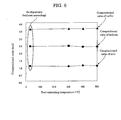
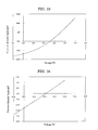
- the mobility of the ZnInS thin film 202 is shown in FIG. 5 .
- the mobility of the as-deposited ZnInS thin was 14 cm 2 /Vs, and the mobility decreased as the post-annealing temperature increased. It was presumed that the decrease in the mobility upon the high-temperature annealing was caused by the occurrence of a defect related to the heat treatment.
- a photoelectric conversion layer of a solar battery there is no clear reference value for the mobility of the photoelectric conversion layer; nevertheless, it is desirable that the mobility thereof be made as high as possible so as not to hinder the movement of a photoelectric current (generated by light irradiation) to an electrode.
- a ZnInS thin film exhibits high mobility even in the case of as-deposition (without annealing) or a low-temperature heat treatment such as annealing at 300°C, and is therefore a material useful for forming a thin-film solar battery at a low process temperature.
- compositional ratio between constituent elements of a ZnInS thin film 202 used as the n-type layer 104 of the thin-film solar battery in FIG. 1 is now explained.
- the compositional ratio was measured by energy dispersive X-ray spectrometry (EDS).
- EDS energy dispersive X-ray spectrometry
- a sample of a ZnInS thin film used for the measurement was produced in the same manner as in Example 4.
- the layer structure shown in FIG. 3 was employed, in which a ZnInS thin film 202 was laid on a glass substrate 201, and the thickness of the ZnInS thin film was 500 nm.
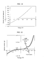
- the result of the measurement of the ZnInS thin film by the EDS is shown in FIG. 6 .
- the compositional ratio of Zn to In to S, which were the constituent elements, is shown as a molar ratio.
- the ZnInS thin film was a stable compound which hardly experienced compositional variation related to the heat treatment.
- the crystalline state of a ZnInS thin film, used as the n-type layer 104 of the thin-film solar battery in FIG. 1 is now explained based upon a measurement result of X-ray diffraction.
- a sample of a ZnInS thin film used for the measurement was produced in the same manner as in Example 4.
- the layer structure shown in FIG. 3 was employed, in which a ZnInS thin film 202 was laid on a glass substrate 201, and the thickness of the ZnInS thin film was 500 nm.
- the measurement of X-ray diffraction was carried out at a voltage of 45 kV and an electric current of 40 mA, with a Cu-k ⁇ ray.
- X-ray diffraction profiles in relation to the ZnInS thin film are shown in FIG. 7 .
- the diffraction profile of the ZnInS thin film in the case of as-deposition (without annealing) broadened with no clear diffraction peak observed. It was found that the as-deposited thin film was an aggregate of very small crystal grains. Meanwhile, regarding the diffraction profile of the ZnInS thin film having been subjected to post-annealing (500°C), an intense diffraction peak was observed in the vicinity of 22°.
- the thin film having been subjected to the annealing had larger crystal grains than the thin film in the as-deposited state and was an oriented film with the crystal grains being oriented in a certain crystal direction.
- changes in angle and half width according to the post-annealing temperature are shown in FIG. 8 .
- the angle and the half width regarding an X-ray diffraction peak of the ZnInS thin film changed in phases according to the post-annealing temperature.
- the half width of a diffraction peak could be defined as greater than 3° as a threshold value showing the state of a ZnInS thin film produced by as-deposition or a low-temperature process involving post-annealing at 300°C.
- each of the II-III(In)-VI(S) compound thin films wherein Cd (as a Group 12 element), Mn (as a Group 7 element), Sr (as a Group 2 element) and Zn (as a Group 12 element) were respectively used in Examples of 1, 2, 3 and 4, and Zn (as a Group 12 element), Sr (as a Group 2 element), a combination of In and Ga (as Group 13 elements), a combination of S and O (as Group 16 elements) and a combination of S and Se (as Group 16 elements) were respectively used in Examples 5, 6, 7 and 8, yielded a photoelectric conversion property even in a production method involving as-deposition or a low-temperature process such as post-annealing at 300°C, subsequent to the film formation by sputtering at room temperature without heating of the substrate, and therefore had a property suitable for a photoelectric conversion layer of a solar battery.
- Examples 4, 14, 15 and 16 demonstrated that each of the II-III(In)-VI(S) compound thin films, wherein Zn (as a Group 12 element) was used, yielded a photoelectric conversion property, was of n-type as a conduction type and had high mobility (7 cm 2 /Vs) even in a production method involving as-deposition or a low-temperature process such as post-annealing at 300°C, subsequent to the film formation by sputtering at room temperature, and thus demonstrated that each of the thin films had properties suitable for a photoelectric conversion layer of a solar battery. Further, it was demonstrated that these properties could be obtained even in an amorphous state with the half width of an X-ray diffraction peak being greater than 3°.
- any of the II-III(In)-VI(S) compound thin films produced by as-deposition or low-temperature annealing at approximately 300°C, subsequent to the film formation at room temperature it was possible to shorten the time spent in increasing and lowering the temperature in the production process. Therefore, high throughput in the production of thin-film solar batteries can be achieved, which leads to reduction in production costs. Also, since the film formation is performed at room temperature by means of sputtering, a low-temperature process in which heating of the support substrate 101 was not required could be employed, thereby making it possible to utilize a low-cost plastic substrate as the support substrate 101. Further, it was found that there were many merits including the fact that the occurrence of crack formation and film peeling, caused by residual stress relaxation related to high-temperature annealing, could be reduced.
- a thin-film solar battery having the structure shown in FIG. 1 AgInTe was used for the p-type layer 103, ZnInS was used for a II-III(In)-VI(S) compound thin film as the n-type layer 104, molybdenum (Mo) was used for the first electrode 102, and ZnO:Al was used for the second electrode 105, with all these members deposited by sputtering.
- a glass substrate was used as the support substrate 101.
- Mo used for the first electrode 102 was deposited by DC magnetron sputtering. With the input power being set at 3 kW, the Mo was deposited in an argon (Ar) gas atmosphere. The layer thickness thereof was 200 nm.
- AgInTe used for the p-type layer 103 was deposited by RF magnetron sputtering.
- ZnInS used for the n-type layer 104 was deposited by RF magnetron sputtering.
- post-annealing was carried out. Using an infrared heating furnace, the post-annealing was carried out in a nitrogen atmosphere. The post-annealing temperature was set at 300°C, and the pressure was set at atmospheric pressure.
- ZnO:Al used for the second electrode 105 was deposited by DC magnetron sputtering.
- the input power being set at 1 kW
- the ZnO:Al was deposited in an argon (Ar) gas atmosphere.
- the layer thickness thereof was 150 nm.
- the deposition temperature was set at room temperature (without carrying out heating of the substrate in a forced manner).
- a current-voltage (I-V) characteristic as an electricity-generating property of the thin-film solar battery of Example 17 is shown in FIG. 9 .
- a solar simulator with an artificial sunlight source with an intensity of 100 mW/cm 2 and an AM (air mass) of 1.5 was used. While a bias voltage in the range of ⁇ 0.2 V to + 0.6 V was being applied to the side of the Mo electrode as the first electrode 102, measurement was carried out with the side of the ZnO:Al electrode as the second electrode 105 being earthed.
- An I-V curve in a dark state and an I-V curve in a light irradiation state are shown in FIG. 9 .
- Such an electricity-generating property was obtained that the I-V curve shifted toward the negative electric current side by light irradiation and an electric current flowed even when there was no bias (0V).
- the thin-film solar battery wherein ZnInS was used for the n-type layer 104, AgInTe was used for the p-type layer 103, and all of the n-type layer 104, the p-type layer 103, the Mo first electrode 102 and the ZnO:Al second electrode (transparent conductive film) 105 were produced by sputtering yielded an electricity-generating property.
- the production of these members only by sputtering made it possible to produce uniform thin films with large areas and to achieve reduction in production costs by the use of a single film forming apparatus.
- Example 17 a thin-film solar battery containing a tellurium compound used for the p-type layer 103 was described.
- Example 18 a thin-film solar battery containing CuInS, which is a sulfide material as a material other than any tellurium compound, used for the p-type layer 103 is described.
- CuInS was used for the p-type layer 103
- ZnInS was used for a II-III(In)-VI(S) compound thin film as the n-type layer 104
- molybdenum (Mo) was used for the first electrode 102
- ZnO:Al was used for the second electrode 105, with all these members deposited by sputtering.
- a glass substrate was used as the support substrate 101.
- Mo used for the first electrode 102 was deposited by DC magnetron sputtering. With the input power being set at 3 kW, the Mo was deposited in an argon (Ar) gas atmosphere. The layer thickness thereof was 200 nm.
- CuInS used for the p-type layer 103 was deposited by RF magnetron sputtering.
- ZnInS used for the n-type layer 104 was deposited by co-sputtering in which two sputtering targets, i.e., ZnS and InS, were used.
- RF magnetron sputtering was employed, with the input powers for the ZnS target and the InS target being set at 0.2 kW and 0.1 kW respectively.
- the ZnInS was deposited in an argon (Ar) gas atmosphere.
- the layer thickness of the ZnInS was 500 nm. All these members were deposited at room temperature (without carrying out heating of the substrate in a forced manner).
- post-annealing was carried out. Using an infrared heating furnace, the post-annealing was carried out in a nitrogen atmosphere. The post-annealing temperature was set at 300°C, and the pressure was set at atmospheric pressure.
- ZnO:Al used for the second electrode 105 was deposited by DC magnetron sputtering.
- the input power being set at 1 kW
- the ZnO:Al was deposited in an argon (Ar) gas atmosphere.
- the layer thickness thereof was 150 nm.
- the deposition temperature was set at room temperature (without carrying out heating of the substrate in a forced manner).
- a current-voltage (I-V) characteristic as an electricity-generating property of the thin-film solar battery of Example 18 is shown in FIG. 10 .
- I-V characteristic For evaluation of the I-V characteristic, a solar simulator with an artificial sunlight source with an intensity of 100 mW/cm 2 and an AM (air mass) of 1.5 was used. While a bias voltage in the range of ⁇ 0.1 V to + 0.5 V was being applied to the side of the Mo electrode as the first electrode 102, measurement was carried out with the side of the ZnO:Al electrode as the second electrode 105 being earthed.
- An I-V curve in a dark state and an I-V curve in a light irradiation state are shown in FIG. 10 . Such an electricity-generating property was obtained that the I-V curve shifted toward the negative electric current side by light irradiation and an electric current flowed even when there was no bias (0V).
- the production of the members only by sputtering made it possible to produce uniform thin films with large areas and to achieve reduction in production costs by the use of a single film forming apparatus.
- Example 17 post-annealing was carried out at 300°C after the deposition of the ZnInS.
- Example 19 differences in electricity-generating property, related to the post-annealing temperature, are explained.
- a thin-film solar battery having the structure shown in FIG. 1 AgInTe was used for the p-type layer 103, ZnInS was used for a II-III(In)-VI(S) compound thin film as the n-type layer 104, molybdenum (Mo) was used for the first electrode 102, and ZnO:Al was used for the second electrode 105, with all these members deposited by sputtering.
- a glass substrate was used as the support substrate 101.
- Mo used for the first electrode 102 was deposited by DC magnetron sputtering. With the input power being set at 3 kW, the Mo was deposited in an argon (Ar) gas atmosphere. The layer thickness thereof was 200 nm.
- AgInTe used for the p-type layer 103 was deposited by RF magnetron sputtering.
- ZnInS used for the n-type layer 104 was formed by co-sputtering in which two sputtering targets, i.e., ZnS and InS, were used.
- RF magnetron sputtering was employed, with the input powers for the ZnS target and the InS target being set at 0.2 kW and 0.1 kW respectively.
- the ZnInS was deposited in an argon (Ar) gas atmosphere.
- the layer thickness of the ZnInS was 500 nm. All these members were deposited at room temperature (without carrying out heating of the substrate in a forced manner).
- post-annealing was carried out. Using an infrared heating furnace, the post-annealing was carried out in a nitrogen atmosphere. The pressure was set at atmospheric pressure. The post-annealing temperatures were set at 100°C, 200°C, 300°C and 400°C.
- a (non-annealed) sample not subjected to annealing in other words a sample simply formed at room temperature, was prepared.
- ZnO:Al used for the second electrode 105 was deposited by DC magnetron sputtering.
- the input power being set at 1 kW
- the ZnO:Al was deposited in an argon (Ar) gas atmosphere.
- the layer thickness thereof was 150 nm.
- the deposition temperature was set at room temperature (without carrying out heating of the substrate in a forced manner).
- FIG. 11 A current-voltage (I-V) characteristic as an electricity-generating property of the thin-film solar battery of Example 19 is shown in FIG. 11 .
- a solar simulator with an artificial sunlight source with an intensity of 100 mW/cm 2 and an AM (air mass) of 1.5 was used. While a bias voltage in the range of ⁇ 0.1 V to + 0.4 V was being applied to the side of the Mo electrode as the first electrode 102, measurement was carried out with the side of the ZnO:Al electrode as the second electrode 105 being earthed.
- the horizontal axis denotes applied voltage
- the vertical axis denotes current density
- only an I-V curve in a light irradiation state is shown.
- I-V curves respectively related to a non-annealed state and post-annealing temperatures of 100°C, 200°C, 300°C and 400°C are shown in FIG. 11 .
- Indices that show properties of a solar battery include open-circuit voltage (Voc) and short-circuit current (Isc). The greater the open-circuit voltage (Voc) and the short-circuit current (Isc) are, the better properties the solar battery has.
- the x-axis intercept corresponds to the short-circuit current (Isc)
- the y-axis intercept corresponds to the open-circuit voltage (Voc).
- both the short-circuit current (Isc) and the open-circuit voltage (Voc) increased as the post-annealing temperature rose.
- both the short-circuit current (Isc) and the open-circuit voltage (Voc) decreased. This result shows that the most suitable post-annealing temperature is 300°C or so.
- ⁇ favorable electricity-generating property was obtained by carrying out low-temperature heat treatment at a post-annealing temperature of 300°C.
- the structure was such that ZnO:Al used for the first electrode 102, ZnInS used for a II-III(In)-VI(S) compound thin film as the n-type layer, AgInTe used for the p-type layer, and molybdenum (Mo) used for the second electrode 105 were deposited in this order over the support substrate 101.
- a glass substrate was used as the support substrate 101.
- ZnO:Al used for the first electrode 102 was deposited by DC magnetron sputtering.
- the input power being set at 1 kW, the ZnO:Al was deposited in an argon (Ar) gas atmosphere.
- the layer thickness thereof was 150 nm.
- ZnInS used for the n-type layer 104 was deposited by RF magnetron sputtering.
- AgInTe used for the p-type layer was formed by RF magnetron sputtering.
- post-annealing was carried out. Using an infrared heating furnace, the post-annealing was carried out in a nitrogen atmosphere. The post-annealing temperature was set at 250°C, and the pressure was set at atmospheric pressure.
- Mo used for the second electrode 105 was deposited by DC magnetron sputtering. With the input power being set at 3 kW, the Mo was deposited in an argon (Ar) gas atmosphere. The layer thickness thereof was 200 nm. The deposition temperature was set at room temperature (without carrying out heating of the substrate in a forced manner).
- a current-voltage (I-V) characteristic as an electricity-generating property of the thin-film solar battery of Example 20 is shown in FIG. 12 .
- I-V characteristic For evaluation of the I-V characteristic, a solar simulator with an artificial sunlight source with an intensity of 100 mW/cm 2 and an AM (air mass) of 1.5 was used. While a bias voltage in the range of ⁇ 0.1 V to + 0.6 V was being applied to the side of the Mo electrode as the second electrode 105, measurement was carried out with the side of the ZnO:Al electrode as the first electrode 102 being earthed.
- An I-V curve in a dark state and an I-V curve in a light irradiation state are shown in FIG. 12 . Such an electricity-generating property was obtained that the I-V curve shifted toward the negative electric current side by light irradiation and an electric current flowed even when there was no bias (0V).
- FIG. 9 shows a result in relation to Example 17, yielded by earlier depositing AgInTe for the p-type layer, and then depositing ZnInS for the n-type layer.
- FIG. 12 shows a result in relation to Example 20, yielded by earlier depositing ZnInS for the n-type layer, and then depositing AgInTe for the p-type layer.
- a thin-film solar battery having the structure shown in FIG. 1 AgInTe was used for the p-type layer 103, ZnSrInS was used for a II-III(In)-VI(S) compound thin film as the n-type layer 104, molybdenum (Mo) was used for the first electrode 102, and ZnO:Al was used for the second electrode 105, with all these members deposited by sputtering.
- a glass substrate was used as the support substrate 101.
- Mo used for the first electrode 102 was deposited by DC magnetron sputtering. With the input energy being set at 3 kW, the Mo was deposited in an argon (Ar) gas atmosphere. The layer thickness thereof was 200 nm.
- AgInTe used for the p-type layer 103 was deposited by RF magnetron sputtering.
- ZnSrInS used for the n-type layer 104 was deposited by co-sputtering of ZnInS and SrS based upon RF magnetron sputtering.
- the ZnSrInS was deposited in an argon (Ar) gas atmosphere, and the pressure was set at 0.6 Pa.
- the sputtering powers for the ZnInS and the SrS were set at 70 W and 20 W respectively.
- the deposition temperature was set at room temperature (without carrying out heating of the substrate in a forced manner).
- the layer thickness of the ZnSrInS was 500 nm.
- post-annealing was carried out. Using an infrared heating furnace, the post-annealing was carried out in a nitrogen atmosphere. The post-annealing temperature was set at 300°C, and the pressure was set at atmospheric pressure.
- ZnO:Al used for the second electrode 105 was deposited by DC magnetron sputtering.
- the input power being set at 1 kW
- the ZnO:Al was deposited in an argon (Ar) gas atmosphere.
- the layer thickness thereof was 150 nm.
- the deposition temperature was set at room temperature (without carrying out heating of the substrate in a forced manner).
- a current-voltage (I-V) characteristic as an electricity-generating property of the thin-film solar battery of Example 21 is shown in FIG. 13 .
- I-V characteristic For evaluation of the I-V characteristic, a solar simulator with an artificial sunlight source with an intensity of 100 mW/cm 2 and an AM (air mass) of 1.5 was used. While a bias voltage in the range of ⁇ 0.2 V to + 0.6 V was being applied to the side of the Mo electrode as the first electrode 102, measurement was carried out with the side of the ZnO:Al electrode as the second electrode 105 being earthed.
- An I-V curve in a light irradiation state is shown in FIG. 13 . Such an electricity-generating property was obtained that the I-V curve shifted toward the negative electric current side by light irradiation and an electric current flowed even when there was no bias (0V).
- the thin-film solar battery wherein ZnSrInS was used for the n-type layer 104, AgInTe was used for the p-type layer 103, and all of the n-type layer 104, the p-type layer 103, the Mo first electrode 102 and the ZnO:Al second electrode (transparent conductive film) 105 were produced by sputtering yielded an electricity-generating property.
- the production of these members only by sputtering made it possible to produce uniform thin films with large areas and to achieve reduction in production costs by the use of a single film forming apparatus.
- CuInS was used for the p-type layer 103
- ZnInSO was used for a II-III(In)-VI(S) compound thin film as the n-type layer 104
- molybdenum (Mo) was used for the first electrode 102
- ZnO:Al was used for the second electrode 105, with all these members deposited by sputtering.
- a glass substrate was used as the support substrate 101.
- Mo used for the first electrode 102 was deposited by DC magnetron sputtering. With the input power being set at 3 kW, the Mo was deposited in an argon (Ar) gas atmosphere. The layer thickness thereof was 200 nm.
- CuInS used for the p-type layer 103 was deposited by RF magnetron sputtering.
- ZnInSO used for the n-type layer 104 was deposited by reactive sputtering with oxygen based upon RF magnetron sputtering.
- the ZnInSO was deposited in an atmosphere of argon (Ar) gas and oxygen (O 2 ) gas, and the pressure was set at 0.6 Pa.
- the flow rate of the oxygen was set at 2.5% of the total flow rate of the gases.
- the deposition temperature was set at room temperature (without carrying out heating of the substrate in a forced manner).
- the thickness of the ZnInSO thin film was 500 nm.
- post-annealing was carried out. Using an infrared heating furnace, the post-annealing was carried out in a nitrogen atmosphere. The post-annealing temperature was set at 300°C, and the pressure was set at atmospheric pressure.
- ZnO:Al used for the second electrode 105 was deposited by DC magnetron sputtering.
- the input power being set at 1 kW
- the ZnO:Al was deposited in an argon (Ar) gas atmosphere.
- the layer thickness thereof was 150 nm.
- the deposition temperature was set at room temperature (without carrying out heating of the substrate in a forced manner).
- a current-voltage (I-V) characteristic as an electricity-generating property of the thin-film solar battery of Example 22 is shown in FIG. 14 .
- I-V characteristic For evaluation of the I-V characteristic, a solar simulator with an artificial sunlight source with an intensity of 100 mW/cm 2 and an AM (air mass) of 1.5 was used. While a bias voltage in the range of ⁇ 0.1 V to + 0.5 V was being applied to the side of the Mo electrode as the first electrode 102, measurement was carried out with the side of the ZnO:Al electrode as the second electrode 105 being earthed.
- An I-V curve in a light irradiation state is shown in FIG. 14 . Such an electricity-generating property was obtained that the I-V curve shifted toward the negative electric current side by light irradiation and an electric current flowed even when there was no bias (0V).
- the thin-film solar battery wherein ZnInSO was used for the n-type layer 104, CuInS was used for the p-type layer 103, and all of the n-type layer 104, the p-type layer 103, the Mo first electrode 102 and the ZnO:Al second electrode (transparent conductive film) 105 were produced by sputtering yielded an electricity-generating property.
- the production of these members only by sputtering made it possible to produce uniform thin films with large areas and to achieve reduction in production costs by the use of a single film forming apparatus.
- CuInS was used for the p-type layer 103
- ZnInGaS was used for a II-III(In)-VI(S) compound thin film as the n-type layer 104
- molybdenum (Mo) was used for the first electrode 102
- ZnO:Al was used for the second electrode 105, with all these members deposited by sputtering.
- a glass substrate was used as the support substrate 101.
- Mo used for the first electrode 102 was deposited by DC magnetron sputtering. With the input power being set at 3 kW, the Mo was deposited in an argon (Ar) gas atmosphere. The layer thickness thereof was 200 nm.
- CuInS used for the p-type layer 103 was deposited by RF magnetron sputtering.
- ZnInGaS used for the n-type layer 104 was deposited by co-sputtering of ZnInS and ZnGaS based upon RF magnetron sputtering.
- the ZnInGaS was deposited in an argon (Ar) gas atmosphere, and the pressure was set at 0.6 Pa.
- the sputtering powers for the ZnInS and the ZnGaS were set at 70 W and 30 W respectively.
- the deposition temperature was set at room temperature (without carrying out heating of the substrate in a forced manner).
- the layer thickness of the ZnInGaS was 500 nm.
- post-annealing was carried out. Using an infrared heating furnace, the post-annealing was carried out in a nitrogen atmosphere. The post-annealing temperature was set at 300°C, and the pressure was set at atmospheric pressure.
- ZnO:A1 used for the second electode 105 was deposited by DC magnetron sputtering.
- the input power being set at 1 kW
- the ZnO:Al was deposited in an argon (Ar) gas atmosphere.
- the layer thickness thereof was 150 nm.
- the deposition temperature was set at room temperature (without carrying out heating of the substrate in a forced manner).
- a current-voltage (I-V) characteristic as an electricity-generating property of the thin-film solar battery of Example 23 is shown in FIG. 15 .
- I-V characteristic For evaluation of the I-V characteristic, a solar simulator with an artificial sunlight source with an intensity of 100 mW/cm 2 and an AM (air mass) of 1.5 was used. While a bias voltage in the range of ⁇ 0.1 V to + 0.5 V was being applied to the side of the Mo electrode as the first electrode 102, measurement was carried out with the side of the ZnO:Al electrode as the second electrode 105 being earthed.
- An I-V curve in a light irradiation state is shown in FIG. 15 . Such an electricity-generating property was obtained that the I-V curve shifted toward the negative electric current side by light irradiation and an electric current flowed even when there was no bias (0V).
- the thin-film solar battery wherein ZnInGaS was used for the n-type layer 104, CuInS was used for the p-type layer 103, and all of the n-type layer 104, the p-type layer 103, the Mo first electrode 102 and the ZnO:Al second electrode (transparent conductive film) 105 were produced by sputtering yielded an electricity-generating property.
- the production of these members only by sputtering made it possible to produce uniform thin films with large areas and to achieve reduction in production costs by the use of a single film forming apparatus.
- a thin-film solar battery having the structure shown in FIG. 1 AgInTe was used for the p-type layer 103, ZnMnInS was used for a II-III(In)-VI(S) compound thin film as the n-type layer 104, molybdenum (Mo) was used for the first electrode 102, and ZnO:Al was used for the second electrode 105, with all these members deposited by sputtering.
- a glass substrate was used as the support substrate 101.
- Mo used for the first electrode 102 was deposited by DC magnetron sputtering. With the input power being set at 3 kW, the Mo was deposited in an argon (Ar) gas atmosphere. The layer thickness thereof was 200 nm.
- AgInTe used for the p-type layer 103 was deposited by RF magnetron sputtering.
- ZnMnInS used for the n-type layer 104 was deposited by co-sputtering of ZnInS and MnInS based upon RF magnetron sputtering.
- the ZnMnInS was deposited in an argon (Ar) gas atmosphere, and the pressure was set at 0.6 Pa.
- the sputtering powers for the ZnInS and the MnInS were set at 70 W and 30 W respectively.
- the deposition temperature was set at room temperature (without carrying out heating of the substrate in a forced manner).
- the layer thickness of the ZnMnInS was 500 nm.
- post-annealing was carried out. Using an infrared heating furnace, the post-annealing was carried out in a nitrogen atmosphere. The post-annealing temperature was set at 300°C, and the pressure was set at atmospheric pressure.
- ZnO:Al used for the second electrode 105 was deposited by DC magnetron sputtering.
- the input power being set at 1 kW
- the ZnO:Al was deposited in an argon (Ar) gas atmosphere.
- the layer thickness thereof was 150 nm.
- the deposition temperature was set at room temperature (without carrying out heating of the substrate in a forced manner).
- a current-voltage (I-V) characteristic as an electricity-generating property of the thin-film solar battery of Example 24 is shown in FIG. 16 .
- I-V characteristic For evaluation of the I-V characteristic, a solar simulator with an artificial sunlight source with an intensity of 100 mW/cm 2 and an AM (air mass) of 1.5 was used. While a bias voltage in the range of ⁇ 0.1 V to + 0.5 V was being applied to the side of the Mo electrode as the first electrode 102, measurement was carried out with the side of the ZnO:Al electrode as the second electrode 105 being earthed.
- An I-V curve in a light irradiation state is shown in FIG. 16 . Such an electricity-generating property was obtained that the I-V curve shifted toward the negative electric current side by light irradiation and an electric current flowed even when there was no bias (0V).
- the thin-film solar battery wherein ZnMnInS was used for the n-type layer 104, AgInTe was used for the p-type layer 103, and all of the n-type layer 104, the p-type layer 103, the Mo first electrode 102 and the ZnO:Al second electrode (transparent conductive film) 105 were produced by sputtering yielded an electricity-generating property.
- the production of these members only by sputtering made it possible to produce uniform thin films with large areas and to achieve reduction in production costs by the use of a single film forming apparatus.
- a thin-film solar battery having the structure shown in FIG. 1 AgInTe was used for the p-type layer 103, ZnSrInGaS was used for a II-III(In)-VI(S) compound thin film as the n-type layer 104, molybdenum (Mo) was used for the first electrode 102, and ZnO:Al was used for the second electrode 105, with all these members deposited by sputtering.
- a glass substrate was used as the support substrate 101.
- Mo used for the first electrode 102 was deposited by DC magnetron sputtering. With the input power being set at 3 kW, the Mo was deposited in an argon (Ar) gas atmosphere. The layer thickness thereof was 200 nm.
- AgInTe used for the p-type layer 103 was deposited by RF magnetron sputtering.
- ZnSrInGaS used for the n-type layer 104 was deposited by co-sputtering of ZnGaS and SrInS based upon RF magnetron sputtering.
- the ZnSrInGaS was deposited in an argon (Ar) gas atmosphere, and the pressure was set at 0.6 Pa.
- the sputtering powers for the ZnGaS and the SrInS were set at 40 W and 70 W respectively.
- the deposition temperature was set at room temperature (without carrying out heating of the substrate in a forced manner).
- the layer thickness of the ZnSrInGaS was 500 nm.
- post-annealing was carried out. Using an infrared heating furnace, the post-annealing was carried out in a nitrogen atmosphere. The post-annealing temperature was set at 300°C, and the pressure was set at atmospheric pressure.
- ZnO:Al used for the second electrode 105 was deposited by DC magnetron sputtering.
- the input power being set at 1 kW
- the ZnO:Al was deposited in an argon (Ar) gas atmosphere.
- the layer thickness thereof was 150 nm.
- the deposition temperature was set at room temperature (without carrying out heating of the substrate in a forced manner).
- a current-voltage (I-V) characteristic as an electricity-generating property of the thin-film solar battery of Example 25 is shown in FIG. 17 .
- I-V characteristic For evaluation of the I-V characteristic, a solar simulator with an artificial sunlight source with an intensity of 100 mW/cm 2 and an AM (air mass) of 1.5 was used. While a bias voltage in the range of ⁇ 0.1 V to + 0.5 V was being applied to the side of the Mo electrode as the first electrode 102, measurement was carried out with the side of the ZnO:Al electrode as the second electrode 105 being earthed.
- An I-V curve in a light irradiation state is shown in FIG. 17 . Such an electricity-generating property was obtained that the I-V curve shifted toward the negative electric current side by light irradiation and an electric current flowed even when there was no bias (0V).
- the thin-film solar battery wherein ZnSrInGaS was used for the n-type layer 104, AgInTe was used for the p-type layer 103, and all of the n-type layer 104, the p-type layer 103, the Mo first electrode 102 and the ZnO:Al second electrode (transparent conductive film) 105 were produced by sputtering yielded an electricity-generating property.
- the production of these members only by sputtering made it possible to produce uniform thin films with large areas and to achieve reduction in production costs by the use of a single film forming apparatus.
- CuInS was used for the p-type layer 103
- CaInS was used for a II-III(In)-VI(S) compound thin film as the n-type layer 104
- molybdenum (Mo) was used for the first electrode 102
- ZnO:Al was used for the second electrode 105, with all these members deposited by sputtering.
- a glass substrate was used as the support substrate 101.
- Mo used for the first electrode 102 was deposited by DC magnetron sputtering. With the input power being set at 3 kW, the Mo was deposited in an argon (Ar) gas atmosphere. The layer thickness thereof was 200 nm.
- CuInS used for the p-type layer 103 was deposited by RF magnetron sputtering.
- CaInS used for the n-type layer 104 was deposited by RF magnetron sputtering.
- the sputtering power was set at 70 W.
- the deposition temperature was set at room temperature (without carrying out heating of the substrate in a forced manner).
- the layer thickness of the CaInS was 500 nm.
- post-annealing was carried out. Using an infrared heating furnace, the post-annealing was carried out in a nitrogen atmosphere. The post-annealing temperature was set at 300°C, and the pressure was set at atmospheric pressure.
- ZnO:Al used for the second electrode 105 was deposited by DC magnetron sputtering.
- the input power being set at 1 kW
- the ZnO:Al was deposited in an argon (Ar) gas atmosphere.
- the layer thickness thereof was 150 nm.
- the deposition temperature was set at room temperature (without carrying out heating of the substrate in a forced manner).
- a current-voltage (I-V) characteristic as an electricity-generating property of the thin-film solar battery of Example 26 is shown in FIG. 18 .
- I-V characteristic For evaluation of the I-V characteristic, a solar simulator with an artificial sunlight source with an intensity of 100 mW/cm 2 and an AM (air mass) of 1.5 was used. While a bias voltage in the range of ⁇ 0.1 V to + 0.5 V was being applied to the side of the Mo electrode as the first electrode 102, measurement was carried out with the side of the ZnO:Al electrode as the second electrode 105 being earthed.
- An I-V curve in a light irradiation state is shown in FIG. 18 . Such an electricity-generating property was obtained that the I-V curve shifted toward the negative electric current side by light irradiation and an electric current flowed even when there was no bias (0V).
- the thin-film solar battery wherein CaInS was used for the n-type layer 104, CuInS was used for the p-type layer 103, and all of the n-type layer 104, the p-type layer 103, the Mo first electrode 102 and the ZnO:Al second electrode (transparent conductive film) 105 were produced by sputtering yielded an electricity-generating property.
- the production of these members only by sputtering made it possible to produce uniform thin films with large areas and to achieve reduction in production costs by the use of a single film forming apparatus.
- Cu2S was used for the p-type layer 103
- ZnInS was used for a II-III(In)-VI(S) compound thin film as the n-type layer 104
- molybdenum (Mo) was used for the first electrode 102
- ZnO:Al was used for the second electrode 105, with all these members deposited by sputtering.
- a glass substrate was used as the support substrate 101.
- Mo used for the first electrode 102 was deposited by DC magnetron sputtering. With the input power being set at 3 kW, the Mo was deposited in an argon (Ar) gas atmosphere. The layer thickness thereof was 200 nm.
- Cu2S used for the p-type layer 103 was deposited by RF magnetron sputtering.
- the Cu2S was deposited in an argon (Ar) gas atmosphere.
- the layer thickness thereof was 500 nm. Note that when a photoelectric conversion property of the Cu2S thin film alone was examined using a method similar to that in Examples 1 to 8, a photoelectric current was not generated by light irradiation.
- ZnInS used for the n-type layer 104 was deposited by RF magnetron sputtering.
- the ZnInS was deposited in an argon (Ar) gas atmosphere, and the pressure was set at 0.6 Pa.
- the sputtering power was set at 70 W.
- the deposition temperature was set at room temperature (without carrying out heating of the substrate in a forced manner).
- the layer thickness of the ZnInS was 500 nm.
- post-annealing was carried out. Using an infrared heating furnace, the post-annealing was carried out in a nitrogen atmosphere. The post-annealing temperature was set at 300°C, and the pressure was set at atmospheric pressure.
- ZnO:Al used for the second electrode 105 was deposited by DC magnetron sputtering.
- the input power being set at 1 kW
- the ZnO:Al was deposited in an argon (Ar) gas atmosphere.
- the layer thickness thereof was 150 nm.
- the deposition temperature was set at room temperature (without carrying out heating of the substrate in a forced manner).
- a current-voltage (I-V) characteristic as an electricity-generating property of the thin-film solar battery of Example 27 is shown in FIG. 19 .
- I-V characteristic For evaluation of the I-V characteristic, a solar simulator with an artificial sunlight source with an intensity of 100 mW/cm 2 and an AM (air mass) of 1.5 was used. While a bias voltage in the range of ⁇ 0.1 V to + 0.5 V was being applied to the side of the Mo electrode as the first electrode 102, measurement was carried out with the side of the ZnO:Al electrode as the second electrode 105 being earthed.
- An I-V curve in a light irradiation state is shown in FIG. 19 . Such an electricity-generating property was obtained that the I-V curve shifted toward the negative electric current side by light irradiation and an electric current flowed even when there was no bias (0V).
- the thin-film solar battery wherein ZnInS was used for the n-type layer 104, Cu2S was used for the p-type layer 103, and all of the n-type layer 104, the p-type layer 103, the Mo first electrode 102 and the ZnO:Al second electrode (transparent conductive film) 105 were produced by sputtering yielded an electricity-generating property.
- the production of these members only by sputtering made it possible to produce uniform thin films with large areas and to achieve reduction in production costs by the use of a single film forming apparatus.
- a thin-film solar battery having the structure shown in FIG. 1 AgInTe was used for the p-type layer 103, ZnO was used for the n-type layer 104, molybdenum (Mo) was used for the first electrode 102, and ITO was used for the second electrode 105, with all these members deposited by sputtering.
- a glass substrate was used as the support substrate 101.
- Mo used for the first electrode 102 was formed by DC magnetron sputtering. With the input power being set at 3 kW, the Mo was deposited in an argon (Ar) gas atmosphere. The layer thickness thereof was 200 nm.
- AgInTe used for the p-type layer 103 was deposited by RF magnetron sputtering.
- ZnO used for the n-type layer 104 was formed by RF magnetron sputtering.
- the ZnO was deposited in an argon (Ar) gas atmosphere.
- the layer thickness thereof was 150 nm. All these members were deposited at room temperature (without carrying out heating of the substrate in a forced manner).
- post-annealing was carried out. Using an infrared heating furnace, the post-annealing was carried out in a nitrogen atmosphere. The post-annealing temperature was set at 250°C, and the pressure was set at atmospheric pressure.
- ITO used for the second electrode 105 was deposited by DC magnetron sputtering.
- a sputtering target In 2 O 3 with 5 mol% of SnO 2 added thereto was used.
- the input power being set at 0.4 kW, the ITO was deposited in a mixed atmosphere of Argon (Ar) gas and oxygen (O 2 ) gas, in which the O 2 gas was added in an amount of 5% with respect to the Ar gas.
- the layer thickness thereof was 150 nm.
- the deposition temperature was set at room temperature (without carrying out heating of the substrate in a forced manner).
- a current-voltage (I-V) characteristic as an electricity-generating property of the thin-film solar battery of Comparative Example 1 is shown in FIG. 20 .
- a light source for evaluation of the I-V characteristic a halogen lamp with an illuminance of 4,000 lux was used. While a bias voltage in the range of ⁇ 0.5 V to + 0.5 V was being applied to the side of the Mo electrode as the first electrode 102, measurement was carried out with the side of the ITO electrode as the second electrode 105 being earthed.
- An I-V curve in a dark state and an I-V curve in a light irradiation state are shown in FIG. 20 . Change in the I-V curve caused by light irradiation was not observed, and the I-V curve was a curve passing through the point 0.
- a thin-film solar battery having the structure shown in FIG. 1 AgInTe was used for the p-type layer 103, a laminated film of ZnS/ZnO was used for the n-type layer 104, molybdenum (Mo) was used for the first electrode 102, and ITO was used for the second electrode 105, with all these members deposited by sputtering.
- a glass substrate was used as the support substrate 101.
- Mo used for the first electrode 102 was deposited by DC magnetron sputtering. With the input power being set at 3 kW, the Mo was deposited in an argon (Ar) gas atmosphere. The layer thickness thereof was 200 nm.
- AgInTe used for the p-type layer 103 was deposited by RF magnetron sputtering.
- a laminated film of ZnS/ZnO as the n-type layer 104 was formed by RF magnetron sputtering.
- post-annealing was carried out. Using an infrared heating furnace, the post-annealing was carried out in a nitrogen atmosphere. The post-annealing temperature was set at 300°C, and the pressure was set at atmospheric pressure.
- ITO as the second electrode 105 was deposited by DC magnetron sputtering.
- a sputtering target In 2 O 3 with 5 mol% of SnO 2 added thereto was used.
- the input power being set at 0.4 kW, the ITO was deposited in a mixed atmosphere of Argon (Ar) gas and oxygen (O 2 ) gas, in which the O 2 gas was added in an amount of 5% with respect to the Ar gas.
- the layer thickness thereof was 150 nm.
- the deposition temperature was set at room temperature (without carrying out heating of the substrate in a forced manner).
- a current-voltage (I-V) characteristic as an electricity-generating property of the thin-film solar battery of Comparative Example 2 is shown in FIG. 21 .
- a halogen lamp with an illuminance of 4,000 lux was used as a light source for evaluation of the I-V characteristic. While a bias voltage in the range of ⁇ 0.5 V to + 0.5 V was being applied to the side of the Mo electrode as the first electrode 102, measurement was carried out with the side of the ITO electrode as the second electrode 105 being earthed.
- An I-V curve in a dark state and an I-V curve in a light irradiation state are shown in FIG. 21 . Change in the I-V curve caused by light irradiation was not observed, and the I-V curve was a curve passing through the point 0.
- Mo used for the first electrode 102 was deposited by DC magnetron sputtering. With the input power being set at 3 kW, the Mo was deposited in an argon (Ar) gas atmosphere. The layer thickness thereof was 200 nm.
- AgInTe used for the p-type layer 103 was deposited by RF magnetron sputtering.
- InS used for the n-type layer 104 was deposited by RF magnetron sputtering.
- post-annealing was carried out. Using an infrared heating furnace, the post-annealing was carried out in a nitrogen atmosphere. The post-annealing temperature was set at 250°C, and the pressure was set at atmospheric pressure.
- ZnO:Al used for the second electrode 105 was deposited by DC magnetron sputtering.
- the input power being set at 1 kW
- the ZnO:Al was deposited in an Argon (Ar) gas atmosphere.
- the layer thickness thereof was 150 nm.
- the deposition temperature was set at room temperature (without carrying out heating of the substrate in a forced manner).
- a current-voltage (I-V) characteristic as an electricity-generating property of the thin-film solar battery of Comparative Example 3 is shown in FIG. 22 .
- I-V characteristic For evaluation of the I-V characteristic, a solar simulator with an artificial sunlight source with an intensity of 100 mW/cm 2 and an AM (air mass) of 1.5 was used. While a bias voltage in the range of ⁇ 0.1 V to + 0.5 V was being applied to the side of the Mo electrode as the first electrode 102, measurement was carried out with the side of the ZnO:Al electrode as the second electrode 105 being earthed.
- An I-V curve in a light irradiation state is shown in FIG. 22 .
- the photoelectric conversion layer 100 has a laminated layer structure which includes at least the p-type layer 103 and the n-type layer 104, and the n-type layer 104 is a II-III(In)-VI(S) compound thin film which contains at least indium (In), sulfur (S) and element(s) (denoted by the sign II) of at least one group selected from Groups 2, 7 and 12.
- This structure has made it possible to obtain a thin-film solar battery using a compound semiconductor film, which secures a favorable balance between high energy efficiency and high throughput.
- the crystalline state of the II-III(In)-VI(S) compound thin film as the n-type layer 104 is an amorphous state.
- the II-III(In)-VI(S) compound thin film as the n-type layer 104 yields a photoelectric conversion property and has high mobility even with a low-temperature process such as post-annealing at 300°C, and the thin film therefore exhibits a property suitable for a photoelectric conversion layer of a solar battery.
- the II-III(In)-VI(S) compound thin film had large crystal grains in the case of a high-temperature process such as post-annealing at 400°C to 500°C, whereas the II-III(In)-VI(S) compound thin film was in an amorphous state in the case of a low-temperature process such as post-annealing at 300°C.
- the II-III(In)-VI(S) compound thin film that is in an amorphous state due to a low-temperature process can be used as a favorable n-type photoelectric conversion layer.
- the low-temperature annealing enables a low-cost plastic substrate to be utilized as the support substrate, which leads to reduction in costs. Also, there are merits including the fact that the occurrence of crack formation and film peeling, caused by residual stress relaxation related to high-temperature annealing, can be reduced.
- the II-III(In)-VI(S) compound thin film as the n-type layer 104 is formed by sputtering.
- Sputtering is simpler than vacuum vapor deposition, a selenization method and a CBD method that are widely used for producing compound semiconductor films.
- the production of the thin film by sputtering has made it possible to achieve even higher throughput. Also, it has been found that since an apparatus for sputtering is simple and uniform thin films can be produced with large areas, reduction in production costs can be achieved.
Landscapes
- Photovoltaic Devices (AREA)
Applications Claiming Priority (3)
| Application Number | Priority Date | Filing Date | Title |
|---|---|---|---|
| JP2010061572 | 2010-03-17 | ||
| JP2010061570 | 2010-03-17 | ||
| JP2011053113A JP5673236B2 (ja) | 2010-03-17 | 2011-03-10 | 薄膜太陽電池及びその製造方法 |
Publications (2)
| Publication Number | Publication Date |
|---|---|
| EP2367208A2 true EP2367208A2 (fr) | 2011-09-21 |
| EP2367208A3 EP2367208A3 (fr) | 2015-03-04 |
Family
ID=44118354
Family Applications (1)
| Application Number | Title | Priority Date | Filing Date |
|---|---|---|---|
| EP11250317.2A Withdrawn EP2367208A3 (fr) | 2010-03-17 | 2011-03-16 | Batterie solaire à couche mince et son procédé de production |
Country Status (3)
| Country | Link |
|---|---|
| US (1) | US20110226337A1 (fr) |
| EP (1) | EP2367208A3 (fr) |
| JP (1) | JP5673236B2 (fr) |
Cited By (1)
| Publication number | Priority date | Publication date | Assignee | Title |
|---|---|---|---|---|
| WO2013189976A1 (fr) * | 2012-06-20 | 2013-12-27 | Saint-Gobain Glass France | Système multicouche pour cellules solaires à films minces |
Families Citing this family (6)
| Publication number | Priority date | Publication date | Assignee | Title |
|---|---|---|---|---|
| JP2013229487A (ja) * | 2012-04-26 | 2013-11-07 | Kyocera Corp | 光電変換装置の製造方法 |
| JP2014130858A (ja) * | 2012-12-28 | 2014-07-10 | Fujifilm Corp | 光電変換素子および光電変換素子のバッファ層の製造方法 |
| US20140261651A1 (en) * | 2013-03-15 | 2014-09-18 | Nanoco Technologies, Ltd. | PV Device with Graded Grain Size and S:Se Ratio |
| JP2014209586A (ja) * | 2013-03-27 | 2014-11-06 | 株式会社リコー | 薄膜太陽電池及びその製造方法 |
| JP2015029031A (ja) | 2013-07-02 | 2015-02-12 | 株式会社リコー | 配線基板、及び配線基板の製造方法 |
| CN114277375A (zh) * | 2021-12-15 | 2022-04-05 | 青岛迪恩特尚核新材料科技有限公司 | 一种MnIn2S4/TiO2纳米管束丛复合光阳极材料及其制备方法和应用 |
Citations (2)
| Publication number | Priority date | Publication date | Assignee | Title |
|---|---|---|---|---|
| JP2003008039A (ja) | 2001-06-26 | 2003-01-10 | Sharp Corp | 化合物太陽電池の製造方法 |
| WO2005064692A1 (fr) | 2003-12-05 | 2005-07-14 | Matsushita Electric Industrial Co., Ltd. | Couche semi-conductrice composite, cellule solaire, et procede permettant de produire ceux-ci |
Family Cites Families (9)
| Publication number | Priority date | Publication date | Assignee | Title |
|---|---|---|---|---|
| JPH01128477A (ja) * | 1987-11-12 | 1989-05-22 | Ricoh Co Ltd | アモルファスシリコン光センサー |
| DE3903699A1 (de) * | 1988-02-08 | 1989-08-17 | Ricoh Kk | Bildsensor |
| US5053844A (en) * | 1988-05-13 | 1991-10-01 | Ricoh Company, Ltd. | Amorphous silicon photosensor |
| US5108843A (en) * | 1988-11-30 | 1992-04-28 | Ricoh Company, Ltd. | Thin film semiconductor and process for producing the same |
| JP2776009B2 (ja) * | 1990-07-16 | 1998-07-16 | 松下電器産業株式会社 | 太陽電池とその製造方法 |
| US8129822B2 (en) * | 2006-10-09 | 2012-03-06 | Solexel, Inc. | Template for three-dimensional thin-film solar cell manufacturing and methods of use |
| JP2006332373A (ja) * | 2005-05-26 | 2006-12-07 | Matsushita Electric Ind Co Ltd | 酸化物薄膜太陽電池 |
| US20090230594A1 (en) * | 2008-03-12 | 2009-09-17 | Hiroshi Deguchi | Imprint method and mold |
| WO2010090740A1 (fr) * | 2009-02-04 | 2010-08-12 | Heliovolt Corporation | Procédé de fabrication d'un film d'oxyde conducteur transparent contenant de l'indium, cibles métalliques utilisées dans le procédé et dispositifs photovoltaïques utilisant lesdits films |
-
2011
- 2011-03-10 JP JP2011053113A patent/JP5673236B2/ja not_active Expired - Fee Related
- 2011-03-16 US US13/049,079 patent/US20110226337A1/en not_active Abandoned
- 2011-03-16 EP EP11250317.2A patent/EP2367208A3/fr not_active Withdrawn
Patent Citations (2)
| Publication number | Priority date | Publication date | Assignee | Title |
|---|---|---|---|---|
| JP2003008039A (ja) | 2001-06-26 | 2003-01-10 | Sharp Corp | 化合物太陽電池の製造方法 |
| WO2005064692A1 (fr) | 2003-12-05 | 2005-07-14 | Matsushita Electric Industrial Co., Ltd. | Couche semi-conductrice composite, cellule solaire, et procede permettant de produire ceux-ci |
Cited By (6)
| Publication number | Priority date | Publication date | Assignee | Title |
|---|---|---|---|---|
| WO2013189976A1 (fr) * | 2012-06-20 | 2013-12-27 | Saint-Gobain Glass France | Système multicouche pour cellules solaires à films minces |
| CN104885205A (zh) * | 2012-06-20 | 2015-09-02 | 法国圣戈班玻璃厂 | 薄层太阳能电池的层系统 |
| US20160233360A1 (en) * | 2012-06-20 | 2016-08-11 | Saint-Gobain Glass France | Layer system for thin-film solar cells |
| KR101671090B1 (ko) | 2012-06-20 | 2016-10-31 | 쌩-고벵 글래스 프랑스 | 박막 태양 전지를 위한 층 시스템 |
| CN104885205B (zh) * | 2012-06-20 | 2017-06-20 | 法国圣戈班玻璃厂 | 薄层太阳能电池的层系统 |
| US10134931B2 (en) | 2012-06-20 | 2018-11-20 | Bengbu Design & Research Institute For Glass Industry | Layer system for thin-film solar cells |
Also Published As
| Publication number | Publication date |
|---|---|
| JP5673236B2 (ja) | 2015-02-18 |
| JP2011216874A (ja) | 2011-10-27 |
| EP2367208A3 (fr) | 2015-03-04 |
| US20110226337A1 (en) | 2011-09-22 |
Similar Documents
| Publication | Publication Date | Title |
|---|---|---|
| Gong et al. | Enhancing photocurrent of Cu (In, Ga) Se2 solar cells with actively controlled Ga grading in the absorber layer | |
| US5141564A (en) | Mixed ternary heterojunction solar cell | |
| EP2367208A2 (fr) | Batterie solaire à couche mince et son procédé de production | |
| AU2011226881B2 (en) | Photovoltaic device and method for making | |
| Tolstova et al. | Polycrystalline Cu2O photovoltaic devices incorporating Zn (O, S) window layers | |
| US20140290739A1 (en) | Thin-film solar battery and method of making same | |
| EP2768030A2 (fr) | Cellule solaire et son procédé de fabrication | |
| Li et al. | Influence of the selenization condition on the properties of ambient-air processed CZTSSe thin films and device performance | |
| US20120180858A1 (en) | Method for making semiconducting film and photovoltaic device | |
| WO2012118771A2 (fr) | Dispositifs photovoltaïques à couches minces améliorés et procédés de fabrication | |
| US9786804B2 (en) | Thin-film solar cell and production method for thin-film solar cell | |
| US12148854B2 (en) | Method for producing a double graded CdSeTe thin film structure | |
| Alberts | A comparison of the material and device properties of homogeneous and compositional-graded Cu (In, Ga)(Se, S) 2 chalcopyrite thin films | |
| US20120080306A1 (en) | Photovoltaic device and method for making | |
| Altamura et al. | Influence of sodium-containing substrates on Kesterite CZTSSe thin films based solar cells | |
| KR101708282B1 (ko) | CZTSe계 박막을 이용한 태양전지 및 이의 제조 방법 | |
| KR102015985B1 (ko) | 태양전지용 cigs 박막의 제조방법 | |
| Cantas | Photovoltaic Performance Investigation of Superstrate Sb2Se3 Solar Cells with Non-toxic Zn (O, S) Buffer Layer via Magnetron Sputtering | |
| Romeo | CdTe and CuInGaSe2 thin-film solar cells | |
| LU504697B1 (en) | Thin film solar cell and corresponding production method | |
| Hartman et al. | Impact of H 2 S annealing on SnS device performance | |
| Subramanian | Characterization of cadmium zinc telluride solar cells by RF sputtering | |
| Wang | N-Type CdTe Thin Films for Photovoltaic Applications | |
| Chandrasekaran | Effect of heat treatments and reduced absorber layer thickness on Cu (In, Ga) Se2 thin film solar cells | |
| JP5842991B2 (ja) | 化合物半導体太陽電池 |
Legal Events
| Date | Code | Title | Description |
|---|---|---|---|
| PUAI | Public reference made under article 153(3) epc to a published international application that has entered the european phase |
Free format text: ORIGINAL CODE: 0009012 |
|
| 17P | Request for examination filed |
Effective date: 20110404 |
|
| AK | Designated contracting states |
Kind code of ref document: A2 Designated state(s): AL AT BE BG CH CY CZ DE DK EE ES FI FR GB GR HR HU IE IS IT LI LT LU LV MC MK MT NL NO PL PT RO RS SE SI SK SM TR |
|
| AX | Request for extension of the european patent |
Extension state: BA ME |
|
| PUAL | Search report despatched |
Free format text: ORIGINAL CODE: 0009013 |
|
| AK | Designated contracting states |
Kind code of ref document: A3 Designated state(s): AL AT BE BG CH CY CZ DE DK EE ES FI FR GB GR HR HU IE IS IT LI LT LU LV MC MK MT NL NO PL PT RO RS SE SI SK SM TR |
|
| AX | Request for extension of the european patent |
Extension state: BA ME |
|
| RIC1 | Information provided on ipc code assigned before grant |
Ipc: H01L 31/0336 20060101ALI20150123BHEP Ipc: H01L 31/032 20060101AFI20150123BHEP |
|
| 17Q | First examination report despatched |
Effective date: 20171114 |
|
| STAA | Information on the status of an ep patent application or granted ep patent |
Free format text: STATUS: THE APPLICATION IS DEEMED TO BE WITHDRAWN |
|
| 18D | Application deemed to be withdrawn |
Effective date: 20180125 |