EP2369733A2 - Agencement de commutation et procédé de production d'une tension alternative à partir d'une multitude de sources de tension ayant une tension continue de sortie variable dans le temps - Google Patents
Agencement de commutation et procédé de production d'une tension alternative à partir d'une multitude de sources de tension ayant une tension continue de sortie variable dans le temps Download PDFInfo
- Publication number
- EP2369733A2 EP2369733A2 EP11151095A EP11151095A EP2369733A2 EP 2369733 A2 EP2369733 A2 EP 2369733A2 EP 11151095 A EP11151095 A EP 11151095A EP 11151095 A EP11151095 A EP 11151095A EP 2369733 A2 EP2369733 A2 EP 2369733A2
- Authority
- EP
- European Patent Office
- Prior art keywords
- circuit
- voltage
- arrangement according
- converter
- positive
- Prior art date
- Legal status (The legal status is an assumption and is not a legal conclusion. Google has not performed a legal analysis and makes no representation as to the accuracy of the status listed.)
- Granted
Links
Images


Classifications
-
- H—ELECTRICITY
- H02—GENERATION; CONVERSION OR DISTRIBUTION OF ELECTRIC POWER
- H02M—APPARATUS FOR CONVERSION BETWEEN AC AND AC, BETWEEN AC AND DC, OR BETWEEN DC AND DC, AND FOR USE WITH MAINS OR SIMILAR POWER SUPPLY SYSTEMS; CONVERSION OF DC OR AC INPUT POWER INTO SURGE OUTPUT POWER; CONTROL OR REGULATION THEREOF
- H02M7/00—Conversion of AC power input into DC power output; Conversion of DC power input into AC power output
- H02M7/42—Conversion of DC power input into AC power output without possibility of reversal
- H02M7/44—Conversion of DC power input into AC power output without possibility of reversal by static converters
- H02M7/48—Conversion of DC power input into AC power output without possibility of reversal by static converters using discharge tubes with control electrode or semiconductor devices with control electrode
- H02M7/53—Conversion of DC power input into AC power output without possibility of reversal by static converters using discharge tubes with control electrode or semiconductor devices with control electrode using devices of a triode or transistor type requiring continuous application of a control signal
- H02M7/537—Conversion of DC power input into AC power output without possibility of reversal by static converters using discharge tubes with control electrode or semiconductor devices with control electrode using devices of a triode or transistor type requiring continuous application of a control signal using semiconductor devices only, e.g. single switched pulse inverters
-
- H—ELECTRICITY
- H02—GENERATION; CONVERSION OR DISTRIBUTION OF ELECTRIC POWER
- H02J—ELECTRIC POWER NETWORKS; CIRCUIT ARRANGEMENTS OR SYSTEMS FOR SUPPLYING OR DISTRIBUTING ELECTRIC POWER; SYSTEMS FOR STORING ELECTRIC ENERGY
- H02J7/00—Circuit arrangements for charging or discharging batteries or for supplying loads from batteries
- H02J7/34—Parallel operation in networks using both storage and other DC sources, e.g. providing buffering
- H02J7/35—Parallel operation in networks using both storage and other DC sources, e.g. providing buffering with light sensitive cells
-
- H—ELECTRICITY
- H02—GENERATION; CONVERSION OR DISTRIBUTION OF ELECTRIC POWER
- H02M—APPARATUS FOR CONVERSION BETWEEN AC AND AC, BETWEEN AC AND DC, OR BETWEEN DC AND DC, AND FOR USE WITH MAINS OR SIMILAR POWER SUPPLY SYSTEMS; CONVERSION OF DC OR AC INPUT POWER INTO SURGE OUTPUT POWER; CONTROL OR REGULATION THEREOF
- H02M7/00—Conversion of AC power input into DC power output; Conversion of DC power input into AC power output
- H02M7/42—Conversion of DC power input into AC power output without possibility of reversal
- H02M7/44—Conversion of DC power input into AC power output without possibility of reversal by static converters
- H02M7/48—Conversion of DC power input into AC power output without possibility of reversal by static converters using discharge tubes with control electrode or semiconductor devices with control electrode
-
- H—ELECTRICITY
- H02—GENERATION; CONVERSION OR DISTRIBUTION OF ELECTRIC POWER
- H02M—APPARATUS FOR CONVERSION BETWEEN AC AND AC, BETWEEN AC AND DC, OR BETWEEN DC AND DC, AND FOR USE WITH MAINS OR SIMILAR POWER SUPPLY SYSTEMS; CONVERSION OF DC OR AC INPUT POWER INTO SURGE OUTPUT POWER; CONTROL OR REGULATION THEREOF
- H02M1/00—Details of apparatus for conversion
- H02M1/0067—Converter structures employing plural converter units, other than for parallel operation of the units on a single load
- H02M1/007—Plural converter units in cascade
-
- H—ELECTRICITY
- H02—GENERATION; CONVERSION OR DISTRIBUTION OF ELECTRIC POWER
- H02M—APPARATUS FOR CONVERSION BETWEEN AC AND AC, BETWEEN AC AND DC, OR BETWEEN DC AND DC, AND FOR USE WITH MAINS OR SIMILAR POWER SUPPLY SYSTEMS; CONVERSION OF DC OR AC INPUT POWER INTO SURGE OUTPUT POWER; CONTROL OR REGULATION THEREOF
- H02M7/00—Conversion of AC power input into DC power output; Conversion of DC power input into AC power output
- H02M7/42—Conversion of DC power input into AC power output without possibility of reversal
- H02M7/44—Conversion of DC power input into AC power output without possibility of reversal by static converters
- H02M7/48—Conversion of DC power input into AC power output without possibility of reversal by static converters using discharge tubes with control electrode or semiconductor devices with control electrode
- H02M7/53—Conversion of DC power input into AC power output without possibility of reversal by static converters using discharge tubes with control electrode or semiconductor devices with control electrode using devices of a triode or transistor type requiring continuous application of a control signal
- H02M7/537—Conversion of DC power input into AC power output without possibility of reversal by static converters using discharge tubes with control electrode or semiconductor devices with control electrode using devices of a triode or transistor type requiring continuous application of a control signal using semiconductor devices only, e.g. single switched pulse inverters
- H02M7/5387—Conversion of DC power input into AC power output without possibility of reversal by static converters using discharge tubes with control electrode or semiconductor devices with control electrode using devices of a triode or transistor type requiring continuous application of a control signal using semiconductor devices only, e.g. single switched pulse inverters in a bridge configuration
-
- Y—GENERAL TAGGING OF NEW TECHNOLOGICAL DEVELOPMENTS; GENERAL TAGGING OF CROSS-SECTIONAL TECHNOLOGIES SPANNING OVER SEVERAL SECTIONS OF THE IPC; TECHNICAL SUBJECTS COVERED BY FORMER USPC CROSS-REFERENCE ART COLLECTIONS [XRACs] AND DIGESTS
- Y02—TECHNOLOGIES OR APPLICATIONS FOR MITIGATION OR ADAPTATION AGAINST CLIMATE CHANGE
- Y02E—REDUCTION OF GREENHOUSE GAS [GHG] EMISSIONS, RELATED TO ENERGY GENERATION, TRANSMISSION OR DISTRIBUTION
- Y02E10/00—Energy generation through renewable energy sources
- Y02E10/50—Photovoltaic [PV] energy
- Y02E10/56—Power conversion systems, e.g. maximum power point trackers
Definitions
- the invention relates to a circuit arrangement, as well as a method for the control thereof, for generating an AC voltage from a plurality of unregulated voltage sources with time-variable DC output voltage.
- unregulated power sources photovoltaic systems or parts of these systems are preferred.
- a photovoltaic system is to be understood here exclusively as the arrangement and electrical connection of a plurality of photovoltaic modules, subsystems are also subsumed here.
- Such photovoltaic modules are combined to photovoltaic systems and have a design-dependent and dependent on the sunlight and thus temporally slowly variable output DC voltage. These changes in the DC output voltage have time constants in the minute range or in longer time units.
- the DC output voltage must be converted by means of an inverter circuit in an AC voltage of constant frequency and voltage.
- An exemplary circuit arrangement for generating such an AC voltage is in the DE 10 2008 034 955 A1 described.
- a power converter arrangement which has a photovoltaic system with time-varying output voltage, a level converter and an inverter.
- the first and second capacitors of the level converter are charged independently of the input voltage with half the value of the nominal intermediate circuit voltage.
- a disadvantage of such a circuit arrangements is that in this case the photovoltaic system is loaded with a current fluctuating briefly in the frequency range of the control of the level converter.
- the individual photovoltaic modules should be loaded as linearly as possible, i. Their output current should be as constant as possible in time within time intervals, as they are typical for power semiconductor circuits, ie in the time domain less than one second, or in a frequency range above 1Hz.
- the input voltage to the inverter circuit should be as constant as possible, as well as the transmission from the photovoltaic system to the inverter circuit with the highest possible voltage should be done to keep line losses small.
- the entire circuit arrangement should work with a high degree of efficiency, in this case the number of components required being small and their dimensioning, especially that of coils and capacitors, also be as small as possible.
- the photovoltaic system or its photovoltaic modules should be operated in such a way that it operates at the point of the highest power output (MPP).
- MPP highest power output
- a suitable regulation, the so-called. MPP tracking is required.
- the invention has for its object to provide a circuit arrangement and an associated method for generating an AC voltage from a plurality of voltage sources, each with time-varying DC output voltage, the current load is uniformly these voltage sources and the transfer to the inverter circuit with minimal losses.
- the circuit arrangement according to the invention comprises one or a plurality of parallel-connected subcircuit arrangements for feeding at least one inverter circuit, which can be connected to at least one associated transformer.
- each subcircuit arrangement consists of an unregulated voltage source with a time-varying DC output voltage, a voltage doubler circuit and a voltage regulator circuit with associated control device.
- the input voltage is doubled by means of the voltage doubling circuit by the two power transistors of the half-bridge circuit being offset in time and each with the same period of half of the switching period.
- the unregulated voltage source is charged constantly, that is, their output current has no fluctuations in the short-term range, ie in the range of one second or faster, as is particularly preferred for photovoltaic or photovoltaic modules.
- the voltage doubling circuit each has a branch of positive and negative polarity, wherein at their inputs in each case a first and second inductance, formed from a first and second coil or only from the inductance of the respective supply line from the voltage source is provided. At this first and second inductance shoots a half-bridge circuit of two power transistors between the positive and the negative pointer. Subsequently, in each case a diode is provided in both branches, and thereafter a series connection of two first capacitors, which connects the two branches.
- the first variant has two separate sub-circuits, an up-converter and a down-converter.
- two variants are also advantageous.
- the respective boost converters are provided immediately after the associated voltage doubler circuits in order to raise their output voltages to the same potential.
- the respective down converter is then provided in the inverter circuit to lower the transmission voltage there to a suitable value of the intermediate circuit voltage.
- This variant has the advantage of providing a particularly high voltage for power transmission between the photovoltaic system and the inverter circuit and thus to keep the line losses as low as possible. Consequently Also, the dimensioning of the transmission cables and the associated costs can be reduced because of the lower value of the transmission current.
- the second variant with two separate subcircuits has the respective buck converter in direct connection with the associated voltage doubler circuit, while the upconverter is located in the inverter circuit.
- the transmission is carried out at a lower voltage compared to the first variant.
- this can be advantageous in order to adapt the overall system to safety guidelines and not have to implement exemplary special protection regulations for higher voltages.
- the voltage regulation circuit with two separate converter circuits offers a high degree of flexibility for adapting the subcircuit arrangement to the application-specific circumstances.
- the second variant of the voltage regulation circuit is basically constructed identically to the voltage doubling circuit and can thus be advantageously produced with identical power semiconductor modules.
- this voltage regulation circuit is controlled differently according to its task to the voltage doubling circuit and serves to adapt the output DC voltage of the different circuit elements to be switched in parallel to each other.
- the MPP tracking is also carried out by the control device of the voltage control circuit in addition to the described adaptation of the output voltage of the voltage doubling circuit to the DC link voltage of the inverter circuit.
- inverter circuit fundamentally different three-phase inverters are providable. It is particularly advantageous to arrange two three-phase inverters in parallel and offset by half a switching period to control. This results in a desired sinusoidal output sufficiently approximated voltage.
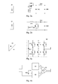
- Fig. 1 shows the basic principle of a first circuit arrangement according to the invention, as well as some of its components.
- Fig. 2 shows further components of a circuit arrangement according to the invention.
- Fig. 3 shows the basic principle of a further embodiments of the circuit arrangement according to the invention.
- Fig. 4 shows further components of a circuit arrangement according to the invention.
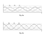
- Fig. 5 shows the simulation of the output current of a circuit arrangement according to the invention when using a method according to the invention.
- Fig. 1 shows schematically the basic principle of a first circuit arrangement according to the invention, as well as some of its components.
- an unregulated voltage source (12) here a photovoltaic system
- the known fluctuations in the DC output voltage as well as the output current due to the variation of solar radiation.
- MPP tracking For advantageous operation of such a photovoltaic system (12), it is necessary to regulate the output voltage and current in such a way that the output power is maximum. This is known as MPP tracking.
- MPP tracking MPP tracking.
- a voltage doubler circuit (20) adjoins the output of the photovoltaic system (12), which leads to an output current without short-term fluctuations.
- This voltage doubler circuit (20) shown in FIG Fig. 1b each having a branch of positive and negative polarity has an associated inductance (200, 202) in each branch.
- This inductance (200, 202) is formed here by the connecting lines between the photovoltaic system and the other components of the voltage doubling circuit. If the inductance (200, 202) of these leads should not be sufficient, it is additionally possible to provide coils with low inductance in comparison to the prior art.
- the voltage doubling circuit (20) here includes the connection line with the photovoltaic system (12). These connecting cables have a length dimension of the order of ten meters.
- a half-bridge circuit is provided between the positive and the negative branch.
- This half-bridge circuit in turn has a series connection of a first (210) and a second power transistor (212), possibly with antiparallel-connected freewheeling diodes.
- This half-bridge circuit is connected by means of a respective diode (220, 222) per branch to a series circuit (230, 232) of second capacitors (230, 232).
- a series circuit 230, 232
- the cathode is connected to the capacitor circuit.
- the cathode is connected to the half-bridge circuit and the anode to the capacitor circuit.
- both power transistors (210, 212) are switched on alternately for the same time interval in each case with a moderate switching frequency of preferably between 500 Hz and 2 kHz. There are also switching frequencies below 250Hz and up to 5kHz suitable but usually not necessary. Thus, there is always a current flow either through the first or through the second power transistor (210, 212) and thus the current load of the photovoltaic system (12) is kept constant. Constant means here there are no short-term fluctuations, especially in the order of magnitude of the drive frequency of the power transistor (210, 212).
- the voltage doubler circuit is followed by a voltage regulating circuit (30, 40), which can be designed differently depending on the conditions of use.
- the first variant has a combination of a down (34) and an up converter (32) whose order is basically arbitrary. Here, however, it is essential that the two converter circuits are not arranged directly adjacent, but that their connection line (300), according to Fig. 1c / d, the substantial distance between the photovoltaic system (12) and the inverter circuit (50) bridges.
- the voltage in the connection line (300) can be set below a defined threshold, illustratively below 600V or below 1000V. This can be the hassle for the Protection against contact dependent on national regulations against higher voltages substantially simplify.
- the second variant has as a voltage regulating circuit (40) to a subcircuit, which is identical to the voltage doubling circuit (20) is formed, but not how it is driven.
- the two switches are preferably for the same time intervals but with a suitable length and possibly overlap controlled to adjust the fluctuating input voltage to the desired constant output voltage.
- the MPP tracking of the photovoltaic system (12) is controlled by the voltage regulating circuit (30, 40), not by the voltage doubling circuit (20).
- the voltage doubler circuit (20) it is not necessary for the voltage doubler circuit (20) to have a control connection of its controller (250) to the voltage regulator circuit (30, 40) or the inverter circuit (50).
- the photovoltaic system (12), the voltage doubler circuit (20) and the respective voltage regulation circuit (30, 40) form a subcircuit arrangement, which is connected to an inverter circuit (50) to form a circuit arrangement according to the invention.
- Fig. 2 shows components of a circuit arrangement according to the invention, here the two converter circuits, which correspond to the prior art.
- the down converter (34) In its first branch, the one of positive polarity, has a power transistor (340). This is followed by a diode (342) connecting the first to the second branch and an inductor (344) in the first branch and a capacitor (346) connecting both branches. It may be sufficient in the above-mentioned application with a connection line following the down converter (34), said inductance (344) being determined by the inductance of the connection line (300, cf. Fig. 1d ) form, or provide a correspondingly small-sized coil.
- the boost converter (32), according to Fig. 2b Has in its first branch on an inductance (320), which also advantageously by a connecting line (300, see Fig. 1c ), possibly with an additional coil of low inductance, is formed. This is followed by a power transistor (322) connecting the first to the second branch and a diode (324) in the first branch and a capacitor (326) connecting both branches.
- Fig. 3 shows the basic principle of a further embodiments of the circuit arrangement according to the invention.
- Fig. 3a shown here is the arrangement of sub-circuits (10), according to the first variant, as to Fig. 1 described, with a voltage control circuit consisting of two converter circuits (32, 34) is constructed.
- the subcircuits in the region of the connections (300) of the two converter circuits (32, 34) are connected to one another and connected in parallel with one another.
- the outputs of the respective subcircuits are then connected to a suitable inverter circuit (50).
- Fig. 3b shows an arrangement according to the second above Fig. 1 mentioned variant with two identically designed but differently driven circuits for voltage doubling (20) and voltage regulation (40).
- the outputs of the subcircuits are connected to each other and to a suitable inverter circuit (50).
- Fig. 4 shows further components, here two embodiments of the inverter circuit (50), a circuit arrangement according to the invention.
- the inverter circuit is designed as a three-phase bridge circuit (60) according to the prior art, shown in FIG Fig. 4a ,
- two parallel three-phase bridge circuit (60) to switch parallel and offset from each other by half a switching period to clock.
- the midpoint of the two three-phase bridge circuits (60) can be at ground potential (612) or at the middle potential (212) of the voltage doubler circuit (20).
- Fig. 5 shows the simulation of the output current of a circuit arrangement according to the invention with an inverter circuit (50) according to Fig. 4b when using the method according to the invention mentioned therein in comparison to the output current of an inverter circuit according to FIG Fig. 4a ,
- the ripple can be significantly reduced within the respective sinusoids of the three phases of the output current.
Landscapes
- Engineering & Computer Science (AREA)
- Power Engineering (AREA)
- Inverter Devices (AREA)
- Rectifiers (AREA)
- Dc-Dc Converters (AREA)
- Direct Current Feeding And Distribution (AREA)
Applications Claiming Priority (1)
| Application Number | Priority Date | Filing Date | Title |
|---|---|---|---|
| DE102010013138A DE102010013138A1 (de) | 2010-03-27 | 2010-03-27 | Schaltungsanordnung und Verfahren zur Erzeugung einer Wechselspannung aus einer Mehrzahl von Spannungsquellen mit zeitlich variabler Ausgangsgleichspannung |
Publications (3)
| Publication Number | Publication Date |
|---|---|
| EP2369733A2 true EP2369733A2 (fr) | 2011-09-28 |
| EP2369733A3 EP2369733A3 (fr) | 2016-04-27 |
| EP2369733B1 EP2369733B1 (fr) | 2016-11-23 |
Family
ID=44276222
Family Applications (1)
| Application Number | Title | Priority Date | Filing Date |
|---|---|---|---|
| EP11151095.4A Not-in-force EP2369733B1 (fr) | 2010-03-27 | 2011-01-17 | Agencement de commutation et procédé de production d'une tension alternative à partir d'une multitude de sources de tension ayant une tension continue de sortie variable dans le temps |
Country Status (6)
| Country | Link |
|---|---|
| US (1) | US8711590B2 (fr) |
| EP (1) | EP2369733B1 (fr) |
| KR (1) | KR20110109884A (fr) |
| CN (1) | CN102201753B (fr) |
| BR (1) | BRPI1101071A2 (fr) |
| DE (1) | DE102010013138A1 (fr) |
Cited By (2)
| Publication number | Priority date | Publication date | Assignee | Title |
|---|---|---|---|---|
| EP2713499A1 (fr) * | 2012-09-28 | 2014-04-02 | Siemens Aktiengesellschaft | Dispositif d'alimentation en énergie avec connexion symétrique d'une source de courant continu à un point neutre relié à la terre d'un réseau triphasé |
| EP2713494A1 (fr) * | 2012-09-28 | 2014-04-02 | Siemens Aktiengesellschaft | Dispositif d'alimentation en énergie pour l'alimentation de l'énergie électrique générée par l'énergie cinétique dans un réseau de distribution de courant triphasé |
Families Citing this family (4)
| Publication number | Priority date | Publication date | Assignee | Title |
|---|---|---|---|---|
| DE102007054647A1 (de) * | 2007-11-15 | 2009-06-18 | Siemens Ag | Solarwechselrichter mit mehreren parallel geschalteten Einzelwechselrichtern und mit einer übergeordneten elektronischen Steuereinheit |
| US9001518B2 (en) * | 2011-04-26 | 2015-04-07 | International Rectifier Corporation | Power module with press-fit clamps |
| CN105634399A (zh) * | 2014-10-28 | 2016-06-01 | 江苏绿扬电子仪器集团有限公司 | 逆变器前级直流变换器 |
| CN105915047A (zh) * | 2016-05-06 | 2016-08-31 | 上海交通大学 | 新型的直流升压电路 |
Citations (1)
| Publication number | Priority date | Publication date | Assignee | Title |
|---|---|---|---|---|
| DE102008034955A1 (de) | 2008-07-26 | 2010-02-04 | Semikron Elektronik Gmbh & Co. Kg | Stromrichteranordnung für Solarstromanlagen und Ansteuerverfahren hierzu |
Family Cites Families (7)
| Publication number | Priority date | Publication date | Assignee | Title |
|---|---|---|---|---|
| US4135235A (en) * | 1977-10-31 | 1979-01-16 | Exxon Research & Engineering Co. | Synthesizer circuit for generating three-tier waveforms |
| JP2005533473A (ja) * | 2002-07-15 | 2005-11-04 | コーニンクレッカ フィリップス エレクトロニクス エヌ ヴィ | インバータ |
| US7319313B2 (en) * | 2005-08-10 | 2008-01-15 | Xantrex Technology, Inc. | Photovoltaic DC-to-AC power converter and control method |
| US7692411B2 (en) * | 2006-01-05 | 2010-04-06 | Tpl, Inc. | System for energy harvesting and/or generation, storage, and delivery |
| TWI346441B (en) * | 2006-11-10 | 2011-08-01 | Delta Electronics Inc | Three-level ac generating circuit and control method thereof |
| US7900361B2 (en) * | 2006-12-06 | 2011-03-08 | Solaredge, Ltd. | Current bypass for distributed power harvesting systems using DC power sources |
| WO2009051853A1 (fr) * | 2007-10-15 | 2009-04-23 | And, Llc | Systèmes pour énergie solaire hautement efficace |
-
2010
- 2010-03-27 DE DE102010013138A patent/DE102010013138A1/de not_active Withdrawn
-
2011
- 2011-01-17 EP EP11151095.4A patent/EP2369733B1/fr not_active Not-in-force
- 2011-03-22 KR KR1020110025197A patent/KR20110109884A/ko not_active Withdrawn
- 2011-03-25 CN CN201110079999.XA patent/CN102201753B/zh not_active Expired - Fee Related
- 2011-03-28 BR BRPI1101071-1A patent/BRPI1101071A2/pt not_active Application Discontinuation
- 2011-03-28 US US13/073,581 patent/US8711590B2/en not_active Expired - Fee Related
Patent Citations (1)
| Publication number | Priority date | Publication date | Assignee | Title |
|---|---|---|---|---|
| DE102008034955A1 (de) | 2008-07-26 | 2010-02-04 | Semikron Elektronik Gmbh & Co. Kg | Stromrichteranordnung für Solarstromanlagen und Ansteuerverfahren hierzu |
Cited By (2)
| Publication number | Priority date | Publication date | Assignee | Title |
|---|---|---|---|---|
| EP2713499A1 (fr) * | 2012-09-28 | 2014-04-02 | Siemens Aktiengesellschaft | Dispositif d'alimentation en énergie avec connexion symétrique d'une source de courant continu à un point neutre relié à la terre d'un réseau triphasé |
| EP2713494A1 (fr) * | 2012-09-28 | 2014-04-02 | Siemens Aktiengesellschaft | Dispositif d'alimentation en énergie pour l'alimentation de l'énergie électrique générée par l'énergie cinétique dans un réseau de distribution de courant triphasé |
Also Published As
| Publication number | Publication date |
|---|---|
| BRPI1101071A2 (pt) | 2012-12-04 |
| CN102201753A (zh) | 2011-09-28 |
| EP2369733A3 (fr) | 2016-04-27 |
| DE102010013138A1 (de) | 2011-09-29 |
| US8711590B2 (en) | 2014-04-29 |
| US20110235377A1 (en) | 2011-09-29 |
| CN102201753B (zh) | 2014-12-31 |
| EP2369733B1 (fr) | 2016-11-23 |
| KR20110109884A (ko) | 2011-10-06 |
Similar Documents
| Publication | Publication Date | Title |
|---|---|---|
| EP2030299B1 (fr) | Onduleur destiné à injecter de l'énergie électrique dans un réseau de distribution d'énergie | |
| EP2730019B1 (fr) | Procédé pour faire fonctionner un onduleur et onduleur tolérant aux pannes de secteur | |
| EP1971018A1 (fr) | Circuit destiné à la transformation sans transformateur d'une tension continue en tension alternative avec deux convertisseurs à courant continu et un onduleur | |
| EP2517344B1 (fr) | Convertisseur continu-continu bidirectionnel avec condensateur buffer et sa tension réglable | |
| EP2515424A2 (fr) | Convertisseur de tension continue | |
| EP2369733B1 (fr) | Agencement de commutation et procédé de production d'une tension alternative à partir d'une multitude de sources de tension ayant une tension continue de sortie variable dans le temps | |
| DE112016004961T5 (de) | Mehrphasenwandler | |
| EP2586646B1 (fr) | Dispositif électrique d'alimentation en énergie pour dispositifs d'entraînement destiné au fonctionnement d'un véhicule sur rail sur des réseaux d'alimentation électriques | |
| DE102012216691A1 (de) | Stromrichterschaltung und Verfahren zur Steuerung der Stromrichterschaltung | |
| DE112005000294B4 (de) | Motorantriebsvorrichtung | |
| DE112017005404T5 (de) | DC-DC Wandler | |
| DE112009004627T5 (de) | Leistungsumwandlungsvorrichtung | |
| DE102017212462A1 (de) | Galvanisch gekoppelter elektrischer Wandler | |
| DE102008034955A1 (de) | Stromrichteranordnung für Solarstromanlagen und Ansteuerverfahren hierzu | |
| EP2395639A2 (fr) | Agencement de commutation et procédé de production d'une tension alternative à partir d'au moins une source de tension ayant une tension continue de sortie variable dans le temps | |
| EP2911284B1 (fr) | Circuits et procédé de détection de la puissance électrique de plusieurs enroulements de module | |
| DE102013212426A1 (de) | Umrichteranordnung mit parallel geschalteten Mehrstufen-Umrichtern sowie Verfahren zu deren Steuerung | |
| DE102013007056A1 (de) | Gleichspannungswandler | |
| DE102014101571B4 (de) | Wechselrichter sowie verfahren zum betrieb eines wechselrichters | |
| EP2826126B1 (fr) | Dispositif électronique de puissance comportant une symétrisation d'un n ud de tension dans le circuit intermédiaire | |
| WO2013135578A1 (fr) | Ensemble circuit et procédé pour convertir et adapter une tension continue, installation photovoltaïque | |
| EP2774255B1 (fr) | Convertisseur de tension comportant un premier circuit parallèle | |
| EP3043461B1 (fr) | Circuit d'alimentation d'un appareil de soudage | |
| EP3363091B1 (fr) | Dispositif et procédé pour commander un flux de charge dans un réseau à tension alternative | |
| DE102014005124A1 (de) | Schaltungsanordnung und Verfahren zum Austausch elektrischer Energie |
Legal Events
| Date | Code | Title | Description |
|---|---|---|---|
| PUAI | Public reference made under article 153(3) epc to a published international application that has entered the european phase |
Free format text: ORIGINAL CODE: 0009012 |
|
| AK | Designated contracting states |
Kind code of ref document: A2 Designated state(s): AL AT BE BG CH CY CZ DE DK EE ES FI FR GB GR HR HU IE IS IT LI LT LU LV MC MK MT NL NO PL PT RO RS SE SI SK SM TR |
|
| AX | Request for extension of the european patent |
Extension state: BA ME |
|
| 17P | Request for examination filed |
Effective date: 20151007 |
|
| PUAL | Search report despatched |
Free format text: ORIGINAL CODE: 0009013 |
|
| AK | Designated contracting states |
Kind code of ref document: A3 Designated state(s): AL AT BE BG CH CY CZ DE DK EE ES FI FR GB GR HR HU IE IS IT LI LT LU LV MC MK MT NL NO PL PT RO RS SE SI SK SM TR |
|
| AX | Request for extension of the european patent |
Extension state: BA ME |
|
| RIC1 | Information provided on ipc code assigned before grant |
Ipc: H02M 7/5387 20070101ALI20160322BHEP Ipc: H02M 7/537 20060101ALI20160322BHEP Ipc: H02M 1/00 20060101ALI20160322BHEP Ipc: H02M 7/48 20070101AFI20160322BHEP |
|
| GRAP | Despatch of communication of intention to grant a patent |
Free format text: ORIGINAL CODE: EPIDOSNIGR1 |
|
| INTG | Intention to grant announced |
Effective date: 20160914 |
|
| GRAS | Grant fee paid |
Free format text: ORIGINAL CODE: EPIDOSNIGR3 |
|
| GRAA | (expected) grant |
Free format text: ORIGINAL CODE: 0009210 |
|
| AK | Designated contracting states |
Kind code of ref document: B1 Designated state(s): AL AT BE BG CH CY CZ DE DK EE ES FI FR GB GR HR HU IE IS IT LI LT LU LV MC MK MT NL NO PL PT RO RS SE SI SK SM TR |
|
| REG | Reference to a national code |
Ref country code: GB Ref legal event code: FG4D Free format text: NOT ENGLISH |
|
| REG | Reference to a national code |
Ref country code: CH Ref legal event code: EP |
|
| REG | Reference to a national code |
Ref country code: IE Ref legal event code: FG4D Free format text: LANGUAGE OF EP DOCUMENT: GERMAN |
|
| REG | Reference to a national code |
Ref country code: AT Ref legal event code: REF Ref document number: 848702 Country of ref document: AT Kind code of ref document: T Effective date: 20161215 |
|
| REG | Reference to a national code |
Ref country code: DE Ref legal event code: R096 Ref document number: 502011011179 Country of ref document: DE |
|
| PG25 | Lapsed in a contracting state [announced via postgrant information from national office to epo] |
Ref country code: LV Free format text: LAPSE BECAUSE OF FAILURE TO SUBMIT A TRANSLATION OF THE DESCRIPTION OR TO PAY THE FEE WITHIN THE PRESCRIBED TIME-LIMIT Effective date: 20161123 |
|
| REG | Reference to a national code |
Ref country code: LT Ref legal event code: MG4D |
|
| REG | Reference to a national code |
Ref country code: NL Ref legal event code: MP Effective date: 20161123 |
|
| PG25 | Lapsed in a contracting state [announced via postgrant information from national office to epo] |
Ref country code: LT Free format text: LAPSE BECAUSE OF FAILURE TO SUBMIT A TRANSLATION OF THE DESCRIPTION OR TO PAY THE FEE WITHIN THE PRESCRIBED TIME-LIMIT Effective date: 20161123 Ref country code: NO Free format text: LAPSE BECAUSE OF FAILURE TO SUBMIT A TRANSLATION OF THE DESCRIPTION OR TO PAY THE FEE WITHIN THE PRESCRIBED TIME-LIMIT Effective date: 20170223 Ref country code: SE Free format text: LAPSE BECAUSE OF FAILURE TO SUBMIT A TRANSLATION OF THE DESCRIPTION OR TO PAY THE FEE WITHIN THE PRESCRIBED TIME-LIMIT Effective date: 20161123 Ref country code: NL Free format text: LAPSE BECAUSE OF FAILURE TO SUBMIT A TRANSLATION OF THE DESCRIPTION OR TO PAY THE FEE WITHIN THE PRESCRIBED TIME-LIMIT Effective date: 20161123 Ref country code: GR Free format text: LAPSE BECAUSE OF FAILURE TO SUBMIT A TRANSLATION OF THE DESCRIPTION OR TO PAY THE FEE WITHIN THE PRESCRIBED TIME-LIMIT Effective date: 20170224 |
|
| PG25 | Lapsed in a contracting state [announced via postgrant information from national office to epo] |
Ref country code: PL Free format text: LAPSE BECAUSE OF FAILURE TO SUBMIT A TRANSLATION OF THE DESCRIPTION OR TO PAY THE FEE WITHIN THE PRESCRIBED TIME-LIMIT Effective date: 20161123 Ref country code: ES Free format text: LAPSE BECAUSE OF FAILURE TO SUBMIT A TRANSLATION OF THE DESCRIPTION OR TO PAY THE FEE WITHIN THE PRESCRIBED TIME-LIMIT Effective date: 20161123 Ref country code: RS Free format text: LAPSE BECAUSE OF FAILURE TO SUBMIT A TRANSLATION OF THE DESCRIPTION OR TO PAY THE FEE WITHIN THE PRESCRIBED TIME-LIMIT Effective date: 20161123 Ref country code: FI Free format text: LAPSE BECAUSE OF FAILURE TO SUBMIT A TRANSLATION OF THE DESCRIPTION OR TO PAY THE FEE WITHIN THE PRESCRIBED TIME-LIMIT Effective date: 20161123 Ref country code: HR Free format text: LAPSE BECAUSE OF FAILURE TO SUBMIT A TRANSLATION OF THE DESCRIPTION OR TO PAY THE FEE WITHIN THE PRESCRIBED TIME-LIMIT Effective date: 20161123 Ref country code: BE Free format text: LAPSE BECAUSE OF NON-PAYMENT OF DUE FEES Effective date: 20170131 Ref country code: PT Free format text: LAPSE BECAUSE OF FAILURE TO SUBMIT A TRANSLATION OF THE DESCRIPTION OR TO PAY THE FEE WITHIN THE PRESCRIBED TIME-LIMIT Effective date: 20170323 |
|
| PG25 | Lapsed in a contracting state [announced via postgrant information from national office to epo] |
Ref country code: CZ Free format text: LAPSE BECAUSE OF FAILURE TO SUBMIT A TRANSLATION OF THE DESCRIPTION OR TO PAY THE FEE WITHIN THE PRESCRIBED TIME-LIMIT Effective date: 20161123 Ref country code: DK Free format text: LAPSE BECAUSE OF FAILURE TO SUBMIT A TRANSLATION OF THE DESCRIPTION OR TO PAY THE FEE WITHIN THE PRESCRIBED TIME-LIMIT Effective date: 20161123 Ref country code: EE Free format text: LAPSE BECAUSE OF FAILURE TO SUBMIT A TRANSLATION OF THE DESCRIPTION OR TO PAY THE FEE WITHIN THE PRESCRIBED TIME-LIMIT Effective date: 20161123 Ref country code: RO Free format text: LAPSE BECAUSE OF FAILURE TO SUBMIT A TRANSLATION OF THE DESCRIPTION OR TO PAY THE FEE WITHIN THE PRESCRIBED TIME-LIMIT Effective date: 20161123 Ref country code: SK Free format text: LAPSE BECAUSE OF FAILURE TO SUBMIT A TRANSLATION OF THE DESCRIPTION OR TO PAY THE FEE WITHIN THE PRESCRIBED TIME-LIMIT Effective date: 20161123 |
|
| REG | Reference to a national code |
Ref country code: DE Ref legal event code: R097 Ref document number: 502011011179 Country of ref document: DE |
|
| PG25 | Lapsed in a contracting state [announced via postgrant information from national office to epo] |
Ref country code: IT Free format text: LAPSE BECAUSE OF FAILURE TO SUBMIT A TRANSLATION OF THE DESCRIPTION OR TO PAY THE FEE WITHIN THE PRESCRIBED TIME-LIMIT Effective date: 20161123 Ref country code: BG Free format text: LAPSE BECAUSE OF FAILURE TO SUBMIT A TRANSLATION OF THE DESCRIPTION OR TO PAY THE FEE WITHIN THE PRESCRIBED TIME-LIMIT Effective date: 20170223 Ref country code: SM Free format text: LAPSE BECAUSE OF FAILURE TO SUBMIT A TRANSLATION OF THE DESCRIPTION OR TO PAY THE FEE WITHIN THE PRESCRIBED TIME-LIMIT Effective date: 20161123 |
|
| REG | Reference to a national code |
Ref country code: CH Ref legal event code: PL |
|
| PG25 | Lapsed in a contracting state [announced via postgrant information from national office to epo] |
Ref country code: MC Free format text: LAPSE BECAUSE OF FAILURE TO SUBMIT A TRANSLATION OF THE DESCRIPTION OR TO PAY THE FEE WITHIN THE PRESCRIBED TIME-LIMIT Effective date: 20161123 |
|
| PLBE | No opposition filed within time limit |
Free format text: ORIGINAL CODE: 0009261 |
|
| STAA | Information on the status of an ep patent application or granted ep patent |
Free format text: STATUS: NO OPPOSITION FILED WITHIN TIME LIMIT |
|
| GBPC | Gb: european patent ceased through non-payment of renewal fee |
Effective date: 20170223 |
|
| REG | Reference to a national code |
Ref country code: FR Ref legal event code: ST Effective date: 20170929 |
|
| PG25 | Lapsed in a contracting state [announced via postgrant information from national office to epo] |
Ref country code: FR Free format text: LAPSE BECAUSE OF NON-PAYMENT OF DUE FEES Effective date: 20170131 Ref country code: CH Free format text: LAPSE BECAUSE OF NON-PAYMENT OF DUE FEES Effective date: 20170131 Ref country code: LI Free format text: LAPSE BECAUSE OF NON-PAYMENT OF DUE FEES Effective date: 20170131 |
|
| 26N | No opposition filed |
Effective date: 20170824 |
|
| REG | Reference to a national code |
Ref country code: IE Ref legal event code: MM4A |
|
| PG25 | Lapsed in a contracting state [announced via postgrant information from national office to epo] |
Ref country code: LU Free format text: LAPSE BECAUSE OF NON-PAYMENT OF DUE FEES Effective date: 20170117 Ref country code: SI Free format text: LAPSE BECAUSE OF FAILURE TO SUBMIT A TRANSLATION OF THE DESCRIPTION OR TO PAY THE FEE WITHIN THE PRESCRIBED TIME-LIMIT Effective date: 20161123 |
|
| REG | Reference to a national code |
Ref country code: BE Ref legal event code: MM Effective date: 20170131 |
|
| PG25 | Lapsed in a contracting state [announced via postgrant information from national office to epo] |
Ref country code: GB Free format text: LAPSE BECAUSE OF NON-PAYMENT OF DUE FEES Effective date: 20170223 Ref country code: IE Free format text: LAPSE BECAUSE OF NON-PAYMENT OF DUE FEES Effective date: 20170117 |
|
| REG | Reference to a national code |
Ref country code: AT Ref legal event code: MM01 Ref document number: 848702 Country of ref document: AT Kind code of ref document: T Effective date: 20170117 |
|
| PG25 | Lapsed in a contracting state [announced via postgrant information from national office to epo] |
Ref country code: AT Free format text: LAPSE BECAUSE OF NON-PAYMENT OF DUE FEES Effective date: 20170117 |
|
| PG25 | Lapsed in a contracting state [announced via postgrant information from national office to epo] |
Ref country code: MT Free format text: LAPSE BECAUSE OF FAILURE TO SUBMIT A TRANSLATION OF THE DESCRIPTION OR TO PAY THE FEE WITHIN THE PRESCRIBED TIME-LIMIT Effective date: 20161123 |
|
| PG25 | Lapsed in a contracting state [announced via postgrant information from national office to epo] |
Ref country code: HU Free format text: LAPSE BECAUSE OF FAILURE TO SUBMIT A TRANSLATION OF THE DESCRIPTION OR TO PAY THE FEE WITHIN THE PRESCRIBED TIME-LIMIT; INVALID AB INITIO Effective date: 20110117 |
|
| PG25 | Lapsed in a contracting state [announced via postgrant information from national office to epo] |
Ref country code: CY Free format text: LAPSE BECAUSE OF NON-PAYMENT OF DUE FEES Effective date: 20161123 |
|
| PG25 | Lapsed in a contracting state [announced via postgrant information from national office to epo] |
Ref country code: MK Free format text: LAPSE BECAUSE OF FAILURE TO SUBMIT A TRANSLATION OF THE DESCRIPTION OR TO PAY THE FEE WITHIN THE PRESCRIBED TIME-LIMIT Effective date: 20161123 |
|
| PG25 | Lapsed in a contracting state [announced via postgrant information from national office to epo] |
Ref country code: TR Free format text: LAPSE BECAUSE OF FAILURE TO SUBMIT A TRANSLATION OF THE DESCRIPTION OR TO PAY THE FEE WITHIN THE PRESCRIBED TIME-LIMIT Effective date: 20161123 |
|
| PGFP | Annual fee paid to national office [announced via postgrant information from national office to epo] |
Ref country code: DE Payment date: 20200131 Year of fee payment: 10 |
|
| PG25 | Lapsed in a contracting state [announced via postgrant information from national office to epo] |
Ref country code: IS Free format text: LAPSE BECAUSE OF FAILURE TO SUBMIT A TRANSLATION OF THE DESCRIPTION OR TO PAY THE FEE WITHIN THE PRESCRIBED TIME-LIMIT Effective date: 20170323 Ref country code: AL Free format text: LAPSE BECAUSE OF FAILURE TO SUBMIT A TRANSLATION OF THE DESCRIPTION OR TO PAY THE FEE WITHIN THE PRESCRIBED TIME-LIMIT Effective date: 20161123 |
|
| REG | Reference to a national code |
Ref country code: DE Ref legal event code: R119 Ref document number: 502011011179 Country of ref document: DE |
|
| PG25 | Lapsed in a contracting state [announced via postgrant information from national office to epo] |
Ref country code: DE Free format text: LAPSE BECAUSE OF NON-PAYMENT OF DUE FEES Effective date: 20210803 |