EP2371041B1 - Procédé et système pour améliorer l'affaiblissement diaphonique dans une connexion prise/fiche et entre des combinaisons prise/fiche proches - Google Patents
Procédé et système pour améliorer l'affaiblissement diaphonique dans une connexion prise/fiche et entre des combinaisons prise/fiche proches Download PDFInfo
- Publication number
- EP2371041B1 EP2371041B1 EP09796878.8A EP09796878A EP2371041B1 EP 2371041 B1 EP2371041 B1 EP 2371041B1 EP 09796878 A EP09796878 A EP 09796878A EP 2371041 B1 EP2371041 B1 EP 2371041B1
- Authority
- EP
- European Patent Office
- Prior art keywords
- jack
- foil
- circuit board
- insulation displacement
- printed circuit
- Prior art date
- Legal status (The legal status is an assumption and is not a legal conclusion. Google has not performed a legal analysis and makes no representation as to the accuracy of the status listed.)
- Active
Links
Images








Classifications
-
- H—ELECTRICITY
- H01—ELECTRIC ELEMENTS
- H01R—ELECTRICALLY-CONDUCTIVE CONNECTIONS; STRUCTURAL ASSOCIATIONS OF A PLURALITY OF MUTUALLY-INSULATED ELECTRICAL CONNECTING ELEMENTS; COUPLING DEVICES; CURRENT COLLECTORS
- H01R13/00—Details of coupling devices of the kinds covered by groups H01R12/70 or H01R24/00 - H01R33/00
- H01R13/646—Details of coupling devices of the kinds covered by groups H01R12/70 or H01R24/00 - H01R33/00 specially adapted for high-frequency, e.g. structures providing an impedance match or phase match
- H01R13/6461—Means for preventing cross-talk
- H01R13/6464—Means for preventing cross-talk by adding capacitive elements
- H01R13/6466—Means for preventing cross-talk by adding capacitive elements on substrates, e.g. printed circuit boards [PCB]
-
- H—ELECTRICITY
- H01—ELECTRIC ELEMENTS
- H01R—ELECTRICALLY-CONDUCTIVE CONNECTIONS; STRUCTURAL ASSOCIATIONS OF A PLURALITY OF MUTUALLY-INSULATED ELECTRICAL CONNECTING ELEMENTS; COUPLING DEVICES; CURRENT COLLECTORS
- H01R13/00—Details of coupling devices of the kinds covered by groups H01R12/70 or H01R24/00 - H01R33/00
- H01R13/46—Bases; Cases
- H01R13/516—Means for holding or embracing insulating body, e.g. casing, hoods
-
- H—ELECTRICITY
- H01—ELECTRIC ELEMENTS
- H01R—ELECTRICALLY-CONDUCTIVE CONNECTIONS; STRUCTURAL ASSOCIATIONS OF A PLURALITY OF MUTUALLY-INSULATED ELECTRICAL CONNECTING ELEMENTS; COUPLING DEVICES; CURRENT COLLECTORS
- H01R13/00—Details of coupling devices of the kinds covered by groups H01R12/70 or H01R24/00 - H01R33/00
- H01R13/46—Bases; Cases
- H01R13/516—Means for holding or embracing insulating body, e.g. casing, hoods
- H01R13/518—Means for holding or embracing insulating body, e.g. casing, hoods for holding or embracing several coupling parts, e.g. frames
-
- H—ELECTRICITY
- H01—ELECTRIC ELEMENTS
- H01R—ELECTRICALLY-CONDUCTIVE CONNECTIONS; STRUCTURAL ASSOCIATIONS OF A PLURALITY OF MUTUALLY-INSULATED ELECTRICAL CONNECTING ELEMENTS; COUPLING DEVICES; CURRENT COLLECTORS
- H01R13/00—Details of coupling devices of the kinds covered by groups H01R12/70 or H01R24/00 - H01R33/00
- H01R13/646—Details of coupling devices of the kinds covered by groups H01R12/70 or H01R24/00 - H01R33/00 specially adapted for high-frequency, e.g. structures providing an impedance match or phase match
- H01R13/6473—Impedance matching
-
- H—ELECTRICITY
- H01—ELECTRIC ELEMENTS
- H01R—ELECTRICALLY-CONDUCTIVE CONNECTIONS; STRUCTURAL ASSOCIATIONS OF A PLURALITY OF MUTUALLY-INSULATED ELECTRICAL CONNECTING ELEMENTS; COUPLING DEVICES; CURRENT COLLECTORS
- H01R13/00—Details of coupling devices of the kinds covered by groups H01R12/70 or H01R24/00 - H01R33/00
- H01R13/646—Details of coupling devices of the kinds covered by groups H01R12/70 or H01R24/00 - H01R33/00 specially adapted for high-frequency, e.g. structures providing an impedance match or phase match
- H01R13/6473—Impedance matching
- H01R13/6474—Impedance matching by variation of conductive properties, e.g. by dimension variations
- H01R13/6476—Impedance matching by variation of conductive properties, e.g. by dimension variations by making an aperture, e.g. a hole
-
- H—ELECTRICITY
- H01—ELECTRIC ELEMENTS
- H01R—ELECTRICALLY-CONDUCTIVE CONNECTIONS; STRUCTURAL ASSOCIATIONS OF A PLURALITY OF MUTUALLY-INSULATED ELECTRICAL CONNECTING ELEMENTS; COUPLING DEVICES; CURRENT COLLECTORS
- H01R13/00—Details of coupling devices of the kinds covered by groups H01R12/70 or H01R24/00 - H01R33/00
- H01R13/648—Protective earth or shield arrangements on coupling devices, e.g. anti-static shielding
- H01R13/658—High frequency shielding arrangements, e.g. against EMI [Electro-Magnetic Interference] or EMP [Electro-Magnetic Pulse]
-
- H—ELECTRICITY
- H01—ELECTRIC ELEMENTS
- H01R—ELECTRICALLY-CONDUCTIVE CONNECTIONS; STRUCTURAL ASSOCIATIONS OF A PLURALITY OF MUTUALLY-INSULATED ELECTRICAL CONNECTING ELEMENTS; COUPLING DEVICES; CURRENT COLLECTORS
- H01R24/00—Two-part coupling devices, or either of their cooperating parts, characterised by their overall structure
- H01R24/58—Contacts spaced along longitudinal axis of engagement
-
- H—ELECTRICITY
- H01—ELECTRIC ELEMENTS
- H01R—ELECTRICALLY-CONDUCTIVE CONNECTIONS; STRUCTURAL ASSOCIATIONS OF A PLURALITY OF MUTUALLY-INSULATED ELECTRICAL CONNECTING ELEMENTS; COUPLING DEVICES; CURRENT COLLECTORS
- H01R24/00—Two-part coupling devices, or either of their cooperating parts, characterised by their overall structure
- H01R24/60—Contacts spaced along planar side wall transverse to longitudinal axis of engagement
- H01R24/62—Sliding engagements with one side only, e.g. modular jack coupling devices
- H01R24/64—Sliding engagements with one side only, e.g. modular jack coupling devices for high frequency, e.g. RJ 45
-
- H—ELECTRICITY
- H01—ELECTRIC ELEMENTS
- H01R—ELECTRICALLY-CONDUCTIVE CONNECTIONS; STRUCTURAL ASSOCIATIONS OF A PLURALITY OF MUTUALLY-INSULATED ELECTRICAL CONNECTING ELEMENTS; COUPLING DEVICES; CURRENT COLLECTORS
- H01R2107/00—Four or more poles
-
- H—ELECTRICITY
- H05—ELECTRIC TECHNIQUES NOT OTHERWISE PROVIDED FOR
- H05K—PRINTED CIRCUITS; CASINGS OR CONSTRUCTIONAL DETAILS OF ELECTRIC APPARATUS; MANUFACTURE OF ASSEMBLAGES OF ELECTRICAL COMPONENTS
- H05K1/00—Printed circuits
- H05K1/02—Details
- H05K1/0213—Electrical arrangements not otherwise provided for
- H05K1/0216—Reduction of cross-talk, noise or electromagnetic interference
- H05K1/0228—Compensation of cross-talk by a mutually correlated lay-out of printed circuit traces, e.g. for compensation of cross-talk in mounted connectors
-
- H—ELECTRICITY
- H05—ELECTRIC TECHNIQUES NOT OTHERWISE PROVIDED FOR
- H05K—PRINTED CIRCUITS; CASINGS OR CONSTRUCTIONAL DETAILS OF ELECTRIC APPARATUS; MANUFACTURE OF ASSEMBLAGES OF ELECTRICAL COMPONENTS
- H05K1/00—Printed circuits
- H05K1/02—Details
- H05K1/0213—Electrical arrangements not otherwise provided for
- H05K1/0237—High frequency adaptations
- H05K1/0239—Signal transmission by AC coupling
-
- H—ELECTRICITY
- H05—ELECTRIC TECHNIQUES NOT OTHERWISE PROVIDED FOR
- H05K—PRINTED CIRCUITS; CASINGS OR CONSTRUCTIONAL DETAILS OF ELECTRIC APPARATUS; MANUFACTURE OF ASSEMBLAGES OF ELECTRICAL COMPONENTS
- H05K2201/00—Indexing scheme relating to printed circuits covered by H05K1/00
- H05K2201/10—Details of components or other objects attached to or integrated in a printed circuit board
- H05K2201/10007—Types of components
- H05K2201/10189—Non-printed connector
-
- Y—GENERAL TAGGING OF NEW TECHNOLOGICAL DEVELOPMENTS; GENERAL TAGGING OF CROSS-SECTIONAL TECHNOLOGIES SPANNING OVER SEVERAL SECTIONS OF THE IPC; TECHNICAL SUBJECTS COVERED BY FORMER USPC CROSS-REFERENCE ART COLLECTIONS [XRACs] AND DIGESTS
- Y10—TECHNICAL SUBJECTS COVERED BY FORMER USPC
- Y10S—TECHNICAL SUBJECTS COVERED BY FORMER USPC CROSS-REFERENCE ART COLLECTIONS [XRACs] AND DIGESTS
- Y10S439/00—Electrical connectors
- Y10S439/941—Crosstalk suppression
Definitions
- NEXT and FEXT near-end and far-end crosstalk
- ANEXT and AFEXT alien near-end and far-end crosstalk
- a major source of NEXT and FEXT occurs within the plug of a plug/jack combination and is typically compensated for within the jack.
- a major source of alien crosstalk is common mode noise that couples between channels, particularly between adjacent jacks, and becomes converted into differential alien crosstalk (mode conversion).
- U.S. Patent Application Publication No. 2006/0134995 discloses communications jacks which are provided with conductive covering layers to reduce the amount of ANEXT between connectors at insulation displacement contacts (IDCs) when the jacks are installed alongside one another.
- IDCs insulation displacement contacts
- the present invention addresses some of the current limitations in channel and permanent link performance respective to jack return loss margin at higher frequencies.
- the jack transmission line components can include plug interface contacts (PICs) that mate with a plug and wrap around a sled and interface with a rigid circuit board, a flex circuit board that wraps around the sled with components in contact with the PICs, rigid circuit board circuit elements, and IDCs which also interface with the rigid circuit board and which allow for wires within cabling to connect with the IDCs.
- PICs plug interface contacts
- the plug/PICs, flex board, PIC region of the rigid board, and a compensation region of the rigid board can be considered a first impedance region; and the IDC vias region of the rigid board and IDCs can be considered a second impedance region following the first impedance region. If a jack connector has a relatively low impedance region (at the first impedance region) followed by a relatively high impedance region (at the second impedance region) there is more return loss margin at lower frequencies, but less return loss margin at higher frequencies.
- a jack with only the first low impedance region and not a relatively high impedance second region has less margin at lower frequencies, but more relative margin (as compared to a jack having a low impedance region followed by a relatively high impedance region) at higher frequencies.
- This same relationship applies when the magnitude values are opposite of that described, such as a jack with a high impedance region followed by a low impedance region, where an increase in the impedance of the low impedance region improves return loss.
- Pair 4-5 is typically the pair with the worst return loss margin at higher frequencies in present day jack designs.
- pair 4-5 has a low impedance region caused by the plug/PICs, flex board, PIC region of the rigid board, and compensation region of the rigid board, followed by a high impedance region caused by the respective IDCs and wire cap.
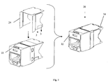
- jack assembly 20 includes jack 22 and an adhesively mounted foil label or shield 24.
- Jack 22 can be a CAT6A jack design, for example. Alternatively, other jacks such as CAT6, CAT7, or others can be used.
- jack assembly 26 which includes jack 22 and an adhesively mounted foil label 28 with extended sides 29.
- These foil labels 24, 28 are primarily used to reduce the amount of alien crosstalk occurring between neighboring jacks, as the level of coupling from non-neighboring jacks is already very low due to the fact that they are relatively far apart.
- jacks 20, 26 typically can include a wirecap as shown in Fig. 6 and other elements of Fig. 6 .
- the foil labels include an adhesive material with a metal liner, then a paint layer and protective coating, which is shown in Fig. 3 .
- the present invention reduces the mode conversion of the jack and improves alien crosstalk.
- a communication system 30 which can include communication cables, such as patch cables 32 and horizontal cables 33, connected to equipment 34.
- Equipment 34 is illustrated as a patch panel in Fig. 5 , but the equipment can be passive equipment or active equipment. Examples of passive equipment can be, but are not limited to, modular patch panels, punch-down patch panels, coupler patch panels, wall jacks, etc.
- Examples of active equipment can be, but are not limited to, Ethernet switches, routers, servers, physical layer management systems, and power-over-Ethernet equipment as can be found in data centers/telecommunications rooms; security devices (cameras and other sensors, etc.) and door access equipment; and telephones, computers, fax machines, printers and other peripherals as can be found in workstation areas.
- Communication system 30 can further include cabinets, racks, cable management and overhead routing systems, and other such equipment.
- Communication cables 32 and 33 are shown in the form of an unshielded twisted pair (UTP) cable, and more particularly a CAT6A cable which can operate at 10 Gb/s. However, the present invention can be applied to and/or implemented in connection with a variety of communications cables. Cables 33 can be terminated directly into equipment 34, or alternatively, can be terminated in a variety of punchdown or jack modules 40 such as RJ45 type, jack module cassettes, and many other connector types, or combinations thereof. Patch cables 32 are typically terminated in plugs 36.
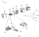
- Fig. 6 shows a more detailed exploded view of jack 40 which generally includes housing 42 that fits an RJ45 plug, a nose 44 that has eight PICs 56 that mate with a plug and wrap around sled 60, and interface with a rigid board 46.
- Rigid board 46 connects to IDCs 48, and rear sled 50 that holds the IDCs.
- a wire cap 52 allows for wires within cabling to connect with the IDCs, and this is also part of the jacks of Figs. 1-2 , although not shown in the views.
- Nose 44 includes a flex circuit board 54, plug interface contacts 56, front bottom sled 58 and front top sled 60.
- Figs. 1 and 2 are different from Fig.
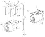
- foil label 70 in that they respectively show the two foil label designs 24, 28, whereas Fig. 6 illustrates an improved foil label 70 (see also Fig. 7 ) having a first side 72 and a mirror image second side 74, with a gap 76 therebetween.
- the design of rigid board 46 described herein works with all three of these foils 24, 28 and 70.
- foil label 70 includes extensions 78 that help reduce coupling between plugs and PICs in adjacent jacks.
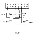
- Crosstalk compensation components can be included on both PICs 56 and flexible board 54, as shown in Fig. 8 and Figs. 9-10 , respectively.
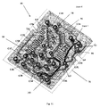
- rigid board 46 also includes crosstalk compensation components (either the same or opposite of polarity of plug crosstalk components), which are identified particularly in Fig. 12 , with the exception of C45.
- C45 improves return loss margin at higher frequencies in pair 4-5 by reducing the relatively high impedance of the second impedance region, as previously discussed. Although the return loss gets relatively worse at lower frequencies as a result of this modification, the overall margin improves over the frequency band of interest.
- Rigid board 46 includes lattice type compensation as also discussed in U.S. Provisional Patent Application Serial No. 61/090,403 .
- One of the novel aspects of the present invention is that it addresses a naturally unbalanced coupling which exists between all pairs and the foil label on the jack.
- the primary reason for this unbalance is shown in Fig. 6 .
- the IDCs 48 that are near the edge of the jack (pins 5, 2, 6, 7) capacitively couple more strongly to the foil than the IDCs 48 (pins 4, 1,3, 8) not near the edge of the jack. This is especially true on pair 4-5 and pair 1-2 where IDCs 5 and 2 are near the foil, and 1 and 4 are far away from it.
- rigid board 46 has four layers of conductive traces.
- the IDC vias receive and retain IDCs.
- the IDC vias are numbered 5-4-1-2 at the top of the board in Fig. 11 , and 7-8-3-6 on the bottom edge of the board, and are also plated through holes which interconnect some of the traces on the various layers.
- Signals or noise can couple relatively strongly to foil label 70, particularly through the IDC vias and IDCs 5, 2, 6, 7.
- IDC via 5 and IDC 5 are much closer to the foil label 70 than IDC via 4 and IDC 4 are.
- conductive trace stub 90 is routed close to the edge of board 46 near the foil 70 and is connected to trace 4 (a conductive trace interconnecting PIC via 4 with IDC via 4). Stub 90 thereby balances conductor 4 with respect to conductor 5 and the foil. Additionally and/or alternatively, trace 4 can be routed relatively close to the edge of rigid board 46 to increase the coupling to foil 70.
- stub 90 is 0.008 inches wide by 0.220 inches long in one half ounce copper (approximately 0.0007 inches thick), although other thicknesses, widths and lengths are possible.
- conductive trace stub 92 is routed close to the edge of board 46 near the foil 70 and connected to trace 1 (conductive trace interconnecting PIC via 1 with IDC via 1) via plated through hole 94.
- Stub 92 is similar to stub 90; however, because of space limitations on rigid board 46, stub 92 is only 0.005 inches wide by 0.075 inches long, also in one ounce copper (approximately 0.0014 inches thick plus additional plating to achieve a thickness between 0.002-0.0035), although other thicknesses, widths and lengths are possible.
- the 12 pair is further balanced by moving trace 1 very close to the board edge (closer to foil 70), and plated through hole 94 provides significant surface area in a third dimension (board thickness) which also capacitively couples to foil 70, giving stronger coupling between conductor 1 and the foil 70, thereby balancing the 12 pair with respect to foil 70.
- Unplated through holes generally at 96 reduce capacitance between traces 4 and 5 closer to the area of NEXT compensation to lessen the effects of compensation elements on return loss, by better impedance matching.
- Fig. 13 The result of the pair balancing with respect to the foil, and the use of a split foil is illustrated in Fig. 13 .
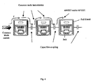
- the present invention achieves less common mode current 1' on the foil due to pair balancing relative to the foil, and the split foil eliminates the low-loss path for propagation of the common mode current from adjacent jack to adjacent jack.
- the overall improvement in alien crosstalk margin has been shown to be at least 4 dB with the improvements of the present invention.
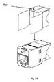
- the present invention can be used advantageously with each of the symmetric foil designs of Figs. 1 , 2 , 6 and 14 , although the designs of Figs. 1 and 2 would not have the characteristics and advantages of the split shield.
- Fig. 14 includes a continuous single piece foil with a gap in the metallization.
- through hole 100 (shown in Fig. 11 ) is meant to have the opposite effect as C45, and through hole 98 can be eliminated as unnecessary.
- the addition of capacitor C24 and elimination of C15 improves NEXT on pair combination 45-12, relative to the invention of U.S. Provisional Patent Application Serial No. 61/090,403 .
- Some other comparisons to U.S. Provisional Patent Application Serial No. 61/090,403 are as follows. Using inductive trace L3, along with the new inductor L3L, connects trace 3 to C38 and uses the lattice compensation and improves 36-78 NEXT. Changing the orientation of L6 to move it further away from the side of the rigid board reduces coupling to the foil. Moving the location of C58 and C16 better accommodates the new artwork of the present invention.
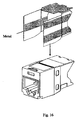
- Figs. 15-17 typically require modifications to the balance circuitry shown in Fig. 11 , such as smaller balance components on the side of rigid board 46 which have less, or no, conductive shielding. That is, smaller balance components are being provided on a particular portion of the rigid board that does not lie adjacent any conductive foil or shielding.
- each differential pair needs to achieve balance with each part of the foil so multiple foil parts require each foil part to be balanced with respect to the jack.
- Fig. 15 illustrates an embodiment of the foil label where one side does not have any metal (note that the embodiment shown here could be flipped so the opposite side is metalized);
- Fig. 16 illustrates an embodiment of the foil label with areas selectively chosen for metallization; and Fig.
- FIG. 17 illustrates an embodiment of the foil label which is an L-shaped metalized foil where one side of the jack and the top or base are covered by the foil leaving one side without any covering. Note that the embodiment shown in Fig. 17 can be modified by making the opposite side with a foil and the side shown in Fig. 17 removed.
- Alternative embodiments of the present invention include a jack with the circuit board of Fig. 11 , but with a capacitor C 15 between IDC vias 1 and 5, or a jack with the circuit board of Fig. 11 , but with capacitor C24 completely removed from the board along with any traces connected to it.
- Another alternative embodiment of the present invention eliminates the flex board.
Landscapes
- Details Of Connecting Devices For Male And Female Coupling (AREA)
- Coupling Device And Connection With Printed Circuit (AREA)
Claims (14)
- Fiche (40) comprenant :un boîtier (42) ;un(e) étiquette ou blindage de pellicule métallisée (70) entourant au moins partiellement le boîtier (42) ;une carte de circuit imprimé (46) ;des premier et deuxième contacts de déplacement d'isolation (48), le premier contact de déplacement d'isolation étant situé plus proche de l'étiquette ou du blindage de pellicule métallisée (70) que le deuxième contact de déplacement d'isolation, les premier et deuxième contacts de déplacement d'isolation (48) étant associés à un premier signal différentiel ;et caractérisée par :une première embase de piste conductrice (90) reliée au deuxième contact de déplacement d'isolation (48) et dirigée à proximité d'un bord de la carte de circuit imprimé (46) et de l'étiquette/blindage pelliculé(e) (70).
- Fiche (40) selon la revendication 1, comprenant en outre un premier trou de liaison associé au premier contact de déplacement d'isolation et un deuxième trou de liaison associé au deuxième contact de déplacement d'isolation.
- Fiche (40) selon la revendication 2, comprenant en outre un traineau (50).
- Fiche (40) selon la revendication 3, comprenant en outre un capuchon câblé (52).
- Fiche (40) selon la revendication 4, comprenant en outre des contacts d'interface de prise (56).
- Fiche (40) selon la revendication 1, comprenant en outre des pistes de signal sur la carte de circuit imprimé (46) associées au premier signal différentiel, une portion des pistes étant située proche d'un bord de la carte de circuit imprimé (46).
- Fiche (40) selon la revendication 2, comprenant en outre des pistes de signal sur la carte de circuit imprimé (46) associées au premier signal différentiel, une portion des pistes étant située proche d'un bord de la carte de circuit imprimé (46).
- Fiche (40) selon la revendication 1, comprenant en outre :des troisième et quatrième contacts de déplacement d'isolation (48), les troisième et quatrième contacts de déplacement d'isolation (48) étant associés à un second signal différentiel, le troisième contact de déplacement d'isolation étant plus proche de l'étiquette ou blindage de pellicule métallisée (70) que le quatrième contact de déplacement d'isolation ; etune seconde embase de piste conductrice (92) reliée au quatrième contact de déplacement d'isolation (92) et dirigée à proximité d'un bord de la carte de circuit imprimé (46) et de l'étiquette/blindage pelliculé(e) (70).
- Fiche (40) selon la revendication 8, comprenant en outre un troisième trou de liaison associé au troisième contact de déplacement d'isolation et un quatrième trou de liaison associé au quatrième contact de déplacement d'isolation.
- Fiche (40) selon la revendication 8, comprenant en outre un traineau (50).
- Fiche (40) selon la revendication 10, comprenant en outre un capuchon câblé (52).
- Fiche (40) selon la revendication 11, comprenant en outre des contacts d'interface de prise (56).
- Fiche (40) selon la revendication 8, comprenant en outre des pistes de signal sur la carte de circuit imprimé (46) associées au second signal différentiel, une portion des pistes étant située proche d'un bord de la carte de circuit imprimé (46).
- Fiche (40) selon la revendication 9, comprenant en outre des pistes de signal sur la carte de circuit imprimé (46) associées à la seconde paire de signaux différentiels, une portion des pistes étant située proche d'un bord de la carte de circuit imprimé (46
Applications Claiming Priority (3)
| Application Number | Priority Date | Filing Date | Title |
|---|---|---|---|
| US11923108P | 2008-12-02 | 2008-12-02 | |
| US12/628,732 US8167661B2 (en) | 2008-12-02 | 2009-12-01 | Method and system for improving crosstalk attenuation within a plug/jack connection and between nearby plug/jack combinations |
| PCT/US2009/066336 WO2010065588A1 (fr) | 2008-12-02 | 2009-12-02 | Procédé et système pour améliorer l'affaiblissement diaphonique dans une connexion prise/fiche et entre des combinaisons prise/fiche proches |
Publications (2)
| Publication Number | Publication Date |
|---|---|
| EP2371041A1 EP2371041A1 (fr) | 2011-10-05 |
| EP2371041B1 true EP2371041B1 (fr) | 2016-04-20 |
Family
ID=41559634
Family Applications (1)
| Application Number | Title | Priority Date | Filing Date |
|---|---|---|---|
| EP09796878.8A Active EP2371041B1 (fr) | 2008-12-02 | 2009-12-02 | Procédé et système pour améliorer l'affaiblissement diaphonique dans une connexion prise/fiche et entre des combinaisons prise/fiche proches |
Country Status (10)
| Country | Link |
|---|---|
| US (5) | US8167661B2 (fr) |
| EP (1) | EP2371041B1 (fr) |
| JP (2) | JP5209798B2 (fr) |
| KR (1) | KR101622117B1 (fr) |
| CN (1) | CN102232259B (fr) |
| AU (1) | AU2009322495B2 (fr) |
| BR (1) | BRPI0923135B1 (fr) |
| CA (1) | CA2745291C (fr) |
| MX (1) | MX2011005785A (fr) |
| WO (1) | WO2010065588A1 (fr) |
Cited By (1)
| Publication number | Priority date | Publication date | Assignee | Title |
|---|---|---|---|---|
| EP4538660A1 (fr) * | 2023-10-13 | 2025-04-16 | Hidria d.o.o. | Capteur de température |
Families Citing this family (80)
| Publication number | Priority date | Publication date | Assignee | Title |
|---|---|---|---|---|
| CN102124609B (zh) * | 2008-08-20 | 2013-09-11 | 泛达公司 | 具有多级补偿的高速连接器 |
| US8167661B2 (en) * | 2008-12-02 | 2012-05-01 | Panduit Corp. | Method and system for improving crosstalk attenuation within a plug/jack connection and between nearby plug/jack combinations |
| CN107069274B (zh) | 2010-05-07 | 2020-08-18 | 安费诺有限公司 | 高性能线缆连接器 |
| US8641452B2 (en) * | 2011-03-22 | 2014-02-04 | Panduit Corp. | Communication jack having an insulating element connecting a spring element and a spring end of a contact element |
| US9178314B2 (en) | 2011-05-31 | 2015-11-03 | Adder Technology Limited | Electronic device security |
| US8900015B2 (en) | 2011-10-03 | 2014-12-02 | Panduit Corp. | Communication connector with reduced crosstalk |
| US8858266B2 (en) | 2012-02-13 | 2014-10-14 | Sentinel Connector Systems, Inc. | High speed communication jack |
| US9337592B2 (en) | 2012-02-13 | 2016-05-10 | Sentinel Connector Systems, Inc. | High speed communication jack |
| US9627816B2 (en) | 2012-02-13 | 2017-04-18 | Sentinel Connector System Inc. | High speed grounded communication jack |
| US9653847B2 (en) | 2013-01-11 | 2017-05-16 | Sentinel Connector System, Inc. | High speed communication jack |
| TWI497843B (zh) * | 2012-04-17 | 2015-08-21 | Emcom Technology Inc | 電連接器 |
| US9136647B2 (en) | 2012-06-01 | 2015-09-15 | Panduit Corp. | Communication connector with crosstalk compensation |
| CN104704682B (zh) | 2012-08-22 | 2017-03-22 | 安费诺有限公司 | 高频电连接器 |
| US8961239B2 (en) | 2012-09-07 | 2015-02-24 | Commscope, Inc. Of North Carolina | Communication jack having a plurality of contacts mounted on a flexible printed circuit board |
| US9246463B2 (en) | 2013-03-07 | 2016-01-26 | Panduit Corp. | Compensation networks and communication connectors using said compensation networks |
| US8858268B2 (en) | 2013-03-14 | 2014-10-14 | Commscope, Inc. Of North Carolina | Communications plugs and patch cords with mode conversion control circuitry |
| US9257792B2 (en) | 2013-03-14 | 2016-02-09 | Panduit Corp. | Connectors and systems having improved crosstalk performance |
| US8858267B2 (en) | 2013-03-14 | 2014-10-14 | Commscope, Inc. Of North Carolina | Communications plugs and patch cords with mode conversion control circuitry |
| WO2014144735A1 (fr) * | 2013-03-15 | 2014-09-18 | Tyco Electronics Uk Ltd. | Connecteur avec compensation de diaphonie capacitive pour réduire une diaphonie étrangère |
| US9088106B2 (en) * | 2013-05-14 | 2015-07-21 | Commscope, Inc. Of North Carolina | Communications jacks having flexible printed circuit boards with common mode crosstalk compensation |
| CN110247219B (zh) | 2014-01-22 | 2021-06-15 | 安费诺有限公司 | 电连接器 |
| US9380710B2 (en) | 2014-01-29 | 2016-06-28 | Commscope, Inc. Of North Carolina | Printed circuit boards for communications connectors having openings that improve return loss and/or insertion loss performance and related connectors and methods |
| WO2015164538A1 (fr) * | 2014-04-23 | 2015-10-29 | Tyco Electronics Corporation | Connecteur électrique à capuchon de protection et à bornes protégées |
| BR112017006086A2 (pt) * | 2014-10-01 | 2017-12-19 | Sentinel Connector Systems Inc | tomada para comunicação em alta velocidade |
| US9966703B2 (en) | 2014-10-17 | 2018-05-08 | Panduit Corp. | Communication connector |
| CN105789930B (zh) * | 2014-12-16 | 2019-01-11 | 富士康(昆山)电脑接插件有限公司 | 线缆连接器组件及其制造方法 |
| JP6281481B2 (ja) | 2014-12-17 | 2018-02-21 | 株式会社オートネットワーク技術研究所 | コネクタ及び電線ユニット |
| US10050383B2 (en) * | 2015-05-19 | 2018-08-14 | Panduit Corp. | Communication connectors |
| US10547148B2 (en) | 2015-05-27 | 2020-01-28 | HD Networks, LLC | High-density data communications connection assembly |
| US9865976B2 (en) * | 2015-05-27 | 2018-01-09 | HD Networks, LLC | High-density data communications cable |
| US10177516B2 (en) | 2015-05-27 | 2019-01-08 | HD Networks, LLC | High-density bridge adapter |
| US10367321B2 (en) | 2015-05-27 | 2019-07-30 | HD Networks, LLC | High-density bridge adapter |
| CN108701922B (zh) | 2015-07-07 | 2020-02-14 | Afci亚洲私人有限公司 | 电连接器 |
| US9912083B2 (en) | 2015-07-21 | 2018-03-06 | Sentinel Connector Systems, Inc. | High speed plug |
| TWI754439B (zh) | 2015-07-23 | 2022-02-01 | 美商安芬諾Tcs公司 | 連接器、製造連接器方法、用於連接器的擴充器模組以及電子系統 |
| JP6655183B2 (ja) | 2015-11-11 | 2020-02-26 | ベル フューズ (マカオ コマーシャル オフショア) リミテッド | モジュラーコネクタ |
| US10637196B2 (en) * | 2015-11-11 | 2020-04-28 | Bel Fuse (Macao Commercial Offshore) Limited | Modular jack contact assembly having controlled capacitive coupling positioned within a jack housing |
| US20170245361A1 (en) * | 2016-01-06 | 2017-08-24 | Nokomis, Inc. | Electronic device and methods to customize electronic device electromagnetic emissions |
| WO2017136390A1 (fr) | 2016-02-02 | 2017-08-10 | Commscope Technologies Llc | Système de connecteur électrique pourvu de dispositifs de réduction de diaphonie étrangère |
| CA3021559A1 (fr) | 2016-05-04 | 2017-11-09 | Sentinel Connector Systems, Inc. | Fiche industrielle a grand conducteur |
| TWI743118B (zh) * | 2016-05-04 | 2021-10-21 | 美商哨兵連接器系統股份有限公司 | 高速通訊插座 |
| WO2018039164A1 (fr) * | 2016-08-23 | 2018-03-01 | Amphenol Corporation | Connecteur configurable pour hautes performances |
| CN209844139U (zh) * | 2016-10-07 | 2019-12-24 | 泛达公司 | 通信连接器 |
| US10361514B2 (en) * | 2017-03-02 | 2019-07-23 | Panduit Corp. | Communication connectors utilizing multiple contact points |
| CN118630506A (zh) | 2017-10-30 | 2024-09-10 | 安费诺富加宜(亚洲)私人有限公司 | 低串扰卡缘连接器 |
| US10601181B2 (en) | 2017-12-01 | 2020-03-24 | Amphenol East Asia Ltd. | Compact electrical connector |
| US10777921B2 (en) | 2017-12-06 | 2020-09-15 | Amphenol East Asia Ltd. | High speed card edge connector |
| US10530106B2 (en) | 2018-01-31 | 2020-01-07 | Bel Fuse (Macao Commercial Offshore) Limited | Modular plug connector with multilayer PCB for very high speed applications |
| US10840647B2 (en) * | 2018-06-08 | 2020-11-17 | Rockwell Automation Technologies, Inc. | PCB mounted connector with two-piece shield for improved ESD tolerance |
| CN208862209U (zh) | 2018-09-26 | 2019-05-14 | 安费诺东亚电子科技(深圳)有限公司 | 一种连接器及其应用的pcb板 |
| US11870171B2 (en) | 2018-10-09 | 2024-01-09 | Amphenol Commercial Products (Chengdu) Co., Ltd. | High-density edge connector |
| TWM576774U (zh) | 2018-11-15 | 2019-04-11 | 香港商安費諾(東亞)有限公司 | 具有防位移結構之金屬殼體及其連接器 |
| US11381015B2 (en) | 2018-12-21 | 2022-07-05 | Amphenol East Asia Ltd. | Robust, miniaturized card edge connector |
| US11189971B2 (en) | 2019-02-14 | 2021-11-30 | Amphenol East Asia Ltd. | Robust, high-frequency electrical connector |
| TWI889666B (zh) | 2019-02-19 | 2025-07-11 | 美商安芬諾股份有限公司 | 電連接器及用於製造電連接器之方法 |
| TWM582251U (zh) | 2019-04-22 | 2019-08-11 | 香港商安費諾(東亞)有限公司 | Connector set with built-in locking mechanism and socket connector thereof |
| TWI855075B (zh) | 2019-05-20 | 2024-09-11 | 美商安芬諾股份有限公司 | 連接器模組、連接器、電子組件、電連接器以及連接器模組的薄片 |
| TWI895292B (zh) | 2019-11-06 | 2025-09-01 | 香港商安費諾(東亞)有限公司 | 具有互鎖段之高頻率電連接器及製造其之方法 |
| US11588277B2 (en) | 2019-11-06 | 2023-02-21 | Amphenol East Asia Ltd. | High-frequency electrical connector with lossy member |
| US11031738B1 (en) * | 2020-01-03 | 2021-06-08 | Jyh Eng Technology Co., Ltd. | Multiple socket panel device with anti-crosstalk shielding structure |
| WO2021154702A1 (fr) | 2020-01-27 | 2021-08-05 | Fci Usa Llc | Connecteur à vitesse élevée |
| TWI887339B (zh) | 2020-01-27 | 2025-06-21 | 美商Fci美國有限責任公司 | 高速及高密度之直接耦合垂直式連接器 |
| TWM630230U (zh) | 2020-03-13 | 2022-08-01 | 大陸商安費諾商用電子產品(成都)有限公司 | 加強部件、電連接器、電路板總成及絕緣本體 |
| US11728585B2 (en) | 2020-06-17 | 2023-08-15 | Amphenol East Asia Ltd. | Compact electrical connector with shell bounding spaces for receiving mating protrusions |
| US11527839B2 (en) * | 2020-07-07 | 2022-12-13 | Panduit Corp. | T-splice connector |
| US11831092B2 (en) | 2020-07-28 | 2023-11-28 | Amphenol East Asia Ltd. | Compact electrical connector |
| US11652307B2 (en) | 2020-08-20 | 2023-05-16 | Amphenol East Asia Electronic Technology (Shenzhen) Co., Ltd. | High speed connector |
| CN212874843U (zh) | 2020-08-31 | 2021-04-02 | 安费诺商用电子产品(成都)有限公司 | 电连接器 |
| CN215816516U (zh) | 2020-09-22 | 2022-02-11 | 安费诺商用电子产品(成都)有限公司 | 电连接器 |
| CN213636403U (zh) | 2020-09-25 | 2021-07-06 | 安费诺商用电子产品(成都)有限公司 | 电连接器 |
| CN114498129A (zh) * | 2020-10-26 | 2022-05-13 | 富士康(昆山)电脑接插件有限公司 | 电连接器及应用于该连接器内的电路板 |
| CN112769003A (zh) * | 2020-12-26 | 2021-05-07 | 苏州浪潮智能科技有限公司 | 一种设置在pcb板上的网口以及服务器 |
| US11569613B2 (en) | 2021-04-19 | 2023-01-31 | Amphenol East Asia Ltd. | Electrical connector having symmetrical docking holes |
| US12176650B2 (en) | 2021-05-05 | 2024-12-24 | Amphenol East Asia Limited (Hong Kong) | Electrical connector with guiding structure and mating groove and method of connecting electrical connector |
| CN215266741U (zh) | 2021-08-13 | 2021-12-21 | 安费诺商用电子产品(成都)有限公司 | 一种满足高带宽传输的高性能卡类连接器 |
| US12592525B2 (en) | 2021-10-21 | 2026-03-31 | Amphenol Commercial Products (Chengdu) Co., Ltd. | High speed electrical connector |
| USD1067191S1 (en) | 2021-12-14 | 2025-03-18 | Amphenol Corporation | Electrical connector |
| USD1068685S1 (en) | 2021-12-14 | 2025-04-01 | Amphenol Corporation | Electrical connector |
| US12500379B2 (en) | 2022-03-31 | 2025-12-16 | Amphenol East Asia Limited (Hong Kong) | Electrical connector with segments having different widths |
| US12482974B2 (en) | 2022-03-31 | 2025-11-25 | Amphenol East Asia Limited (Hong Kong) | Multi-width electrical connector with recessed neck segment |
Family Cites Families (56)
| Publication number | Priority date | Publication date | Assignee | Title |
|---|---|---|---|---|
| JPS5055892A (fr) * | 1973-09-17 | 1975-05-16 | ||
| JPS5233091A (en) * | 1975-09-10 | 1977-03-12 | Hitachi Ltd | Connector |
| EP0205876A1 (fr) * | 1985-06-19 | 1986-12-30 | Siemens Aktiengesellschaft | Dispositif multipolaire enfichable comportant une réglette de positionnement avec un dispositif de blindage |
| US5044980A (en) * | 1990-01-16 | 1991-09-03 | Beta Phase, Inc. | High density and multiple insertion connector |
| US5030114A (en) * | 1990-04-30 | 1991-07-09 | International Business Machines Corporation | Shield overcoat |
| US5259770A (en) * | 1992-03-19 | 1993-11-09 | Amp Incorporated | Impedance controlled elastomeric connector |
| US5277625A (en) * | 1992-11-03 | 1994-01-11 | The Whitaker Corporation | Electrical connector with tape filter |
| US5256086A (en) * | 1992-12-04 | 1993-10-26 | Molex Incorporated | Electrical connector shield and method of fabricating same |
| NO314527B1 (no) * | 1995-09-29 | 2003-03-31 | Krone Gmbh | Koblingslist for höye overföringshastigheter |
| US5736910A (en) * | 1995-11-22 | 1998-04-07 | Stewart Connector Systems, Inc. | Modular jack connector with a flexible laminate capacitor mounted on a circuit board |
| CA2182438C (fr) * | 1996-07-31 | 2001-05-29 | Peter Craig | Connecteur de circuit |
| KR100287956B1 (ko) * | 1997-12-26 | 2001-09-17 | 이 은 신 | 비차폐 꼬임 케이블 접속용 차등모드 누화 억제장치 |
| FR2791816B1 (fr) * | 1999-04-01 | 2001-06-15 | Infra Sa | Connecteur male basse tension |
| JP3775163B2 (ja) * | 2000-03-31 | 2006-05-17 | 松下電工株式会社 | モジュラーコネクタ |
| US6585540B2 (en) * | 2000-12-06 | 2003-07-01 | Pulse Engineering | Shielded microelectronic connector assembly and method of manufacturing |
| US6572411B1 (en) * | 2001-11-28 | 2003-06-03 | Fci Americas Technology, Inc. | Modular jack with magnetic components |
| US6551139B1 (en) * | 2001-12-07 | 2003-04-22 | Hon Hai Precision Ind. Co., Ltd. | Electrical connector having shielding plate |
| DE60306389T2 (de) | 2002-08-19 | 2006-10-19 | Matsushita Electric Industrial Co., Ltd., Kadoma | Verfahren zur Bildung von Druckkontrolldaten |
| KR100510041B1 (ko) | 2002-11-21 | 2005-08-25 | 대은전자 주식회사 | 접속캡이 구비된 모듈러 잭 |
| US6726492B1 (en) * | 2003-05-30 | 2004-04-27 | Hon Hai Precision Ind. Co., Ltd. | Grounded electrical connector |
| JP4289606B2 (ja) * | 2003-08-22 | 2009-07-01 | 日本航空電子工業株式会社 | コネクタ |
| US7182649B2 (en) * | 2003-12-22 | 2007-02-27 | Panduit Corp. | Inductive and capacitive coupling balancing electrical connector |
| US7187766B2 (en) * | 2004-02-20 | 2007-03-06 | Adc Incorporated | Methods and systems for compensating for alien crosstalk between connectors |
| US7311550B2 (en) * | 2004-02-20 | 2007-12-25 | Adc Telecommunications, Inc. | Methods and systems for positioning connectors to minimize alien crosstalk |
| US7232340B2 (en) * | 2004-02-20 | 2007-06-19 | Adc Incorporated | Methods and systems for minimizing alien crosstalk between connectors |
| US7179115B2 (en) | 2004-04-26 | 2007-02-20 | Commscope Solutions Properties, Llc | Alien next compensation for adjacently placed connectors |
| CN100539323C (zh) * | 2004-06-10 | 2009-09-09 | 北卡罗来纳科姆斯科普公司 | 插座组件和用于制作该插座组件的方法 |
| US7083472B2 (en) * | 2004-06-10 | 2006-08-01 | Commscope Solutions Properties, Llc | Shielded jack assemblies and methods for forming a cable termination |
| US20060134995A1 (en) | 2004-12-17 | 2006-06-22 | Masud Bolouri-Saransar | Systems and methods for reducing crosstalk between communications connectors |
| US7033210B1 (en) * | 2004-12-27 | 2006-04-25 | Tyco Electronics Corporation | Signal conditioned modular jack assembly with improved shielding |
| US20060246784A1 (en) * | 2005-04-29 | 2006-11-02 | Aekins Robert A | Electrically isolated shielded connector system |
| CN101228672B (zh) * | 2005-06-14 | 2010-10-06 | 立维腾制造有限公司 | 连接器隔离屏蔽系统 |
| US7278879B2 (en) * | 2005-08-03 | 2007-10-09 | Leviton Manufacturing Co., Inc. | Connector isolation station system |
| WO2007044855A2 (fr) * | 2005-10-11 | 2007-04-19 | The Siemon Company | Plaquette de connexion blindee permettant de reduire la paradiaphonie etrangere |
| US7294024B2 (en) * | 2006-01-06 | 2007-11-13 | Adc Telecommunications, Inc. | Methods and systems for minimizing alien crosstalk between connectors |
| AU2006202309B2 (en) * | 2006-02-23 | 2011-03-24 | Surtec Industries, Inc. | Connector for communications systems having contact pin arrangement and compensation for improved performance |
| US7530854B2 (en) * | 2006-06-15 | 2009-05-12 | Ortronics, Inc. | Low noise multiport connector |
| US7288001B1 (en) * | 2006-09-20 | 2007-10-30 | Ortronics, Inc. | Electrically isolated shielded multiport connector assembly |
| JP5006618B2 (ja) * | 2006-10-25 | 2012-08-22 | イリソ電子工業株式会社 | コネクタ |
| KR20100074141A (ko) * | 2007-09-19 | 2010-07-01 | 레비톤 메뉴팩튜어링 캄파니 인코포레이티드 | 통신 콘센트 내에 위치된 플렉서블 인쇄회로보드 상에 형성되는 내부 누화 보상 회로와 이에 관련된 방법 및 시스템 |
| US7967645B2 (en) * | 2007-09-19 | 2011-06-28 | Leviton Manufacturing Co., Inc. | High speed data communications connector circuits, systems, and methods for reducing crosstalk in communications systems |
| US7946894B2 (en) * | 2007-10-04 | 2011-05-24 | Hubbell Incorporated | Alien crosstalk preventive cover |
| JP4375476B2 (ja) * | 2007-11-08 | 2009-12-02 | パナソニック電工株式会社 | モジュラジャック |
| CN102007651B (zh) * | 2007-12-19 | 2013-06-26 | 泛达公司 | 用于减少插头/插孔连接内产生共模信号的方法和系统 |
| US7798857B2 (en) * | 2008-02-12 | 2010-09-21 | Adc Gmbh | Asymmetric crosstalk compensation for improved alien crosstalk performance |
| US7575482B1 (en) * | 2008-04-22 | 2009-08-18 | Tyco Electronics Corporation | Electrical connector with enhanced back end design |
| IT1392143B1 (it) | 2008-09-15 | 2012-02-22 | Pompe Garbarino S P A | Pompa centrifuga multistadio con tamburo di bilanciamento idraulico a trafilamento controllato. |
| US8167661B2 (en) * | 2008-12-02 | 2012-05-01 | Panduit Corp. | Method and system for improving crosstalk attenuation within a plug/jack connection and between nearby plug/jack combinations |
| JP5136861B2 (ja) * | 2009-03-27 | 2013-02-06 | 住友電装株式会社 | シールドコネクタ |
| PL2415126T3 (pl) * | 2009-03-31 | 2016-06-30 | Fci Asia Pte Ltd | Ekranowane złącze o ulepszonym pozycjonowaniu ekranu |
| US7896692B2 (en) * | 2009-05-15 | 2011-03-01 | Leviton Manufacturing Co., Inc. | Method of improving isolation between circuits on a printed circuit board |
| US7857667B1 (en) * | 2009-11-19 | 2010-12-28 | Leviton Manufacturing Co., Inc. | Spring assembly with spring members biasing and capacitively coupling jack contacts |
| US7976349B2 (en) * | 2009-12-08 | 2011-07-12 | Commscope, Inc. Of North Carolina | Communications patching and connector systems having multi-stage near-end alien crosstalk compensation circuits |
| US7828603B1 (en) * | 2010-01-07 | 2010-11-09 | Yfc-Boneagle Electric Co., Ltd. | Electrical connector with crosstalk compensation |
| US7972150B1 (en) * | 2010-11-04 | 2011-07-05 | Jyh Eng Technology Co., Ltd. | Alien crosstalk preventive electrical socket, electrical plug and network cable |
| CN102394461B (zh) * | 2011-07-13 | 2013-10-09 | 台达电子企业管理(上海)有限公司 | 防电磁干扰插座的制造方法及防电磁干扰的插座 |
-
2009
- 2009-12-01 US US12/628,732 patent/US8167661B2/en not_active Expired - Fee Related
- 2009-12-02 AU AU2009322495A patent/AU2009322495B2/en active Active
- 2009-12-02 CN CN200980149115.4A patent/CN102232259B/zh active Active
- 2009-12-02 MX MX2011005785A patent/MX2011005785A/es active IP Right Grant
- 2009-12-02 KR KR1020117014164A patent/KR101622117B1/ko active Active
- 2009-12-02 EP EP09796878.8A patent/EP2371041B1/fr active Active
- 2009-12-02 CA CA2745291A patent/CA2745291C/fr active Active
- 2009-12-02 JP JP2011538733A patent/JP5209798B2/ja active Active
- 2009-12-02 BR BRPI0923135-8A patent/BRPI0923135B1/pt active IP Right Grant
- 2009-12-02 WO PCT/US2009/066336 patent/WO2010065588A1/fr not_active Ceased
-
2012
- 2012-03-28 US US13/432,969 patent/US8632362B2/en active Active
-
2013
- 2013-02-21 JP JP2013031799A patent/JP5623567B2/ja active Active
-
2014
- 2014-01-17 US US14/157,748 patent/US8979588B2/en active Active
-
2015
- 2015-03-13 US US14/657,399 patent/US9331431B2/en active Active
-
2016
- 2016-05-02 US US15/143,769 patent/US9991638B2/en active Active
Cited By (2)
| Publication number | Priority date | Publication date | Assignee | Title |
|---|---|---|---|---|
| EP4538660A1 (fr) * | 2023-10-13 | 2025-04-16 | Hidria d.o.o. | Capteur de température |
| WO2025078116A1 (fr) * | 2023-10-13 | 2025-04-17 | Hidria D.O.O. | Capteur de température |
Also Published As
| Publication number | Publication date |
|---|---|
| CN102232259B (zh) | 2014-06-18 |
| US20120184154A1 (en) | 2012-07-19 |
| US8979588B2 (en) | 2015-03-17 |
| KR101622117B1 (ko) | 2016-05-18 |
| JP5623567B2 (ja) | 2014-11-12 |
| HK1157074A1 (zh) | 2012-06-22 |
| US20100197162A1 (en) | 2010-08-05 |
| US20160248203A1 (en) | 2016-08-25 |
| AU2009322495A1 (en) | 2010-06-10 |
| MX2011005785A (es) | 2011-06-24 |
| US9331431B2 (en) | 2016-05-03 |
| US9991638B2 (en) | 2018-06-05 |
| JP2012510707A (ja) | 2012-05-10 |
| US20150188260A1 (en) | 2015-07-02 |
| EP2371041A1 (fr) | 2011-10-05 |
| CA2745291C (fr) | 2017-02-28 |
| CN102232259A (zh) | 2011-11-02 |
| US20140154919A1 (en) | 2014-06-05 |
| US8632362B2 (en) | 2014-01-21 |
| WO2010065588A1 (fr) | 2010-06-10 |
| CA2745291A1 (fr) | 2010-06-10 |
| KR20110096125A (ko) | 2011-08-29 |
| JP2013093335A (ja) | 2013-05-16 |
| BRPI0923135B1 (pt) | 2019-04-24 |
| US8167661B2 (en) | 2012-05-01 |
| JP5209798B2 (ja) | 2013-06-12 |
| AU2009322495B2 (en) | 2014-08-07 |
Similar Documents
| Publication | Publication Date | Title |
|---|---|---|
| EP2371041B1 (fr) | Procédé et système pour améliorer l'affaiblissement diaphonique dans une connexion prise/fiche et entre des combinaisons prise/fiche proches | |
| JP5377512B2 (ja) | プラグ/ジャック接続部内のコモンモード信号発生を低減するための方法およびシステム | |
| US8915756B2 (en) | Communication connector having a printed circuit board with thin conductive layers | |
| US7985103B2 (en) | Communication connector with improved crosstalk communication | |
| US7364470B2 (en) | Communications connectors with signal current splitting | |
| US7288001B1 (en) | Electrically isolated shielded multiport connector assembly | |
| HK1157074B (en) | Method and system for improving crosstalk attenuation within a plug/jack connection and between nearby plug/jack combinations | |
| HK1143705A (en) | Method and system for reducing common mode signal generation within a plug/jack connection | |
| HK1143705B (en) | Method and system for reducing common mode signal generation within a plug/jack connection |
Legal Events
| Date | Code | Title | Description |
|---|---|---|---|
| PUAI | Public reference made under article 153(3) epc to a published international application that has entered the european phase |
Free format text: ORIGINAL CODE: 0009012 |
|
| 17P | Request for examination filed |
Effective date: 20110629 |
|
| AK | Designated contracting states |
Kind code of ref document: A1 Designated state(s): AT BE BG CH CY CZ DE DK EE ES FI FR GB GR HR HU IE IS IT LI LT LU LV MC MK MT NL NO PL PT RO SE SI SK SM TR |
|
| DAX | Request for extension of the european patent (deleted) | ||
| REG | Reference to a national code |
Ref country code: HK Ref legal event code: DE Ref document number: 1157074 Country of ref document: HK |
|
| 17Q | First examination report despatched |
Effective date: 20120628 |
|
| GRAP | Despatch of communication of intention to grant a patent |
Free format text: ORIGINAL CODE: EPIDOSNIGR1 |
|
| INTG | Intention to grant announced |
Effective date: 20151022 |
|
| GRAS | Grant fee paid |
Free format text: ORIGINAL CODE: EPIDOSNIGR3 |
|
| GRAA | (expected) grant |
Free format text: ORIGINAL CODE: 0009210 |
|
| AK | Designated contracting states |
Kind code of ref document: B1 Designated state(s): AT BE BG CH CY CZ DE DK EE ES FI FR GB GR HR HU IE IS IT LI LT LU LV MC MK MT NL NO PL PT RO SE SI SK SM TR |
|
| REG | Reference to a national code |
Ref country code: GB Ref legal event code: FG4D |
|
| REG | Reference to a national code |
Ref country code: CH Ref legal event code: EP |
|
| REG | Reference to a national code |
Ref country code: AT Ref legal event code: REF Ref document number: 793346 Country of ref document: AT Kind code of ref document: T Effective date: 20160515 |
|
| REG | Reference to a national code |
Ref country code: IE Ref legal event code: FG4D |
|
| REG | Reference to a national code |
Ref country code: DE Ref legal event code: R096 Ref document number: 602009038047 Country of ref document: DE |
|
| REG | Reference to a national code |
Ref country code: LT Ref legal event code: MG4D |
|
| REG | Reference to a national code |
Ref country code: AT Ref legal event code: MK05 Ref document number: 793346 Country of ref document: AT Kind code of ref document: T Effective date: 20160420 |
|
| REG | Reference to a national code |
Ref country code: NL Ref legal event code: MP Effective date: 20160420 |
|
| PG25 | Lapsed in a contracting state [announced via postgrant information from national office to epo] |
Ref country code: PL Free format text: LAPSE BECAUSE OF FAILURE TO SUBMIT A TRANSLATION OF THE DESCRIPTION OR TO PAY THE FEE WITHIN THE PRESCRIBED TIME-LIMIT Effective date: 20160420 Ref country code: FI Free format text: LAPSE BECAUSE OF FAILURE TO SUBMIT A TRANSLATION OF THE DESCRIPTION OR TO PAY THE FEE WITHIN THE PRESCRIBED TIME-LIMIT Effective date: 20160420 Ref country code: LT Free format text: LAPSE BECAUSE OF FAILURE TO SUBMIT A TRANSLATION OF THE DESCRIPTION OR TO PAY THE FEE WITHIN THE PRESCRIBED TIME-LIMIT Effective date: 20160420 Ref country code: NL Free format text: LAPSE BECAUSE OF FAILURE TO SUBMIT A TRANSLATION OF THE DESCRIPTION OR TO PAY THE FEE WITHIN THE PRESCRIBED TIME-LIMIT Effective date: 20160420 Ref country code: NO Free format text: LAPSE BECAUSE OF FAILURE TO SUBMIT A TRANSLATION OF THE DESCRIPTION OR TO PAY THE FEE WITHIN THE PRESCRIBED TIME-LIMIT Effective date: 20160720 |
|
| PG25 | Lapsed in a contracting state [announced via postgrant information from national office to epo] |
Ref country code: GR Free format text: LAPSE BECAUSE OF FAILURE TO SUBMIT A TRANSLATION OF THE DESCRIPTION OR TO PAY THE FEE WITHIN THE PRESCRIBED TIME-LIMIT Effective date: 20160721 Ref country code: HR Free format text: LAPSE BECAUSE OF FAILURE TO SUBMIT A TRANSLATION OF THE DESCRIPTION OR TO PAY THE FEE WITHIN THE PRESCRIBED TIME-LIMIT Effective date: 20160420 Ref country code: ES Free format text: LAPSE BECAUSE OF FAILURE TO SUBMIT A TRANSLATION OF THE DESCRIPTION OR TO PAY THE FEE WITHIN THE PRESCRIBED TIME-LIMIT Effective date: 20160420 Ref country code: SE Free format text: LAPSE BECAUSE OF FAILURE TO SUBMIT A TRANSLATION OF THE DESCRIPTION OR TO PAY THE FEE WITHIN THE PRESCRIBED TIME-LIMIT Effective date: 20160420 Ref country code: PT Free format text: LAPSE BECAUSE OF FAILURE TO SUBMIT A TRANSLATION OF THE DESCRIPTION OR TO PAY THE FEE WITHIN THE PRESCRIBED TIME-LIMIT Effective date: 20160822 Ref country code: AT Free format text: LAPSE BECAUSE OF FAILURE TO SUBMIT A TRANSLATION OF THE DESCRIPTION OR TO PAY THE FEE WITHIN THE PRESCRIBED TIME-LIMIT Effective date: 20160420 Ref country code: LV Free format text: LAPSE BECAUSE OF FAILURE TO SUBMIT A TRANSLATION OF THE DESCRIPTION OR TO PAY THE FEE WITHIN THE PRESCRIBED TIME-LIMIT Effective date: 20160420 |
|
| REG | Reference to a national code |
Ref country code: FR Ref legal event code: PLFP Year of fee payment: 8 |
|
| PG25 | Lapsed in a contracting state [announced via postgrant information from national office to epo] |
Ref country code: IT Free format text: LAPSE BECAUSE OF FAILURE TO SUBMIT A TRANSLATION OF THE DESCRIPTION OR TO PAY THE FEE WITHIN THE PRESCRIBED TIME-LIMIT Effective date: 20160420 Ref country code: BE Free format text: LAPSE BECAUSE OF FAILURE TO SUBMIT A TRANSLATION OF THE DESCRIPTION OR TO PAY THE FEE WITHIN THE PRESCRIBED TIME-LIMIT Effective date: 20160420 |
|
| REG | Reference to a national code |
Ref country code: DE Ref legal event code: R097 Ref document number: 602009038047 Country of ref document: DE |
|
| PG25 | Lapsed in a contracting state [announced via postgrant information from national office to epo] |
Ref country code: CZ Free format text: LAPSE BECAUSE OF FAILURE TO SUBMIT A TRANSLATION OF THE DESCRIPTION OR TO PAY THE FEE WITHIN THE PRESCRIBED TIME-LIMIT Effective date: 20160420 Ref country code: SK Free format text: LAPSE BECAUSE OF FAILURE TO SUBMIT A TRANSLATION OF THE DESCRIPTION OR TO PAY THE FEE WITHIN THE PRESCRIBED TIME-LIMIT Effective date: 20160420 Ref country code: EE Free format text: LAPSE BECAUSE OF FAILURE TO SUBMIT A TRANSLATION OF THE DESCRIPTION OR TO PAY THE FEE WITHIN THE PRESCRIBED TIME-LIMIT Effective date: 20160420 Ref country code: RO Free format text: LAPSE BECAUSE OF FAILURE TO SUBMIT A TRANSLATION OF THE DESCRIPTION OR TO PAY THE FEE WITHIN THE PRESCRIBED TIME-LIMIT Effective date: 20160420 Ref country code: DK Free format text: LAPSE BECAUSE OF FAILURE TO SUBMIT A TRANSLATION OF THE DESCRIPTION OR TO PAY THE FEE WITHIN THE PRESCRIBED TIME-LIMIT Effective date: 20160420 |
|
| PLBE | No opposition filed within time limit |
Free format text: ORIGINAL CODE: 0009261 |
|
| STAA | Information on the status of an ep patent application or granted ep patent |
Free format text: STATUS: NO OPPOSITION FILED WITHIN TIME LIMIT |
|
| PG25 | Lapsed in a contracting state [announced via postgrant information from national office to epo] |
Ref country code: SM Free format text: LAPSE BECAUSE OF FAILURE TO SUBMIT A TRANSLATION OF THE DESCRIPTION OR TO PAY THE FEE WITHIN THE PRESCRIBED TIME-LIMIT Effective date: 20160420 |
|
| 26N | No opposition filed |
Effective date: 20170123 |
|
| REG | Reference to a national code |
Ref country code: HK Ref legal event code: GR Ref document number: 1157074 Country of ref document: HK |
|
| PG25 | Lapsed in a contracting state [announced via postgrant information from national office to epo] |
Ref country code: SI Free format text: LAPSE BECAUSE OF FAILURE TO SUBMIT A TRANSLATION OF THE DESCRIPTION OR TO PAY THE FEE WITHIN THE PRESCRIBED TIME-LIMIT Effective date: 20160420 |
|
| REG | Reference to a national code |
Ref country code: CH Ref legal event code: PL |
|
| PG25 | Lapsed in a contracting state [announced via postgrant information from national office to epo] |
Ref country code: MC Free format text: LAPSE BECAUSE OF FAILURE TO SUBMIT A TRANSLATION OF THE DESCRIPTION OR TO PAY THE FEE WITHIN THE PRESCRIBED TIME-LIMIT Effective date: 20160420 |
|
| REG | Reference to a national code |
Ref country code: IE Ref legal event code: MM4A |
|
| PG25 | Lapsed in a contracting state [announced via postgrant information from national office to epo] |
Ref country code: LU Free format text: LAPSE BECAUSE OF NON-PAYMENT OF DUE FEES Effective date: 20161202 Ref country code: CH Free format text: LAPSE BECAUSE OF NON-PAYMENT OF DUE FEES Effective date: 20161231 Ref country code: LI Free format text: LAPSE BECAUSE OF NON-PAYMENT OF DUE FEES Effective date: 20161231 |
|
| PG25 | Lapsed in a contracting state [announced via postgrant information from national office to epo] |
Ref country code: IE Free format text: LAPSE BECAUSE OF NON-PAYMENT OF DUE FEES Effective date: 20161202 |
|
| REG | Reference to a national code |
Ref country code: FR Ref legal event code: PLFP Year of fee payment: 9 |
|
| PG25 | Lapsed in a contracting state [announced via postgrant information from national office to epo] |
Ref country code: HU Free format text: LAPSE BECAUSE OF FAILURE TO SUBMIT A TRANSLATION OF THE DESCRIPTION OR TO PAY THE FEE WITHIN THE PRESCRIBED TIME-LIMIT; INVALID AB INITIO Effective date: 20091202 Ref country code: CY Free format text: LAPSE BECAUSE OF FAILURE TO SUBMIT A TRANSLATION OF THE DESCRIPTION OR TO PAY THE FEE WITHIN THE PRESCRIBED TIME-LIMIT Effective date: 20160420 |
|
| PG25 | Lapsed in a contracting state [announced via postgrant information from national office to epo] |
Ref country code: TR Free format text: LAPSE BECAUSE OF FAILURE TO SUBMIT A TRANSLATION OF THE DESCRIPTION OR TO PAY THE FEE WITHIN THE PRESCRIBED TIME-LIMIT Effective date: 20160420 Ref country code: IS Free format text: LAPSE BECAUSE OF FAILURE TO SUBMIT A TRANSLATION OF THE DESCRIPTION OR TO PAY THE FEE WITHIN THE PRESCRIBED TIME-LIMIT Effective date: 20160420 Ref country code: MK Free format text: LAPSE BECAUSE OF FAILURE TO SUBMIT A TRANSLATION OF THE DESCRIPTION OR TO PAY THE FEE WITHIN THE PRESCRIBED TIME-LIMIT Effective date: 20160420 |
|
| PG25 | Lapsed in a contracting state [announced via postgrant information from national office to epo] |
Ref country code: BG Free format text: LAPSE BECAUSE OF FAILURE TO SUBMIT A TRANSLATION OF THE DESCRIPTION OR TO PAY THE FEE WITHIN THE PRESCRIBED TIME-LIMIT Effective date: 20160420 |
|
| PG25 | Lapsed in a contracting state [announced via postgrant information from national office to epo] |
Ref country code: MT Free format text: LAPSE BECAUSE OF NON-PAYMENT OF DUE FEES Effective date: 20161202 |
|
| REG | Reference to a national code |
Ref country code: DE Ref legal event code: R082 Ref document number: 602009038047 Country of ref document: DE Representative=s name: KILBURN & STRODE LLP, NL |
|
| PGFP | Annual fee paid to national office [announced via postgrant information from national office to epo] |
Ref country code: GB Payment date: 20251229 Year of fee payment: 17 |
|
| PGFP | Annual fee paid to national office [announced via postgrant information from national office to epo] |
Ref country code: FR Payment date: 20251226 Year of fee payment: 17 |
|
| PGFP | Annual fee paid to national office [announced via postgrant information from national office to epo] |
Ref country code: DE Payment date: 20251229 Year of fee payment: 17 |