EP2371419A2 - Conduite électrique d'un condensateur pour implants médicaux et procédé de fabrication et d'utilisation de celle-ci - Google Patents
Conduite électrique d'un condensateur pour implants médicaux et procédé de fabrication et d'utilisation de celle-ci Download PDFInfo
- Publication number
- EP2371419A2 EP2371419A2 EP11156794A EP11156794A EP2371419A2 EP 2371419 A2 EP2371419 A2 EP 2371419A2 EP 11156794 A EP11156794 A EP 11156794A EP 11156794 A EP11156794 A EP 11156794A EP 2371419 A2 EP2371419 A2 EP 2371419A2
- Authority
- EP
- European Patent Office
- Prior art keywords
- pin
- capacitor
- aluminum
- glass solder
- flange
- Prior art date
- Legal status (The legal status is an assumption and is not a legal conclusion. Google has not performed a legal analysis and makes no representation as to the accuracy of the status listed.)
- Withdrawn
Links
Images


Classifications
-
- A—HUMAN NECESSITIES
- A61—MEDICAL OR VETERINARY SCIENCE; HYGIENE
- A61N—ELECTROTHERAPY; MAGNETOTHERAPY; RADIATION THERAPY; ULTRASOUND THERAPY
- A61N1/00—Electrotherapy; Circuits therefor
- A61N1/18—Applying electric currents by contact electrodes
- A61N1/32—Applying electric currents by contact electrodes alternating or intermittent currents
- A61N1/36—Applying electric currents by contact electrodes alternating or intermittent currents for stimulation
- A61N1/372—Arrangements in connection with the implantation of stimulators
- A61N1/375—Constructional arrangements, e.g. casings
- A61N1/3752—Details of casing-lead connections
- A61N1/3754—Feedthroughs
-
- Y—GENERAL TAGGING OF NEW TECHNOLOGICAL DEVELOPMENTS; GENERAL TAGGING OF CROSS-SECTIONAL TECHNOLOGIES SPANNING OVER SEVERAL SECTIONS OF THE IPC; TECHNICAL SUBJECTS COVERED BY FORMER USPC CROSS-REFERENCE ART COLLECTIONS [XRACs] AND DIGESTS
- Y10—TECHNICAL SUBJECTS COVERED BY FORMER USPC
- Y10T—TECHNICAL SUBJECTS COVERED BY FORMER US CLASSIFICATION
- Y10T29/00—Metal working
- Y10T29/49—Method of mechanical manufacture
- Y10T29/49002—Electrical device making
- Y10T29/49117—Conductor or circuit manufacturing
- Y10T29/49124—On flat or curved insulated base, e.g., printed circuit, etc.
- Y10T29/49155—Manufacturing circuit on or in base
- Y10T29/49165—Manufacturing circuit on or in base by forming conductive walled aperture in base
Definitions
- the invention relates to a so-called implementation (the pin area) of an electrolytic, tantalum, niobium or other capacitor. It further relates to a method of making and using such a bushing, and to a capacitor having such bushing.
- Capacitors such as electrolytic, tantalum or niobium capacitors for use in medical electronic implants, such as defibrillators, are known in various designs and in practical use. Supports based on Al foils for high-voltage applications, so-called Al-HV capacitors, are commercially available in consumer electronics. They have a seal made of rubber-like substances or plastics, which, however, does not prevent a (very slow) escape of electrolyte components from the interior of the capacitor to the outside. This results in a limited life and reliability and the risk of contamination of the interior of devices in which they are installed, so specifically of said implants. Also known are structures based on tantalum or niobium, so-called Ta- or Nb-HV capacitors, but which are much heavier compared to Al-HV capacitors and their manufacturing technology is difficult to control.
- the invention has for its object to provide an improved structure for electrolytic capacitors of the Al-HV type as well as for the other mentioned Ta-, Nb or other types of capacitors, which gives this particular improved reliability, longer life and improved usability in medical electronic implants ,
- the invention includes the essential idea to perform the generic implementation hermetically sealed, the implementation of the condenser inside hermetically sealed relative to the outside of the capacitor. It further includes the idea of providing a glass solder plug electrically insulating the terminal pin from the aluminum flange.
- the connection pin is designed to be compatible with the inside of the capacitor at least at a section located inside the capacitor.
- an expedient embodiment of the invention provides that the connecting pin in the region of its length in which it is in contact with the glass solder plug, at least one core of a material having approximately the same or a smaller coefficient of thermal expansion as the glass solder , As a result, unacceptably high mechanical tensile stresses in the glass solder during the manufacture and use of the manufactured implementation can be avoided in principle.
- the lead pin or its core may be made of Pt, Pt / Ir, FeNi, FeNiCo, FeCr, Nb, Ta, Mo, W, Cr, FeCr in the region of its length in contact with the glass solder plug. V, Ti and other metals or their alloys.
- the portion of the connecting pin inside the electrolytic capacitor which is important for electrochemistry is an aluminum pin, an aluminum sheet or an aluminum foil.
- the aluminum pin, the aluminum sheet or the aluminum foil is electrically conductively attached to a portion of the connecting pin of a different material, in particular soldered, welded, infected, crimped or glued electrically conductive.
- Aluminum as the internal material of the terminal pin is fully compatible with the rest of the structure of an Al-HV capacitor and free from interfering ion leakage effects.
- an embodiment is useful in which a pin of Pt, Pt / Ir, FeNi, FeNiCo, FeCr, Nb, Ta, Mo, W, Cr, FeCr, V, Ti and other metals or their alloys are added to the aluminum pin or the aluminum sheet, in particular soldered, welded, infected, crimped or glued.
- the outside connecting pin may have a so-called nailhead, be flattened, curved, provided with an attached sleeve or disk, or otherwise designed to be suitable.
- the Nailhead facilitates subsequent soldering of the external connection, especially by means of a reflow process.
- Another preferred construction of the proposed implementation is characterized in that the connecting pin in the aluminum flange of a ceramic ring, in particular of Al 2 O 3 ceramic, surrounded, so that the ceramic ring for the glass solder plug during the soldering process forms a conclusion and the glass profile thus positively influenced, so that the glass solder graft can achieve a hermetic seal in the production of the implementation with a higher yield.
- a combined glass-ceramic bushing is additionally given a high mechanical stability by the highly rigid ceramic component, and the ceramic component also realizes a high-quality and reliable electrical insulation gap on the adjacent surfaces of the (aluminum) flange and connecting pin. In particular, it provides the glass solder plug mechanical protection against lateral forces (bending forces) that can attack the pin.
- a filler or a coating surrounding the connecting pin is provided on the inside of the glass solder plug.
- the filler or coating is dimensioned and arranged such that it masks a joint in the pin when the joint is incompatible with the interior of the capacitor and can not be sufficiently separated from the capacitor interior by the glass solder plug. If the glass solder graft itself is incompatible with the condenser interior, then the filler or coating will cover the surface of the glass solder graft accessible to the condenser interior.
- This filler or this coating ensures the important for the function of the capacitor compatibility between the materials present in its interior, which would not be guaranteed by the outside to achieve hermetic tightness to be used materials.
- the filler may also be present as a plug, but also as a coating, coating vapor deposition o. ⁇ ., And should cover all incompatible with the interior materials surfaces.
- a convenient process procedure for the production of the implementation which specifically allows the use of pin materials with a significantly different thermal expansion coefficient from the glass solder, is characterized in that during the production of the glass solder graft, the pin is cooled by means of a heat sink.
- the heat input into the glass solder for example, by IR radiation (such as a CO 2 laser or inductive heat coupling via the surrounding flange o. ⁇ . Made.
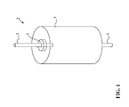
- Fig. 1 shows a perspective view of a known design of an electrolytic capacitor 1 with two pins 3 and 4, wherein a sketch 5 is shown in dashed lines on an end face of a housing 7.
- Fig. 2 shows as an embodiment of the invention, a passage 20 with an aluminum pin (pin) 21, an upper and lower side provided with flat cylindrical recesses Al flange 23 and each lying in the Al flange 23 ceramic discs 25a, 25b with a central opening to Passage of the Al-pin 21.
- pin aluminum pin
- Fig. 2 shows as an embodiment of the invention, a passage 20 with an aluminum pin (pin) 21, an upper and lower side provided with flat cylindrical recesses Al flange 23 and each lying in the Al flange 23 ceramic discs 25a, 25b with a central opening to Passage of the Al-pin 21.
- the Al-flange 23 connects to the structure of a (not shown here) housing wall, and between the middle part of the Al-flange 23 and the inner walls of the central openings of the ceramic discs 25a, 25b and the outer surface of the pin 21 is a glass solder plug 27, which seals both the pin 21 and the Al flange 23 hermetically against the surrounding surfaces, so that the overall result is a hermetic seal between the condenser interior and exterior, which also with a high Yield mechanically stable, electrically insulating, dimensionally stable, long-term stable and geometrically compact.
- a low-melting glass solder with a melting temperature significantly below that of aluminum (660 ° C) to use such as a lead-containing solder type G 017-052 Schott, with a soldering temperature of about 410 ° C or a lead-free solder of G 018-249, also from Schott, with a soldering temperature of 500 ° C.
- Stress due to the different thermal expansion coefficients of the Al-pin and Al-flange on the one hand and the glass solder on the other hand can largely be avoided by the special structural design, which includes the use of a very small amount of glass to produce the glass solder plug 27.
- a cooling of the pin 21 via a heat sink to be considered useful in this sense.
- Fig. 3 shows one of the execution Fig. 2 basically similar construction of another implementation 30. Same or similar parts are with Fig. 2 ajar reference numerals and will not be explained again here.
- the main difference from the execution after Fig. 2 consists in the use of a pin 31 of platinum.
- This pin is provided with an Al coating 31a that includes at least the capacitor inner portion of the pin and the inside portion of the glass plug 37.
- the coating can also - as in Fig. 3 indicated - extend into the condenser outer region of the pin, for example, to not affect the electrochemical processes in the glass solder, which play a role during the Hochtemperaturverlötung.
- the terminal pin With this construction of the terminal pin, on the one hand, it is better adapted to the coefficient of thermal expansion of the glass, and on the other hand the exposure of surfaces incompatible with the other materials inside the capacitor is avoided by the Al coating.
- the Al coating can be provided in the capacitor with an adequate oxide layer, and from the outside of the pin soldering, welding, clip-on, ancrimp- or electrically conductive attachable.
- Fig. 4 shows as training of in Fig. 3 shown execution another implementation 40, where in turn Fig. 2 or 3 reference numerals are used.
- the adjacent sections of the housing 7 are shown in this illustration, which are gas-tightly connected via a weld 7a with the Al flange 43.
- the figure shows an Al capacitor plate 9, which forms an essential functional component of the capacitor structure, as well as joining or welding points 9a for its connection to the connecting pin.
- the pin here from an outer pin 41 made of a material other than Al, z.
- a material other than Al z.
- Pt, Pt / Ir, FeNi, FeNiCo, FeCr, Nb, Ta, Mo, W, Cr, FeCr, V or Ti and an inner pin 41 'made of Al, which are connected to each other via welds 41b.
- the entire capacitor inner surface of both partial connection pins 41, 41 'and the surface of the welding points 41b is covered with an Al coating 41a compatible with the capacitor interior.
- FIG. 5 shows another feedthrough 50 according to the invention with a composite pin 51/51 'of a first pin portion 51 of Pt, Pt / Ir, FeNi, FeNiCo, FeCr, Nb, Ta, Mo, W, Cr, FeCr, V or Ti or an alloy of these or a similar material and a second pin portion 51 'of aluminum. Both sections are connected by a joint 51b, which is realized by welding, soldering, crimping, electrically conductive bonding or another suitable method.
- At least the joint and the adjoining part of the pin and the transition to the exposed surface of the glass plug is covered by a filler plug and thus protected the capacitor interior from incompatible components.
- the filler graft can also be designed as a comparatively thin, volume-saving coating which prevents inadmissible ion exchange of the incompatible constituents with the condenser interior. If the glass plug is made of a compatible material relative to the condenser interior, then it need not be completely covered by the filler plug or coating.
- the joint and, in addition, part of the Al pin portion may be partially or completely enclosed by the glass plug.
- the glass plug due to the comparatively large thermal expansion coefficients of the joint and the pin generally ensure no hermetically sealed closure of these parts relative to the capacitor interior.
- This object should be taken over in a preferred design variant by a filler graft or by a corresponding coating which completely covers at least the transition from the glass plug to the pin or to the joint and thus masked with respect to the capacitor interior.
- two ceramic rings enclose the glass plug externally and internally, wherein the two-part pin is guided through an opening of the ceramic rings and is hermetically sealed by the glass plug.
- the joint may be wholly or partially within the glass plug and completely or partially within the ceramic ring located in the condenser interior.
- the inner ceramic ring and the flange, as well as the housing may be completely or partially covered or wetted by the filler graft or the coating.
- Fig. 6 shows a slight modification of the in Fig. 5 illustrated construction 60, in which the filler plug 69, the bore of the flange 53 completely fills and wets a larger portion of the inner terminal pin portion 61 '.
- This has the advantage that the joint 61b between the pin portions 61 and 61 'need not be within the bore of the flange 63 and therefore can be more easily formed.
- the joint may also be a welding or soldering or electrically conductive adhesive bond, or the pin portions may be crimped together (via an additional element or via an opening (bore) or a gap of the two pins).
- Embodiment 70 shows a minor modification of FIGS Fig. 6 shown embodiment, in which provided in the upper surface of the flange 73, an enlarged recess and in this the ceramic disk 75 is inserted such that its upper end surface is approximately flush with the upper end face of the flange 73 and thus a total (including the upper housing section 7) a substantially planar surface of the passage and the associated condenser end face is provided.
- this principle can be transferred with the ceramic disc inserted on a located on the inside of the capacitor ceramic disc.
- the ceramic disc (s) provided with a central opening takes on the task of centering the pin relative to the central flange opening during the soldering of the glass / ceramic bushing in the production process.
- the flange 83 has a further modified shape, a discontinuation of the proposed in the other embodiments ceramic disc (s) allows.
- this here has an inwardly facing tapered portion 83 a, which positions the glass solder plug during the manufacturing process and in the application to some extent the mechanical function of the ceramic disc takes over.
- the inner portion 81 'of the terminal pin is here as a design variant wider (or thicker) than the outer pin portion 81, in the area of the hermetically sealed seal is made on the glass solder.
- the inner portion may also be a sheet of various shapes or the like.
- the beveled portion 83 a can be omitted in a further design variant and the flange thus have a stepless, cylindrical opening, in which case by appropriate measures during the manufacturing process, such.
- the position of the glass solder plug is set in the opening of the flange.
- Fig. 9 shows a further embodiment of a passage 90, in which the ceramic disc 95 is mounted flat on the surface of the flange 93.
- the inner portion 91 'of the terminal pin is wider (and / or thicker) than the outer pin portion 91 constructed.
- the inner portion 91 ' has a tapered portion to the joint 91b.
- the joint 91b also lies here within the glass solder plug 97, which completely surrounds the joint 91b.
- a filler plug covers the environment in the nutrient and / or around the joint 91b, but the flange opening of the flange 93 is not completely filled by the filler plug.
- the glass solder plug 97 and / or filler plug 99 may be formed of a material compatible with the condenser interior to protect the condenser interior (eg, the electrolyte) from incompatible components outside the condenser.
- Fig. 10 shows an alternative to the embodiment Fig. 9 ,
- a bushing 100 is shown, which has a recess on the surface of the flange 103, in which the ceramic disc 105 is inserted.
- the passage 100 is then shaped so that the outer surface of the ceramic disc 105 with the surface of the flange 103rd lie flush.
- the inner portion 101 'of the terminal pin is wider (and / or thicker) than the outer pin portion 101 constructed.
- the inner portion 101 ' has a chamfered portion to the joint 101b.
- the joint 101b is located here within the glass solder plug 107, which completely surrounds the joint 101b.
- the filler plug is replaced by a thin coating 108 which completely covers the glass solder plug 107.
- the filler plug 107 may be formed of a material compatible with the condenser interior to protect the condenser interior (eg, the electrolyte) from incompatible components outside the condenser. Thus, space is saved within the capacitor and it is avoided inadmissible ion exchange with incompatible component with the capacitor interior.
- the filler layer may be, for example, rubber, a silicone compound a halogen- or chlorine-free plastic or polymers such as epoxy resin, polyimide (for example Kapton®) or Perylene®.
- Fig. 11 shows a further alternative of the implementation s, which on the embodiments of the Fig. 9 or 10 based.
- the filler coating 108 or the filler graft 99 was completely dispensed with.
- the glass solder plug 117 is formed from a material compatible with the capacitor interior.
- the filler can be dispensed with in the form of either a graft or a coating, and yet the condenser interior (for example, the electrolyte) can be protected from incompatible components outside the condenser.
- the glass solder plug 117 encloses the joint 111b, by means of which the inner portion 111 'and the outer portion 111 of the terminal pin is electrically connected to each other. Due to the complete enclosure of the joint 117, it is protected from the medium in the condenser interior.
Landscapes
- Health & Medical Sciences (AREA)
- Engineering & Computer Science (AREA)
- Biomedical Technology (AREA)
- Nuclear Medicine, Radiotherapy & Molecular Imaging (AREA)
- Radiology & Medical Imaging (AREA)
- Life Sciences & Earth Sciences (AREA)
- Animal Behavior & Ethology (AREA)
- General Health & Medical Sciences (AREA)
- Public Health (AREA)
- Veterinary Medicine (AREA)
- Fixed Capacitors And Capacitor Manufacturing Machines (AREA)
- Electrotherapy Devices (AREA)
Applications Claiming Priority (1)
| Application Number | Priority Date | Filing Date | Title |
|---|---|---|---|
| US31840310P | 2010-03-29 | 2010-03-29 |
Publications (2)
| Publication Number | Publication Date |
|---|---|
| EP2371419A2 true EP2371419A2 (fr) | 2011-10-05 |
| EP2371419A3 EP2371419A3 (fr) | 2014-10-29 |
Family
ID=44288094
Family Applications (1)
| Application Number | Title | Priority Date | Filing Date |
|---|---|---|---|
| EP11156794.7A Withdrawn EP2371419A3 (fr) | 2010-03-29 | 2011-03-25 | Conduite électrique d'un condensateur pour implants médicaux et procédé de fabrication et d'utilisation de celle-ci |
Country Status (2)
| Country | Link |
|---|---|
| US (1) | US8675338B2 (fr) |
| EP (1) | EP2371419A3 (fr) |
Cited By (4)
| Publication number | Priority date | Publication date | Assignee | Title |
|---|---|---|---|---|
| DE102014016600A1 (de) * | 2014-11-11 | 2016-05-12 | Schott Ag | Durchführung |
| WO2023138843A1 (fr) * | 2022-01-21 | 2023-07-27 | Schott Ag | Traversée électrique et accumulateur d'énergie doté d'une telle traversée |
| DE202023103813U1 (de) | 2023-07-07 | 2024-10-10 | Schott Ag | Elektrische Durchführung und Energiespeicher mit einer solchen Durchführung |
| DE102023118080A1 (de) | 2023-07-07 | 2025-01-09 | Schott Ag | Elektrische Durchführung und Energiespeicher mit einer solchen Durchführung |
Families Citing this family (8)
| Publication number | Priority date | Publication date | Assignee | Title |
|---|---|---|---|---|
| US9345895B2 (en) | 2012-04-26 | 2016-05-24 | Medtronic, Inc. | Implantable medical device and feedthrough and method of making same |
| US9119970B2 (en) * | 2013-08-19 | 2015-09-01 | Boston Scientific Neuromodulation Corporation | Feedthrough assembly with glass layer and electrical stimulation systems containing the assembly |
| KR101656723B1 (ko) * | 2015-06-30 | 2016-09-12 | 재단법인 오송첨단의료산업진흥재단 | 피드스루 제조방법 |
| WO2018000074A1 (fr) * | 2016-06-27 | 2018-01-04 | Volvo Group Canada Inc. | Dispositif d'étanchéité de câble pour boîte de jonction électrique |
| US10510998B2 (en) * | 2017-02-01 | 2019-12-17 | Pacesetter, Inc. | Electrode feedthru having pin attached to wire therein and method of manufacturing |
| US11024445B2 (en) | 2018-09-14 | 2021-06-01 | Volt Holdings, LLC | Power cable with an overmolded probe for power transfer to a non-thermal plasma generator and a method for constructing the overmolded probe |
| US12094661B2 (en) * | 2022-01-25 | 2024-09-17 | Medtronic, Inc. | Feedthrough ferrule with beveled ledge |
| CN121263905A (zh) * | 2023-05-24 | 2026-01-02 | 肖特股份有限公司 | 用于电气装置的带有电气馈通件的壳体部件和具有这种壳体部件的储能器 |
Citations (2)
| Publication number | Priority date | Publication date | Assignee | Title |
|---|---|---|---|---|
| US20050007718A1 (en) * | 2003-02-27 | 2005-01-13 | Stevenson Robert A. | EMI filter terminal assembly with wire bond pads for human implant applications |
| EP1897589A2 (fr) * | 2006-09-07 | 2008-03-12 | BIOTRONIK CRM Patent AG | Passage électrique |
Family Cites Families (13)
| Publication number | Priority date | Publication date | Assignee | Title |
|---|---|---|---|---|
| US5333095A (en) * | 1993-05-03 | 1994-07-26 | Maxwell Laboratories, Inc., Sierra Capacitor Filter Division | Feedthrough filter capacitor assembly for human implant |
| US5734546A (en) * | 1994-09-21 | 1998-03-31 | Rohm Co. Ltd. | Capacitor element for solid electrolytic capacitor and process for making the same |
| US5870272A (en) * | 1997-05-06 | 1999-02-09 | Medtronic Inc. | Capacitive filter feedthrough for implantable medical device |
| EP1109180B1 (fr) * | 1999-12-14 | 2012-02-08 | Greatbatch Ltd. | Anschlussanordnung für EMI-Durchführungsfilter |
| US6414835B1 (en) * | 2000-03-01 | 2002-07-02 | Medtronic, Inc. | Capacitive filtered feedthrough array for an implantable medical device |
| US6498951B1 (en) * | 2000-10-13 | 2002-12-24 | Medtronic, Inc. | Implantable medical device employing integral housing for a formable flat battery |
| EP1488434B1 (fr) * | 2002-02-28 | 2012-12-12 | Greatbatch Ltd. | Ensemble borne de filtrage de passage anti-interference electromagnetique pour fixation electrique entre fils de sortie et condensateur |
| US6801424B1 (en) * | 2003-05-30 | 2004-10-05 | Medtronic, Inc. | Electrolytic capacitor for use in an implantable medical device |
| US7966070B2 (en) * | 2003-09-12 | 2011-06-21 | Medtronic, Inc. | Feedthrough apparatus with noble metal-coated leads |
| US6903268B2 (en) * | 2003-10-29 | 2005-06-07 | Medtronic, Inc. | Implantable device feedthrough assembly |
| EP1883940A2 (fr) * | 2005-05-06 | 2008-02-06 | David H. Stark | Unites de vitrage isole et procedes correspondants |
| US8326425B2 (en) * | 2006-03-30 | 2012-12-04 | Cardiac Pacemakers, Inc. | Feedthrough connector for implantable device |
| CN102037528A (zh) * | 2008-03-20 | 2011-04-27 | 格瑞巴奇有限公司 | 屏蔽三端子平通emi/消能滤波器 |
-
2011
- 2011-03-25 US US13/071,974 patent/US8675338B2/en not_active Expired - Fee Related
- 2011-03-25 EP EP11156794.7A patent/EP2371419A3/fr not_active Withdrawn
Patent Citations (2)
| Publication number | Priority date | Publication date | Assignee | Title |
|---|---|---|---|---|
| US20050007718A1 (en) * | 2003-02-27 | 2005-01-13 | Stevenson Robert A. | EMI filter terminal assembly with wire bond pads for human implant applications |
| EP1897589A2 (fr) * | 2006-09-07 | 2008-03-12 | BIOTRONIK CRM Patent AG | Passage électrique |
Cited By (7)
| Publication number | Priority date | Publication date | Assignee | Title |
|---|---|---|---|---|
| DE102014016600A1 (de) * | 2014-11-11 | 2016-05-12 | Schott Ag | Durchführung |
| WO2016074932A1 (fr) | 2014-11-11 | 2016-05-19 | Schott Ag | Traversée |
| US10541392B2 (en) | 2014-11-11 | 2020-01-21 | Schott Ag | Feed-through |
| WO2023138843A1 (fr) * | 2022-01-21 | 2023-07-27 | Schott Ag | Traversée électrique et accumulateur d'énergie doté d'une telle traversée |
| DE202023103813U1 (de) | 2023-07-07 | 2024-10-10 | Schott Ag | Elektrische Durchführung und Energiespeicher mit einer solchen Durchführung |
| DE102023118080A1 (de) | 2023-07-07 | 2025-01-09 | Schott Ag | Elektrische Durchführung und Energiespeicher mit einer solchen Durchführung |
| WO2025012013A1 (fr) | 2023-07-07 | 2025-01-16 | Schott Ag | Traversée électrique et accumulateur d'énergie doté d'une telle traversée |
Also Published As
| Publication number | Publication date |
|---|---|
| EP2371419A3 (fr) | 2014-10-29 |
| US8675338B2 (en) | 2014-03-18 |
| US20110235239A1 (en) | 2011-09-29 |
Similar Documents
| Publication | Publication Date | Title |
|---|---|---|
| EP2371417B1 (fr) | Conduite électrique, procédé de fabrication et d'utilisation de celle-ci | |
| EP2371419A2 (fr) | Conduite électrique d'un condensateur pour implants médicaux et procédé de fabrication et d'utilisation de celle-ci | |
| EP2371418B1 (fr) | Conduite électrique pour implants électromédicaux | |
| EP2675766B1 (fr) | Pièce formant passage | |
| EP1897588B1 (fr) | Conducteurs tranversants | |
| DE69218701T2 (de) | Innere Elektrode und Zusammenbaumethode für elektrochemische Zellen | |
| EP1923099A1 (fr) | Passage de filtre pour implants | |
| DE19819797A1 (de) | Durchführungsbaugruppe für eine implantierbare medizinische Vorrichtung | |
| EP1897589A2 (fr) | Passage électrique | |
| EP3218910A1 (fr) | Traversée | |
| DE112006000597T5 (de) | Elektrochemische Zelle | |
| WO2018114392A2 (fr) | Corps de base servant au passage d'un conducteur ainsi que partie d'un boîtier, en particulier d'un boîter de batterie comprenant un corps de base de ce type | |
| DE2843577A1 (de) | Selbstentlueftende batterie | |
| EP3597267B1 (fr) | Traversée en verre et en métal | |
| DE10152203A1 (de) | Elektrolytkondensator und Herstellung desselben | |
| EP2406803A1 (fr) | Bouton-poussoir, son procédé de fabrication et manche d'instrument médical | |
| EP1691432A2 (fr) | Cellule galvanique | |
| CH649411A5 (de) | Elektrische durchfuehrungsanordnung. | |
| DE60005759T2 (de) | Deckelisolator | |
| DE102011103975A1 (de) | Durchführungsbauteil | |
| EP3020449A1 (fr) | Appareil electronique ou composant electronique | |
| EP3069760B1 (fr) | Dispositif electromedical implantable | |
| EP3332836B1 (fr) | Traversée d'un appareil médical électronique implantable | |
| EP3254728B1 (fr) | Liaison métallique par liaison de matière sur base d'une séparation galvanique | |
| DE10257477B4 (de) | Blitzlampe bildender Verbundkörper und Verfahren zum Herstellen eines eine Blitzlampe bildenden Verbundkörpers |
Legal Events
| Date | Code | Title | Description |
|---|---|---|---|
| PUAI | Public reference made under article 153(3) epc to a published international application that has entered the european phase |
Free format text: ORIGINAL CODE: 0009012 |
|
| AK | Designated contracting states |
Kind code of ref document: A2 Designated state(s): AL AT BE BG CH CY CZ DE DK EE ES FI FR GB GR HR HU IE IS IT LI LT LU LV MC MK MT NL NO PL PT RO RS SE SI SK SM TR |
|
| AX | Request for extension of the european patent |
Extension state: BA ME |
|
| PUAL | Search report despatched |
Free format text: ORIGINAL CODE: 0009013 |
|
| AK | Designated contracting states |
Kind code of ref document: A3 Designated state(s): AL AT BE BG CH CY CZ DE DK EE ES FI FR GB GR HR HU IE IS IT LI LT LU LV MC MK MT NL NO PL PT RO RS SE SI SK SM TR |
|
| AX | Request for extension of the european patent |
Extension state: BA ME |
|
| RIC1 | Information provided on ipc code assigned before grant |
Ipc: A61N 1/375 20060101AFI20140919BHEP |
|
| 17P | Request for examination filed |
Effective date: 20150323 |
|
| RBV | Designated contracting states (corrected) |
Designated state(s): AL AT BE BG CH CY CZ DE DK EE ES FI FR GB GR HR HU IE IS IT LI LT LU LV MC MK MT NL NO PL PT RO RS SE SI SK SM TR |
|
| 17Q | First examination report despatched |
Effective date: 20180518 |
|
| GRAP | Despatch of communication of intention to grant a patent |
Free format text: ORIGINAL CODE: EPIDOSNIGR1 |
|
| INTG | Intention to grant announced |
Effective date: 20190218 |
|
| STAA | Information on the status of an ep patent application or granted ep patent |
Free format text: STATUS: THE APPLICATION IS DEEMED TO BE WITHDRAWN |
|
| 18D | Application deemed to be withdrawn |
Effective date: 20190629 |