EP2371990A1 - Verfahren zur Bildung einer leitfähigen transparenten Oxidfolienschicht zur Verwendung in einer Cadmiumtellurid-basierten Dünnschichtphotovoltaikvorrichtung - Google Patents
Verfahren zur Bildung einer leitfähigen transparenten Oxidfolienschicht zur Verwendung in einer Cadmiumtellurid-basierten Dünnschichtphotovoltaikvorrichtung Download PDFInfo
- Publication number
- EP2371990A1 EP2371990A1 EP20110160307 EP11160307A EP2371990A1 EP 2371990 A1 EP2371990 A1 EP 2371990A1 EP 20110160307 EP20110160307 EP 20110160307 EP 11160307 A EP11160307 A EP 11160307A EP 2371990 A1 EP2371990 A1 EP 2371990A1
- Authority
- EP
- European Patent Office
- Prior art keywords
- layer
- cadmium
- sputtering
- cadmium telluride
- conductive oxide
- Prior art date
- Legal status (The legal status is an assumption and is not a legal conclusion. Google has not performed a legal analysis and makes no representation as to the accuracy of the status listed.)
- Granted
Links
Images

Classifications
-
- C—CHEMISTRY; METALLURGY
- C23—COATING METALLIC MATERIAL; COATING MATERIAL WITH METALLIC MATERIAL; CHEMICAL SURFACE TREATMENT; DIFFUSION TREATMENT OF METALLIC MATERIAL; COATING BY VACUUM EVAPORATION, BY SPUTTERING, BY ION IMPLANTATION OR BY CHEMICAL VAPOUR DEPOSITION, IN GENERAL; INHIBITING CORROSION OF METALLIC MATERIAL OR INCRUSTATION IN GENERAL
- C23C—COATING METALLIC MATERIAL; COATING MATERIAL WITH METALLIC MATERIAL; SURFACE TREATMENT OF METALLIC MATERIAL BY DIFFUSION INTO THE SURFACE, BY CHEMICAL CONVERSION OR SUBSTITUTION; COATING BY VACUUM EVAPORATION, BY SPUTTERING, BY ION IMPLANTATION OR BY CHEMICAL VAPOUR DEPOSITION, IN GENERAL
- C23C14/00—Coating by vacuum evaporation, by sputtering or by ion implantation of the coating forming material
- C23C14/06—Coating by vacuum evaporation, by sputtering or by ion implantation of the coating forming material characterised by the coating material
- C23C14/08—Oxides
- C23C14/086—Oxides of zinc, germanium, cadmium, indium, tin, thallium or bismuth
-
- C—CHEMISTRY; METALLURGY
- C23—COATING METALLIC MATERIAL; COATING MATERIAL WITH METALLIC MATERIAL; CHEMICAL SURFACE TREATMENT; DIFFUSION TREATMENT OF METALLIC MATERIAL; COATING BY VACUUM EVAPORATION, BY SPUTTERING, BY ION IMPLANTATION OR BY CHEMICAL VAPOUR DEPOSITION, IN GENERAL; INHIBITING CORROSION OF METALLIC MATERIAL OR INCRUSTATION IN GENERAL
- C23C—COATING METALLIC MATERIAL; COATING MATERIAL WITH METALLIC MATERIAL; SURFACE TREATMENT OF METALLIC MATERIAL BY DIFFUSION INTO THE SURFACE, BY CHEMICAL CONVERSION OR SUBSTITUTION; COATING BY VACUUM EVAPORATION, BY SPUTTERING, BY ION IMPLANTATION OR BY CHEMICAL VAPOUR DEPOSITION, IN GENERAL
- C23C14/00—Coating by vacuum evaporation, by sputtering or by ion implantation of the coating forming material
- C23C14/0021—Reactive sputtering or evaporation
- C23C14/0036—Reactive sputtering
- C23C14/0057—Reactive sputtering using reactive gases other than O2, H2O, N2, NH3 or CH4
-
- C—CHEMISTRY; METALLURGY
- C23—COATING METALLIC MATERIAL; COATING MATERIAL WITH METALLIC MATERIAL; CHEMICAL SURFACE TREATMENT; DIFFUSION TREATMENT OF METALLIC MATERIAL; COATING BY VACUUM EVAPORATION, BY SPUTTERING, BY ION IMPLANTATION OR BY CHEMICAL VAPOUR DEPOSITION, IN GENERAL; INHIBITING CORROSION OF METALLIC MATERIAL OR INCRUSTATION IN GENERAL
- C23C—COATING METALLIC MATERIAL; COATING MATERIAL WITH METALLIC MATERIAL; SURFACE TREATMENT OF METALLIC MATERIAL BY DIFFUSION INTO THE SURFACE, BY CHEMICAL CONVERSION OR SUBSTITUTION; COATING BY VACUUM EVAPORATION, BY SPUTTERING, BY ION IMPLANTATION OR BY CHEMICAL VAPOUR DEPOSITION, IN GENERAL
- C23C14/00—Coating by vacuum evaporation, by sputtering or by ion implantation of the coating forming material
- C23C14/22—Coating by vacuum evaporation, by sputtering or by ion implantation of the coating forming material characterised by the process of coating
- C23C14/34—Sputtering
-
- H—ELECTRICITY
- H10—SEMICONDUCTOR DEVICES; ELECTRIC SOLID-STATE DEVICES NOT OTHERWISE PROVIDED FOR
- H10F—INORGANIC SEMICONDUCTOR DEVICES SENSITIVE TO INFRARED RADIATION, LIGHT, ELECTROMAGNETIC RADIATION OF SHORTER WAVELENGTH OR CORPUSCULAR RADIATION
- H10F10/00—Individual photovoltaic cells, e.g. solar cells
- H10F10/10—Individual photovoltaic cells, e.g. solar cells having potential barriers
- H10F10/16—Photovoltaic cells having only PN heterojunction potential barriers
- H10F10/162—Photovoltaic cells having only PN heterojunction potential barriers comprising only Group II-VI materials, e.g. CdS/CdTe photovoltaic cells
-
- H—ELECTRICITY
- H10—SEMICONDUCTOR DEVICES; ELECTRIC SOLID-STATE DEVICES NOT OTHERWISE PROVIDED FOR
- H10F—INORGANIC SEMICONDUCTOR DEVICES SENSITIVE TO INFRARED RADIATION, LIGHT, ELECTROMAGNETIC RADIATION OF SHORTER WAVELENGTH OR CORPUSCULAR RADIATION
- H10F71/00—Manufacture or treatment of devices covered by this subclass
- H10F71/125—The active layers comprising only Group II-VI materials, e.g. CdS, ZnS or CdTe
- H10F71/1257—The active layers comprising only Group II-VI materials, e.g. CdS, ZnS or CdTe comprising growth substrates not made of Group II-VI materials
-
- H—ELECTRICITY
- H10—SEMICONDUCTOR DEVICES; ELECTRIC SOLID-STATE DEVICES NOT OTHERWISE PROVIDED FOR
- H10F—INORGANIC SEMICONDUCTOR DEVICES SENSITIVE TO INFRARED RADIATION, LIGHT, ELECTROMAGNETIC RADIATION OF SHORTER WAVELENGTH OR CORPUSCULAR RADIATION
- H10F71/00—Manufacture or treatment of devices covered by this subclass
- H10F71/138—Manufacture of transparent electrodes, e.g. transparent conductive oxides [TCO] or indium tin oxide [ITO] electrodes
-
- H—ELECTRICITY
- H10—SEMICONDUCTOR DEVICES; ELECTRIC SOLID-STATE DEVICES NOT OTHERWISE PROVIDED FOR
- H10P—GENERIC PROCESSES OR APPARATUS FOR THE MANUFACTURE OR TREATMENT OF DEVICES COVERED BY CLASS H10
- H10P14/00—Formation of materials, e.g. in the shape of layers or pillars
- H10P14/20—Formation of materials, e.g. in the shape of layers or pillars of semiconductor materials
- H10P14/22—Formation of materials, e.g. in the shape of layers or pillars of semiconductor materials using physical deposition, e.g. vacuum deposition or sputtering
-
- H—ELECTRICITY
- H10—SEMICONDUCTOR DEVICES; ELECTRIC SOLID-STATE DEVICES NOT OTHERWISE PROVIDED FOR
- H10P—GENERIC PROCESSES OR APPARATUS FOR THE MANUFACTURE OR TREATMENT OF DEVICES COVERED BY CLASS H10
- H10P14/00—Formation of materials, e.g. in the shape of layers or pillars
- H10P14/20—Formation of materials, e.g. in the shape of layers or pillars of semiconductor materials
- H10P14/24—Formation of materials, e.g. in the shape of layers or pillars of semiconductor materials using chemical vapour deposition [CVD]
-
- H—ELECTRICITY
- H10—SEMICONDUCTOR DEVICES; ELECTRIC SOLID-STATE DEVICES NOT OTHERWISE PROVIDED FOR
- H10P—GENERIC PROCESSES OR APPARATUS FOR THE MANUFACTURE OR TREATMENT OF DEVICES COVERED BY CLASS H10
- H10P14/00—Formation of materials, e.g. in the shape of layers or pillars
- H10P14/20—Formation of materials, e.g. in the shape of layers or pillars of semiconductor materials
- H10P14/29—Formation of materials, e.g. in the shape of layers or pillars of semiconductor materials characterised by the substrates
- H10P14/2901—Materials
- H10P14/2922—Materials being non-crystalline insulating materials, e.g. glass or polymers
-
- H—ELECTRICITY
- H10—SEMICONDUCTOR DEVICES; ELECTRIC SOLID-STATE DEVICES NOT OTHERWISE PROVIDED FOR
- H10P—GENERIC PROCESSES OR APPARATUS FOR THE MANUFACTURE OR TREATMENT OF DEVICES COVERED BY CLASS H10
- H10P14/00—Formation of materials, e.g. in the shape of layers or pillars
- H10P14/20—Formation of materials, e.g. in the shape of layers or pillars of semiconductor materials
- H10P14/32—Formation of materials, e.g. in the shape of layers or pillars of semiconductor materials characterised by intermediate layers between substrates and deposited layers
- H10P14/3202—Materials thereof
- H10P14/3224—Materials thereof being Group IIB-VIA semiconductors
- H10P14/3226—Oxides
-
- H—ELECTRICITY
- H10—SEMICONDUCTOR DEVICES; ELECTRIC SOLID-STATE DEVICES NOT OTHERWISE PROVIDED FOR
- H10P—GENERIC PROCESSES OR APPARATUS FOR THE MANUFACTURE OR TREATMENT OF DEVICES COVERED BY CLASS H10
- H10P14/00—Formation of materials, e.g. in the shape of layers or pillars
- H10P14/20—Formation of materials, e.g. in the shape of layers or pillars of semiconductor materials
- H10P14/32—Formation of materials, e.g. in the shape of layers or pillars of semiconductor materials characterised by intermediate layers between substrates and deposited layers
- H10P14/3202—Materials thereof
- H10P14/3234—Materials thereof being oxide semiconducting materials
-
- H—ELECTRICITY
- H10—SEMICONDUCTOR DEVICES; ELECTRIC SOLID-STATE DEVICES NOT OTHERWISE PROVIDED FOR
- H10P—GENERIC PROCESSES OR APPARATUS FOR THE MANUFACTURE OR TREATMENT OF DEVICES COVERED BY CLASS H10
- H10P14/00—Formation of materials, e.g. in the shape of layers or pillars
- H10P14/20—Formation of materials, e.g. in the shape of layers or pillars of semiconductor materials
- H10P14/32—Formation of materials, e.g. in the shape of layers or pillars of semiconductor materials characterised by intermediate layers between substrates and deposited layers
- H10P14/3202—Materials thereof
- H10P14/3241—Materials thereof being conductive materials
-
- H—ELECTRICITY
- H10—SEMICONDUCTOR DEVICES; ELECTRIC SOLID-STATE DEVICES NOT OTHERWISE PROVIDED FOR
- H10P—GENERIC PROCESSES OR APPARATUS FOR THE MANUFACTURE OR TREATMENT OF DEVICES COVERED BY CLASS H10
- H10P14/00—Formation of materials, e.g. in the shape of layers or pillars
- H10P14/20—Formation of materials, e.g. in the shape of layers or pillars of semiconductor materials
- H10P14/32—Formation of materials, e.g. in the shape of layers or pillars of semiconductor materials characterised by intermediate layers between substrates and deposited layers
- H10P14/3242—Structure
- H10P14/3244—Layer structure
- H10P14/3248—Layer structure consisting of two layers
-
- H—ELECTRICITY
- H10—SEMICONDUCTOR DEVICES; ELECTRIC SOLID-STATE DEVICES NOT OTHERWISE PROVIDED FOR
- H10P—GENERIC PROCESSES OR APPARATUS FOR THE MANUFACTURE OR TREATMENT OF DEVICES COVERED BY CLASS H10
- H10P14/00—Formation of materials, e.g. in the shape of layers or pillars
- H10P14/20—Formation of materials, e.g. in the shape of layers or pillars of semiconductor materials
- H10P14/34—Deposited materials, e.g. layers
- H10P14/3402—Deposited materials, e.g. layers characterised by the chemical composition
- H10P14/3424—Deposited materials, e.g. layers characterised by the chemical composition being Group IIB-VIA materials
- H10P14/3432—Tellurides
-
- Y—GENERAL TAGGING OF NEW TECHNOLOGICAL DEVELOPMENTS; GENERAL TAGGING OF CROSS-SECTIONAL TECHNOLOGIES SPANNING OVER SEVERAL SECTIONS OF THE IPC; TECHNICAL SUBJECTS COVERED BY FORMER USPC CROSS-REFERENCE ART COLLECTIONS [XRACs] AND DIGESTS
- Y02—TECHNOLOGIES OR APPLICATIONS FOR MITIGATION OR ADAPTATION AGAINST CLIMATE CHANGE
- Y02E—REDUCTION OF GREENHOUSE GAS [GHG] EMISSIONS, RELATED TO ENERGY GENERATION, TRANSMISSION OR DISTRIBUTION
- Y02E10/00—Energy generation through renewable energy sources
- Y02E10/50—Photovoltaic [PV] energy
- Y02E10/543—Solar cells from Group II-VI materials
-
- Y—GENERAL TAGGING OF NEW TECHNOLOGICAL DEVELOPMENTS; GENERAL TAGGING OF CROSS-SECTIONAL TECHNOLOGIES SPANNING OVER SEVERAL SECTIONS OF THE IPC; TECHNICAL SUBJECTS COVERED BY FORMER USPC CROSS-REFERENCE ART COLLECTIONS [XRACs] AND DIGESTS
- Y02—TECHNOLOGIES OR APPLICATIONS FOR MITIGATION OR ADAPTATION AGAINST CLIMATE CHANGE
- Y02P—CLIMATE CHANGE MITIGATION TECHNOLOGIES IN THE PRODUCTION OR PROCESSING OF GOODS
- Y02P70/00—Climate change mitigation technologies in the production process for final industrial or consumer products
- Y02P70/50—Manufacturing or production processes characterised by the final manufactured product
Definitions
- the subject matter disclosed herein relates generally to forming a conductive transparent oxide film layer. More particularly, the subject matter disclosed herein relates to methods of forming a conductive transparent oxide film layer for use in cadmium telluride thin film photovoltaic devices.
- V Thin film photovoltaic (PV) modules (also referred to as “solar panels") based on cadmium telluride (CdTe) paired with cadmium sulfide (CdS) as the photo-reactive components are gaining wide acceptance and interest in the industry.
- CdTe is a semiconductor material having characteristics particularly suited for conversion of solar energy to electricity. For example, CdTe has an energy bandgap of about 1.45 eV, which enables it to convert more energy from the solar spectrum as compared to lower bandgap semiconductor materials historically used in solar cell applications (e.g., about 1.1 eV for silicon).
- CdTe converts radiation energy in lower or diffuse light conditions as compared to the lower bandgap materials and, thus, has a longer effective conversion time over the course of a day or in cloudy conditions as compared to other conventional materials.
- the junction of the n-type layer and the p-type layer is generally responsible for the generation of electric potential and electric current when the CdTe PV module is exposed to light energy, such as sunlight.
- the cadmium telluride (CdTe) layer and the cadmium sulfide (CdS) form a p-n heterojunction, where the CdTe layer acts as a p-type layer (i.e., a positive, electron accepting layer) and the CdS layer acts as a n-type layer (i.e., a negative, electron donating layer).
- a transparent conductive oxide (“TCO”) layer is commonly used between the window glass and the junction forming layers.
- the TCO layer may be sputtered from a cadmium stannate (i.e., Cd 2 SnO 4 ) target by either of two processes: hot sputtering or cold sputtering.
- hot sputtered the TCO layer is typically deposited at sputtering temperatures above about 250° C in a one step sputtering process.
- cold sputtered e.g., at about room temperature
- the TCO layer must be annealed following sputtering of the layer in a second step to convert the layer from an amorphous layer to a crystalline layer.
- the hot sputtered TCO layers can have a much higher resistivity than the cold sputtered TCO layers - even when sputtered from the same material (e.g., cadmium stannate) - making the hot sputtered TCO layer less attractive for the end use.
- the same material e.g., cadmium stannate
- the annealing process can sublimate cadmium atoms off of the TCO layer, altering the stoichiometry of the TCO layer, especially along its outer surface.
- the annealing process can cause cracks and/or delamination of the TCO layer on the substrate, probably forming while increasing the substrate temperature from the sputtering temperature to the anneal temperature, while cooling from the anneal temperature back to room temperature, and/or from the phase change from amorphous to crystalline which also may result in a density/volume change.
- These two processing issues can lead to the stability problems in the TCO layers of the resulting PV devices, whereas such issues are not present in PV devices formed with TCO layers formed via hot sputtering.
- the TCO layer includes a deficiency of cadmium, when compared to stoichiometric cadmium stannate.
- This change in the as-deposited stoichiometry is believed to be a result of cadmium atoms sublimating off of the surface of the substrate during the hot sputtering process.
- the method can include sputtering a transparent conductive oxide layer on a substrate from a target (e.g., including cadmium stannate) in a sputtering atmosphere comprising cadmium.
- the transparent conductive oxide layer can be sputtered at a sputtering temperature greater of about 150° C to about 600° C.
- one particular embodiment of the method can include sputtering a transparent conductive oxide layer on a substrate from a target (e.g., including cadmium stannate) in a sputtering atmosphere comprising cadmium.
- the transparent conductive oxide layer can be sputtered at a sputtering temperature greater of about 150° C to about 600° C.
- a resistive transparent buffer layer can be formed over the transparent conductive oxide layer, and a cadmium sulfide layer can be formed over the resistive transparent layer.
- a cadmium telluride layer can be formed over the cadmium sulfide layer.
- the layers can either be directly contacting each other or have another layer or feature between the layers.
- these terms are simply describing the relative position of the layers to each other and do not necessarily mean “on top of” since the relative position above or below depends upon the orientation of the device to the viewer.
- the term "thin” describing any film layers of the photovoltaic device generally refers to the film layer having a thickness less than about 10 micrometers (“microns" or " ⁇ m").
- ranges and limits mentioned herein include all ranges located within the prescribed limits (i.e., subranges). For instance, a range from about 100 to about 200 also includes ranges from 110 to 150, 170 to 190, 153 to 162, and 145.3 to 149.6. Further, a limit of up to about 7 also includes a limit of up to about 5, up to 3, and up to about 4.5, as well as ranges within the limit, such as from about 1 to about 5, and from about 3.2 to about 6.5.
- TCO layer transparent conductive oxide layer
- the hot sputtered TCO layer can include cadmium, such as a TCO layer including cadmium stannate.
- Other materials may also be present in the TCO layer, including other oxides (e.g., tin oxide, zinc oxide, or indium tin oxide, or mixtures thereof).
- the TCO layer can include other conductive, transparent materials.
- the TCO layer can be formed by sputtering (e.g., DC sputtering or RF sputtering) on the substrate from a target (e.g., a target including cadmium stannate).
- a cadmium stannate layer can be formed by sputtering a hot-pressed target containing cadmium stannate (Cd 2 SnO 4 ) and/or stoichiometric amounts of SnO 2 and CdO onto the substrate in a ratio of about 1 to about 2.
- the sputtering temperature for forming the TCO layer containing cadmium stannate is relatively high, so that the sputtering method can be referred to as "hot sputtering.”
- the sputtering temperature can be from about 100° C to about 600° C, such as from about 125° C to about 300° C. In one particular embodiment, the sputtering temperature can be from about 150° C to about 250° C.
- the sputtering atmosphere can contain cadmium.
- a cadmium component in the sputtering atmosphere can inhibit sublimation of cadmium atoms from the surface of the substrate during the sputtering process.
- the cadmium component in the sputtering atmosphere may form an equilibrium-type relationship with the surface of the substrate (i.e., the TCO layer as it is being deposited) forcing more cadmium atoms to remain in the forming TCO layer during the sputtering process.
- a cadmium gas source can provide an increased stoichiometric amount of cadmium to the sputtering chamber, helping to increase the cadmium content of the as-deposited hot sputtered TCO layer.
- gases may be present in the sputtering atmosphere, including inert gases (e.g., argon, etc.) and/or reactive gases (e.g., oxygen, nitrogen, fluorine, etc., and mixtures thereof).
- inert gases e.g., argon, etc.
- reactive gases e.g., oxygen, nitrogen, fluorine, etc., and mixtures thereof.
- the overall pressure of the sputtering atmosphere during sputtering can be from about 1 mTorr to about 100 mTorr (e.g., from about 2 mTorr to about 30 mTorr, such as from about 5 mTorr to about 20 mTorr).
- Cadmium can constitute any portion of the total sputtering pressure suitable to inhibit cadmium from sublimating off of the surface of the substrate during deposition of the TCO layer.
- cadmium can constitute about 0.1% to about 25% by volume of the sputtering atmosphere, such as about 1% to about 15% of the sputtering atmosphere.
- Cadmium can be supplied to the sputtering atmosphere in any suitable form.
- cadmium can be supplied in the form of an organo-cadmium gas, including, but not limited to, dimethyl cadmium, diethylcadmium, diphenylcadmium, diisoamylcadmium, etc., and mixtures thereof.
- Sputtering deposition generally involves ejecting material from a target, which is the material source, and depositing the ejected material onto the substrate to form the film.
- DC sputtering generally involves applying a direct current to a metal target (i.e., the cathode) positioned near the substrate (i.e., the anode) within a sputtering chamber to form a direct-current discharge.
- the sputtering chamber can have a reactive atmosphere (e.g., an oxygen atmosphere, nitrogen atmosphere, fluorine atmosphere) that forms a plasma field between the metal target and the substrate.
- Other inert gases e.g., argon, etc. may also be present.
- the pressure of the reactive atmosphere can be between about 1 mTorr and about 20 mTorr for magnetron sputtering.
- the pressure can be even higher for diode sputtering (e.g., from about 25 mTorr to about 100 mTorr).
- the metal atoms deposit onto the surface of the substrate.
- the atmosphere contains oxygen
- the metal atoms released from the metal target can form a metallic oxide layer on the substrate.
- the current applied to the source material can vary depending on the size of the source material, size of the sputtering chamber, amount of surface area of substrate, and other variables. In some embodiments, the current applied can be from about 2 amps to about 20 amps.
- RF sputtering involves exciting a capacitive discharge by applying an alternating-current (AC) or radio-frequency (RF) signal between the target (e.g., a ceramic source material) and the substrate.
- the sputtering chamber can have an inert atmosphere (e.g., an argon atmosphere) which may or may not contain reactive species (e.g., oxygen, nitrogen, etc.) having a pressure between about 1 mTorr and about 20 mTorr for magnetron sputtering. Again, the pressure can be even higher for diode sputtering (e.g., from about 25 mTorr to about 100 mTorr).
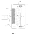
- Fig. 3 shows a general schematic as a cross-sectional view of an exemplary DC sputtering chamber 60 according to one embodiment of the present invention.
- a DC power source 62 is configured to control and supply DC power to the chamber 60.
- the DC power source applies a voltage to the cathode 64 to create a voltage potential between the cathode 64 and an anode formed by the chamber wall, such that the substrate is in between the cathode and anode.
- the glass substrate 12 is held between top support 66 and bottom support 67 via wires 68 and 69, respectively.
- the glass substrate is positioned within the sputtering chamber 60 such that the TCO layer 14 is formed on the surface facing the cathode 64.
- a plasma field 70 is created once the sputtering atmosphere is ignited, and is sustained in response to the voltage potential between the cathode 64 and the chamber wall acting as an anode.
- the voltage potential causes the plasma ions within the plasma field 70 to accelerate toward the cathode 64, causing atoms from the cathode 64 to be ejected toward the surface on the glass substrate 12.
- the cathode 64 can be referred to as a "target" and acts as the source material for the formation of the TCO layer 14 on the surface facing the cathode 64.
- the cathode 64 can be a metal alloy target, such as elemental tin, elemental zinc, or mixtures thereof. Additionally, in some embodiments, a plurality of cathodes 64 can be utilized.
- a plurality of cathodes 64 can be particularly useful to form a layer including several types of materials (e.g., co-sputtering). Since the sputtering atmosphere contains oxygen gas, oxygen particles of the plasma field 70 can react with the ejected target atoms to form an oxide layer on the TCO layer 14 on the glass substrate 12.
- materials e.g., co-sputtering. Since the sputtering atmosphere contains oxygen gas, oxygen particles of the plasma field 70 can react with the ejected target atoms to form an oxide layer on the TCO layer 14 on the glass substrate 12.
- the voltage potential can be realized through the use of multiple power sources coupled together.
- the exemplary sputtering chamber 60 is shown having a vertical orientation, although any other configuration can be utilized.
- the TCO layer can be formed via sputtering at the specified sputtering temperature from a cadmium stannate target to form a cadmium stannate TCO layer on the substrate.
- the presently provided methods of sputtering a TCO layer can be utilized in the formation of any film stack that utilizes a TCO layer, particularly those including a cadmium stannate TCO layer.
- the TCO layer can be used during the formation of any cadmium telluride device that utilizes a cadmium telluride layer, such as in the cadmium telluride thin film photovoltaic device disclosed in U.S. Publication No. 2009/0194165 of Murphy, et al. titled "Ultra-high Current Density Cadmium Telluride Photovoltaic Modules.”
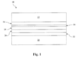
- Fig. 1 represents an exemplary cadmium telluride thin film photovoltaic device 10 that can be formed according to methods described herein.
- the exemplary device 10 of Fig. 1 includes a top sheet of glass 12 employed as the substrate.
- the glass 12 can be referred to as a "superstrate,” as it is the substrate on which the subsequent layers are formed even though it faces upward to the radiation source (e.g., the sun) when the cadmium telluride thin film photovoltaic device 10 is in use.
- the top sheet of glass 12 can be a high-transmission glass (e.g., high transmission borosilicate glass), low-iron float glass, or other highly transparent glass material.
- the glass is generally thick enough to provide support for the subsequent film layers (e.g., from about 0.5 mm to about 10 mm thick), and is substantially flat to provide a good surface for forming the subsequent film layers.
- the glass 12 can be a low iron float glass containing less than about 0.015% by weight iron (Fe), and may have a transmissiveness of about 0.9 or greater in the spectrum of interest (e.g., wavelengths from about 300 nm to about 900 nm).
- borosilicate glass may be utilized so as to better withstand high temperature processing.
- the transparent conductive oxide (TCO) layer 14 is shown on the glass 12 of the exemplary device 10 of Fig. 1 .
- the TCO layer 14 allows light to pass through with minimal absorption while also allowing electric current produced by the device 10 to travel sideways to opaque metal conductors (not shown).
- the TCO layer 14 can have a sheet resistance less than about 30 ohm per square, such as from about 4 ohm per square to about 20 ohm per square (e.g., from about 8 ohm per square to about 15 ohm per square).
- the TCO layer 14 can have a thickness between about 0.1 ⁇ m and about 1 ⁇ m, for example from about 0.1 ⁇ m to about 0.5 ⁇ m, such as from about 0.25 ⁇ m to about 0.35 ⁇ m.
- a resistive transparent buffer layer 16 (RTB layer) is shown on the TCO layer 14 on the exemplary cadmium telluride thin film photovoltaic device 10.
- the RTB layer 16 is generally more resistive than the TCO layer 14 and can help protect the device 10 from chemical interactions between the TCO layer 14 and the subsequent layers during processing of the device 10.
- the RTB layer 16 can have a sheet resistance that is greater than about 1000 ohms per square, such as from about 10 kOhms per square to about 1000 MOhms per square.
- the RTB layer 16 can also have a wide optical bandgap (e.g., greater than about 2.5 eV, such as from about 2.7 eV to about 3.0 eV).
- the presence of the RTB layer 16 between the TCO layer 14 and the cadmium sulfide layer 18 can allow for a relatively thin cadmium sulfide layer 18 to be included in the device 10 by reducing the possibility of interface defects (i.e., "pinholes" in the cadmium sulfide layer 18) creating shunts between the TCO layer 14 and the cadmium telluride layer 22.
- the RTB layer 16 allows for improved adhesion and/or interaction between the TCO layer 14 and the cadmium telluride layer 22, thereby allowing a relatively thin cadmium sulfide layer 18 to be formed thereon without significant adverse effects that would otherwise result from such a relatively thin cadmium sulfide layer 18 formed directly on the TCO layer 14.
- the RTB layer 16 can include, for instance, a combination of zinc oxide (ZnO) and tin oxide (SnO 2 ) which can be referred to as a zinc tin oxide layer ("ZTO").
- ZTO zinc tin oxide layer
- the RTB layer 16 can include more tin oxide than zinc oxide.
- the RTB layer 16 can have a composition with a stoichiometric ratio of ZnO/SnO 2 between about 0.25 and about 3, such as in about an one to two (1:2) stoichiometric ratio of tin oxide to zinc oxide.
- the RTB layer 16 can be formed by sputtering, chemical vapor deposition, spraying pryolysis, or any other suitable deposition method.
- the RTB layer 16 can be formed by sputtering (e.g. DC sputtering or RF sputtering) on the TCO layer 14 (as discussed below in greater detail with respect to the deposition of the cadmium sulfide layer 18).
- the RTB layer 16 can be deposited using a DC sputtering method by applying a DC current to a metallic source material (e.g., elemental zinc, elemental tin, or a mixture thereof) and sputtering the metallic source material onto the TCO layer 14 in the presence of an oxidizing atmosphere (e.g., O 2 gas).
- the oxidizing atmosphere includes oxygen gas (i.e., O 2 )
- the atmosphere can be greater than about 95% pure oxygen, such as greater than about 99%.
- the RTB layer 16 can have a thickness between about 0.075 ⁇ m and about 1 ⁇ m, for example from about 0.1 ⁇ m to about 0.5 ⁇ m. In particular embodiments, the RTB layer 16 can have a thickness between about 0.08 ⁇ m and about 0.2 ⁇ m, for example from about 0.1 ⁇ m to about 0.15 ⁇ m.
- a cadmium sulfide layer 18 is shown on RTB layer 16 of the exemplary device 10 of Fig. 1 .
- the cadmium sulfide layer 18 is a n-type layer that generally includes cadmium sulfide (CdS) but may also include other materials, such as zinc sulfide, cadmium zinc sulfide, etc., and mixtures thereof as well as dopants and other impurities.
- the cadmium sulfide layer may include oxygen up to about 25% by atomic percentage, for example from about 5% to about 20% by atomic percentage.
- the cadmium sulfide layer 18 can have a wide band gap (e.g., from about 2.25 eV to about 2.5 eV, such as about 2.4 eV) in order to allow most radiation energy (e.g., solar radiation) to pass. As such, the cadmium sulfide layer 18 is considered a transparent layer on the device 10.
- the cadmium sulfide layer 18 can be formed by sputtering, chemical vapor deposition, chemical bath deposition, and other suitable deposition methods.
- the cadmium sulfide layer 18 can be formed by sputtering (e.g., direct current (DC) sputtering or radio frequency (RF) sputtering) on the resistive transparent layer 16.
- Sputtering deposition generally involves ejecting material from a target, which is the material source, and depositing the ejected material onto the substrate to form the film.
- DC sputtering generally involves applying a voltage to a metal target (i.e., the cathode) positioned near the substrate (i.e., the anode) within a sputtering chamber to form a direct-current discharge.
- the sputtering chamber can have a reactive atmosphere (e.g., an oxygen atmosphere, nitrogen atmosphere, fluorine atmosphere) that forms a plasma field between the metal target and the substrate.
- the pressure of the reactive atmosphere can be between about 1 mTorr and about 20 mTorr for magnetron sputtering.
- RF sputtering generally involves exciting a capacitive discharge by applying an alternating-current (AC) or radio-frequency (RF) signal between the target (e.g., a ceramic source material) and the substrate.
- the sputtering chamber can have an inert atmosphere (e.g., an argon atmosphere) having a pressure between about 1 mTorr and about 20 mTorr.
- the cadmium sulfide layer 18 can have a thickness that is less than about 0.1 ⁇ m, such as between about 10 nm and about 100 nm, such as from about 50 nm to about 80 ⁇ m, with a minimal presence of pinholes between the resistive transparent layer 16 and the cadmium sulfide layer 18. Additionally, a cadmium sulfide layer 18 having a thickness less than about 0.1 ⁇ m reduces any absorption of radiation energy by the cadmium sulfide layer 18, effectively increasing the amount of radiation energy reaching the underlying cadmium telluride layer 22.
- a cadmium telluride layer 20 is shown on the cadmium sulfide layer 18 in the exemplary cadmium telluride thin film photovoltaic device 10 of Fig. 1 .
- the cadmium telluride layer 20 is a p-type layer that generally includes cadmium telluride (CdTe) but may also include other materials.
- the cadmium telluride layer 20 is the photovoltaic layer that interacts with the cadmium sulfide layer 18 (i.e., the n-type layer) to produce current from the absorption of radiation energy by absorbing the majority of the radiation energy passing into the device 10 due to its high absorption coefficient and creating electron-hole pairs.
- the cadmium telluride layer 20 can generally be formed from cadmium telluride and can have a bandgap tailored to absorb radiation energy (e.g., from about 1.4 eV to about 1.5 eV, such as about 1.45 eV) to create the maximum number of electron-hole pairs with the highest electrical potential (voltage) upon absorption of the radiation energy. Electrons may travel from the p-type side (i.e., the cadmium telluride layer 20) across the junction to the n-type side (i.e., the cadmium sulfide layer 18) and, conversely, holes may pass from the n-type side to the p-type side.
- radiation energy e.g., from about 1.4 eV to about 1.5 eV, such as about 1.45 eV
- Electrons may travel from the p-type side (i.e., the cadmium telluride layer 20) across the junction to the n-type side (i.e., the
- the p-n junction formed between the cadmium sulfide layer 18 and the cadmium telluride layer 20 forms a diode in which the charge imbalance leads to the creation of an electric field spanning the p-n junction.
- Conventional current is allowed to flow in only one direction and separates the light induced electron-hole pairs.
- the cadmium telluride layer 20 can be formed by any known process, such as vapor transport deposition, chemical vapor deposition (CVD), spray pyrolysis, electrodeposition, sputtering, close-space sublimation (CSS), etc.
- the cadmium sulfide layer 18 is deposited by a sputtering and the cadmium telluride layer 20 is deposited by close-space sublimation.
- the cadmium telluride layer 20 can have a thickness between about 0.1 ⁇ m and about 10 ⁇ m, such as from about 1 ⁇ m and about 5 ⁇ m.
- the cadmium telluride layer 20 can have a thickness between about 2 ⁇ m and about 4 ⁇ m, such as about 3 ⁇ m.
- a series of post-forming treatments can be applied to the exposed surface of the cadmium telluride layer 20. These treatments can tailor the functionality of the cadmium telluride layer 20 and prepare its surface for subsequent adhesion to the back contact layer(s) 22.
- the cadmium telluride layer 20 can be annealed at elevated temperatures (e.g., from about 350° C to about 500° C, such as from about 375° C to about 424° C) for a sufficient time (e.g., from about 1 to about 10 minutes) to create a quality p-type layer of cadmium telluride.
- annealing the cadmium telluride layer 20 converts the normally lightly p-type doped, or even n-type doped cadmium telluride layer 20 to a more strongly p-type cadmium telluride layer 20 having a relatively low resistivity. Additionally, the cadmium telluride layer 20 can recrystallize and undergo grain growth during annealing.
- Annealing the cadmium telluride layer 20 can be carried out in the presence of cadmium chloride in order to dope the cadmium telluride layer 20 with chloride ions.
- the cadmium telluride layer 20 can be washed with an aqueous solution containing cadmium chloride and then annealed at the elevated temperature.
- the surface after annealing the cadmium telluride layer 20 in the presence of cadmium chloride, the surface can be washed to remove any cadmium oxide formed on the surface.
- This surface preparation can leave a Te-rich surface on the cadmium telluride layer 20 by removing oxides from the surface, such as CdO, CdTeO 3 , CdTe 2 O 5 , etc.
- the surface can be washed with a suitable solvent (e.g., ethylenediamine also known as 1,2 diaminoethane or "DAE") to remove any cadmium oxide from the surface.
- a suitable solvent e.g., ethylenediamine also known as 1,2 diaminoethane or "DAE
- copper can be added to the cadmium telluride layer 20.
- the addition of copper to the cadmium telluride layer 20 can form a surface of copper-telluride on the cadmium telluride layer 20 in order to obtain a low-resistance electrical contact between the cadmium telluride layer 20 (i.e., the p-type layer) and the back contact layer(s).
- the addition of copper can create a surface layer of cuprous telluride (Cu 2 Te) between the cadmium telluride layer 20 and the back contact layer 22.
- the Te-rich surface of the cadmium telluride layer 20 can enhance the collection of current created by the device through lower resistivity between the cadmium telluride layer 20 and the back contact layer 22.
- Copper can be applied to the exposed surface of the cadmium telluride layer 20 by any process.
- copper can be sprayed or washed on the surface of the cadmium telluride layer 20 in a solution with a suitable solvent (e.g., methanol, water, or the like, or combinations thereof) followed by annealing.
- the copper may be supplied in the solution in the form of copper chloride, copper iodide, or copper acetate.
- the annealing temperature is sufficient to allow diffusion of the copper ions into the cadmium telluride layer 20, such as from about 125° C to about 300° C (e.g. from about 150° C to about 200° C) for about 5 minutes to about 30 minutes, such as from about 10 to about 25 minutes.
- a back contact layer 22 is shown on the cadmium telluride layer 20.
- the back contact layer 22 generally serves as the back electrical contact, in relation to the opposite, TCO layer 14 serving as the front electrical contact.
- the back contact layer 22 can be formed on, and in one embodiment is in direct contact with, the cadmium telluride layer 20.
- the back contact layer 22 is suitably made from one or more highly conductive materials, such as elemental nickel, chromium, copper, tin, aluminum, gold, silver, technetium or alloys or mixtures thereof. Additionally, the back contact layer 22 can be a single layer or can be a plurality of layers.
- the back contact layer 22 can include graphite, such as a layer of carbon deposited on the p-layer followed by one or more layers of metal, such as the metals described above.
- the back contact layer 22, if made of or comprising one or more metals, is suitably applied by a technique such as sputtering or metal evaporation. If it is made from a graphite and polymer blend, or from a carbon paste, the blend or paste is applied to the semiconductor device by any suitable method for spreading the blend or paste, such as screen printing, spraying or by a "doctor" blade. After the application of the graphite blend or carbon paste, the device can be heated to convert the blend or paste into the conductive back contact layer.
- a carbon layer if used, can be from about 0.1 ⁇ m to about 10 ⁇ m in thickness, for example from about 1 ⁇ m to about 5 ⁇ m.
- a metal layer of the back contact if used for or as part of the back contact layer 22, can be from about 0.1 ⁇ m to about 1.5 ⁇ m in thickness.
- the encapsulating glass 24 is also shown in the exemplary cadmium telluride thin film photovoltaic device 10 of Fig. 1 .
- exemplary device 10 can include bus bars, external wiring, laser etches, etc.
- a plurality of photovoltaic cells can be connected in series in order to achieve a desired voltage, such as through an electrical wiring connection.
- Each end of the series connected cells can be attached to a suitable conductor such as a wire or bus bar, to direct the photovoltaically generated current to convenient locations for connection to a device or other system using the generated electric.
- a convenient means for achieving such series connections is to laser scribe the device to divide the device into a series of cells connected by interconnects.
- a laser can be used to scribe the deposited layers of the semiconductor device to divide the device into a plurality of series connected cells.
- Fig. 2 shows a flow diagram of an exemplary method 30 of manufacturing a photovoltaic device according to one embodiment of the present invention.
- a TCO layer is formed on a glass substrate at 32.
- a resistive transparent layer is formed on the TCO layer.
- a cadmium sulfide layer is formed on the resistive transparent layer at 36, and a cadmium telluride layer is formed on the cadmium sulfide layer at 38.
- the cadmium telluride layer can be annealed in the presence of cadmium chloride at 40, and washed to remove any oxides formed on the surface at 42.
- the cadmium telluride layer can be doped with copper at 44.
- back contact layer(s) can be applied over the cadmium telluride layer, and an encapsulating glass can be applied over the back contact layer at 48.
- the method may also include laser scribing to form electrically isolated photovoltaic cells in the device. These electrically isolated photovoltaic cells can then be connected in series to form a photovoltaic module. Also, electrical wires can be connected to positive and negative terminals of the photovoltaic module to provide lead wires to harness electrical current produced by the photovoltaic module.
Landscapes
- Chemical & Material Sciences (AREA)
- Chemical Kinetics & Catalysis (AREA)
- Engineering & Computer Science (AREA)
- Materials Engineering (AREA)
- Mechanical Engineering (AREA)
- Metallurgy (AREA)
- Organic Chemistry (AREA)
- Photovoltaic Devices (AREA)
- Physical Vapour Deposition (AREA)
Applications Claiming Priority (1)
| Application Number | Priority Date | Filing Date | Title |
|---|---|---|---|
| US12/750,116 US8043954B1 (en) | 2010-03-30 | 2010-03-30 | Methods of forming a conductive transparent oxide film layer for use in a cadmium telluride based thin film photovoltaic device |
Publications (2)
| Publication Number | Publication Date |
|---|---|
| EP2371990A1 true EP2371990A1 (de) | 2011-10-05 |
| EP2371990B1 EP2371990B1 (de) | 2015-10-21 |
Family
ID=44080294
Family Applications (1)
| Application Number | Title | Priority Date | Filing Date |
|---|---|---|---|
| EP11160307.2A Not-in-force EP2371990B1 (de) | 2010-03-30 | 2011-03-29 | Verfahren zur Bildung einer leitfähigen transparenten Oxidfolienschicht zur Verwendung in einer Cadmiumtellurid-basierten Dünnschichtphotovoltaikvorrichtung |
Country Status (4)
| Country | Link |
|---|---|
| US (1) | US8043954B1 (de) |
| EP (1) | EP2371990B1 (de) |
| CN (1) | CN102208484B (de) |
| AU (1) | AU2011201273B2 (de) |
Families Citing this family (5)
| Publication number | Priority date | Publication date | Assignee | Title |
|---|---|---|---|---|
| US8252618B2 (en) * | 2009-12-15 | 2012-08-28 | Primestar Solar, Inc. | Methods of manufacturing cadmium telluride thin film photovoltaic devices |
| WO2012083018A1 (en) * | 2010-12-17 | 2012-06-21 | First Solar, Inc. | Photovoltaic device |
| CN104425653B (zh) * | 2013-08-30 | 2017-11-21 | 中国建材国际工程集团有限公司 | 用于薄层太阳能电池的附加的底层 |
| DE102014225862B4 (de) * | 2014-12-15 | 2023-01-19 | China Triumph International Engineering Co., Ltd. | Verfahren zur Bildung einer Dünnschicht mit Gradient mittels Spraypyrolyse |
| CN112582483A (zh) * | 2019-09-30 | 2021-03-30 | 康宁股份有限公司 | 具有强化的近红外性质的透明导体材料及其形成方法 |
Citations (2)
| Publication number | Priority date | Publication date | Assignee | Title |
|---|---|---|---|---|
| US5922142A (en) * | 1996-11-07 | 1999-07-13 | Midwest Research Institute | Photovoltaic devices comprising cadmium stannate transparent conducting films and method for making |
| US20090194165A1 (en) | 2008-01-31 | 2009-08-06 | Primestar Solar, Inc. | Ultra-high current density cadmium telluride photovoltaic modules |
Family Cites Families (21)
| Publication number | Priority date | Publication date | Assignee | Title |
|---|---|---|---|---|
| US3811953A (en) | 1971-09-20 | 1974-05-21 | American Cyanamid Co | Light-transmitting electrically conducting cadmium stannate and methods of producing same |
| DE3168017D1 (en) | 1980-05-27 | 1985-02-14 | Secr Defence Brit | Manufacture of cadmium mercury telluride |
| US4439267A (en) | 1982-09-29 | 1984-03-27 | The United States Of America As Represented By The Secretary Of The Army | Vapor-phase method for growing mercury cadmium telluride |
| GB2185256B (en) | 1985-04-09 | 1988-04-07 | Secr Defence | Preparation of group ii metal alkyls |
| US5123995A (en) | 1990-10-04 | 1992-06-23 | Aerodyne Research, Inc. | Low-temperature, photo-induced epitaxy |
| DE4132882C2 (de) | 1991-10-03 | 1996-05-09 | Antec Angewandte Neue Technolo | Verfahren zur Herstellung von pn CdTe/CdS-Dünnschichtsolarzellen |
| US5261968A (en) | 1992-01-13 | 1993-11-16 | Photon Energy, Inc. | Photovoltaic cell and method |
| US6221495B1 (en) | 1996-11-07 | 2001-04-24 | Midwest Research Institute | Thin transparent conducting films of cadmium stannate |
| US6169246B1 (en) | 1998-09-08 | 2001-01-02 | Midwest Research Institute | Photovoltaic devices comprising zinc stannate buffer layer and method for making |
| US6137048A (en) | 1996-11-07 | 2000-10-24 | Midwest Research Institute | Process for fabricating polycrystalline semiconductor thin-film solar cells, and cells produced thereby |
| US6517687B1 (en) | 1999-03-17 | 2003-02-11 | General Electric Company | Ultraviolet filters with enhanced weatherability and method of making |
| US6420032B1 (en) | 1999-03-17 | 2002-07-16 | General Electric Company | Adhesion layer for metal oxide UV filters |
| US6365016B1 (en) | 1999-03-17 | 2002-04-02 | General Electric Company | Method and apparatus for arc plasma deposition with evaporation of reagents |
| US6426125B1 (en) | 1999-03-17 | 2002-07-30 | General Electric Company | Multilayer article and method of making by ARC plasma deposition |
| US6261694B1 (en) | 1999-03-17 | 2001-07-17 | General Electric Company | Infrared reflecting coatings |
| WO2002091483A2 (en) | 2001-05-08 | 2002-11-14 | Bp Corporation North America Inc. | Improved photovoltaic device |
| WO2003052837A1 (en) | 2001-12-13 | 2003-06-26 | Midwest Research Institute | Semiconductor device with higher oxygen (o2) concentration within window layers and method for making |
| US7601558B2 (en) | 2006-10-24 | 2009-10-13 | Applied Materials, Inc. | Transparent zinc oxide electrode having a graded oxygen content |
| JP2010512664A (ja) | 2006-12-11 | 2010-04-22 | ルーメンツ リミテッド ライアビリティ カンパニー | 酸化亜鉛多接合光電池及び光電子装置 |
| JP5291928B2 (ja) | 2007-12-26 | 2013-09-18 | 株式会社日立製作所 | 酸化物半導体装置およびその製造方法 |
| CA2722572A1 (en) | 2008-05-01 | 2009-11-05 | First Solar, Inc. | Transparent conductive materials including cadmium stannate |
-
2010
- 2010-03-30 US US12/750,116 patent/US8043954B1/en not_active Expired - Fee Related
-
2011
- 2011-03-22 AU AU2011201273A patent/AU2011201273B2/en not_active Ceased
- 2011-03-29 EP EP11160307.2A patent/EP2371990B1/de not_active Not-in-force
- 2011-03-30 CN CN201110089632.6A patent/CN102208484B/zh not_active Expired - Fee Related
Patent Citations (2)
| Publication number | Priority date | Publication date | Assignee | Title |
|---|---|---|---|---|
| US5922142A (en) * | 1996-11-07 | 1999-07-13 | Midwest Research Institute | Photovoltaic devices comprising cadmium stannate transparent conducting films and method for making |
| US20090194165A1 (en) | 2008-01-31 | 2009-08-06 | Primestar Solar, Inc. | Ultra-high current density cadmium telluride photovoltaic modules |
Non-Patent Citations (2)
| Title |
|---|
| HAACKE G ET AL: "Sputter deposition and characterization of Cd2SnO4 films", THIN SOLID FILMS, ELSEVIER-SEQUOIA S.A. LAUSANNE, CH, vol. 55, no. 1, 15 November 1978 (1978-11-15), pages 67 - 81, XP025698583, ISSN: 0040-6090, [retrieved on 19781115], DOI: 10.1016/0040-6090(78)90075-5 * |
| ROMEO N ET AL: "Comparison of different conducting oxides as substrates for CdS/CdTe thin film solar cells", THIN SOLID FILMS, ELSEVIER-SEQUOIA S.A. LAUSANNE, CH, vol. 431-432, 1 May 2003 (2003-05-01), pages 364 - 368, XP004428668, ISSN: 0040-6090, DOI: 10.1016/S0040-6090(03)00239-6 * |
Also Published As
| Publication number | Publication date |
|---|---|
| CN102208484A (zh) | 2011-10-05 |
| AU2011201273B2 (en) | 2012-07-05 |
| CN102208484B (zh) | 2016-09-21 |
| US8043954B1 (en) | 2011-10-25 |
| US20110244621A1 (en) | 2011-10-06 |
| AU2011201273A1 (en) | 2011-10-20 |
| EP2371990B1 (de) | 2015-10-21 |
Similar Documents
| Publication | Publication Date | Title |
|---|---|---|
| US8143515B2 (en) | Cadmium telluride thin film photovoltaic devices and methods of manufacturing the same | |
| US8043955B1 (en) | Methods of forming a conductive transparent oxide film layer for use in a cadmium telluride based thin film photovoltaic device | |
| US8252618B2 (en) | Methods of manufacturing cadmium telluride thin film photovoltaic devices | |
| EP2337084A2 (de) | Telluridschicht mit abgestufter Legierung in Cadmiumtellurid-Dünnfilmfotovoltaikvorrichtungen und Herstellungsverfahren dafür | |
| US8257561B2 (en) | Methods of forming a conductive transparent oxide film layer for use in a cadmium telluride based thin film photovoltaic device | |
| US8247683B2 (en) | Thin film interlayer in cadmium telluride thin film photovoltaic devices and methods of manufacturing the same | |
| US8053350B2 (en) | Methods of forming a conductive transparent oxide film layer for use in a cadmium telluride based thin film photovoltaic device | |
| EP2383363A1 (de) | Cadmiumsulfidschichten zur Verwendung in Cadmiumtellurid-basierten Dünnfilmfotovoltaikvorrichtungen und Herstellungsverfahren dafür | |
| EP2383792A2 (de) | Cadmiumsulfidschichten zur Verwendung in Cadmiumtellurid-basierten Dünnfilmfotovoltaikvorrichtungen und Herstellungsverfahren dafür | |
| EP2371990B1 (de) | Verfahren zur Bildung einer leitfähigen transparenten Oxidfolienschicht zur Verwendung in einer Cadmiumtellurid-basierten Dünnschichtphotovoltaikvorrichtung | |
| EP2383362A1 (de) | Vorrichtungen und Verfahren zum Schutz von einer Cadmiumsulfidschicht zur Weiterverarbeitung | |
| EP2403016B1 (de) | Verfahren zur Bildung einer leitfähigen transparenten Oxidfolienschicht zur Verwendung in einer Cadmiumtellurid-basierten Dünnschichtphotovoltaikvorrichtung | |
| US8236601B2 (en) | Apparatus and methods of forming a conductive transparent oxide film layer for use in a cadmium telluride based thin film photovoltaic device | |
| US20120052621A1 (en) | Methods of forming a window layer in a cadmium telluride based thin film photovoltaic device | |
| EP2402479B1 (de) | Verfahren zum Aufdampfen eines resistiven transparenten Dünnfilms zur Verwendung in Cadmiumtellurid-basierten Photovoltaikvorrichtungen | |
| US20130133731A1 (en) | Cadmium doped tin oxide buffer layer for thin film photovoltaic devices and their methods of manufacture | |
| US20120024692A1 (en) | Mixed sputtering targets and their use in cadmium sulfide layers of cadmium telluride vased thin film photovoltaic devices | |
| US20130134037A1 (en) | Mixed targets for forming a cadmium doped tin oxide buffer layer in a thin film photovoltaic devices |
Legal Events
| Date | Code | Title | Description |
|---|---|---|---|
| PUAI | Public reference made under article 153(3) epc to a published international application that has entered the european phase |
Free format text: ORIGINAL CODE: 0009012 |
|
| AK | Designated contracting states |
Kind code of ref document: A1 Designated state(s): AL AT BE BG CH CY CZ DE DK EE ES FI FR GB GR HR HU IE IS IT LI LT LU LV MC MK MT NL NO PL PT RO RS SE SI SK SM TR |
|
| AX | Request for extension of the european patent |
Extension state: BA ME |
|
| 17P | Request for examination filed |
Effective date: 20120405 |
|
| RAP1 | Party data changed (applicant data changed or rights of an application transferred) |
Owner name: FIRST SOLAR MALAYSIA SDN.BHD |
|
| GRAP | Despatch of communication of intention to grant a patent |
Free format text: ORIGINAL CODE: EPIDOSNIGR1 |
|
| INTG | Intention to grant announced |
Effective date: 20150513 |
|
| GRAS | Grant fee paid |
Free format text: ORIGINAL CODE: EPIDOSNIGR3 |
|
| GRAA | (expected) grant |
Free format text: ORIGINAL CODE: 0009210 |
|
| AK | Designated contracting states |
Kind code of ref document: B1 Designated state(s): AL AT BE BG CH CY CZ DE DK EE ES FI FR GB GR HR HU IE IS IT LI LT LU LV MC MK MT NL NO PL PT RO RS SE SI SK SM TR |
|
| REG | Reference to a national code |
Ref country code: GB Ref legal event code: FG4D Ref country code: NL Ref legal event code: MP Effective date: 20151021 |
|
| REG | Reference to a national code |
Ref country code: CH Ref legal event code: EP |
|
| REG | Reference to a national code |
Ref country code: AT Ref legal event code: REF Ref document number: 756666 Country of ref document: AT Kind code of ref document: T Effective date: 20151115 |
|
| REG | Reference to a national code |
Ref country code: IE Ref legal event code: FG4D |
|
| REG | Reference to a national code |
Ref country code: DE Ref legal event code: R096 Ref document number: 602011020723 Country of ref document: DE |
|
| REG | Reference to a national code |
Ref country code: LT Ref legal event code: MG4D |
|
| REG | Reference to a national code |
Ref country code: AT Ref legal event code: MK05 Ref document number: 756666 Country of ref document: AT Kind code of ref document: T Effective date: 20151021 |
|
| PG25 | Lapsed in a contracting state [announced via postgrant information from national office to epo] |
Ref country code: NL Free format text: LAPSE BECAUSE OF FAILURE TO SUBMIT A TRANSLATION OF THE DESCRIPTION OR TO PAY THE FEE WITHIN THE PRESCRIBED TIME-LIMIT Effective date: 20151021 Ref country code: HR Free format text: LAPSE BECAUSE OF FAILURE TO SUBMIT A TRANSLATION OF THE DESCRIPTION OR TO PAY THE FEE WITHIN THE PRESCRIBED TIME-LIMIT Effective date: 20151021 Ref country code: LT Free format text: LAPSE BECAUSE OF FAILURE TO SUBMIT A TRANSLATION OF THE DESCRIPTION OR TO PAY THE FEE WITHIN THE PRESCRIBED TIME-LIMIT Effective date: 20151021 Ref country code: ES Free format text: LAPSE BECAUSE OF FAILURE TO SUBMIT A TRANSLATION OF THE DESCRIPTION OR TO PAY THE FEE WITHIN THE PRESCRIBED TIME-LIMIT Effective date: 20151021 Ref country code: IT Free format text: LAPSE BECAUSE OF FAILURE TO SUBMIT A TRANSLATION OF THE DESCRIPTION OR TO PAY THE FEE WITHIN THE PRESCRIBED TIME-LIMIT Effective date: 20151021 Ref country code: IS Free format text: LAPSE BECAUSE OF FAILURE TO SUBMIT A TRANSLATION OF THE DESCRIPTION OR TO PAY THE FEE WITHIN THE PRESCRIBED TIME-LIMIT Effective date: 20160221 Ref country code: NO Free format text: LAPSE BECAUSE OF FAILURE TO SUBMIT A TRANSLATION OF THE DESCRIPTION OR TO PAY THE FEE WITHIN THE PRESCRIBED TIME-LIMIT Effective date: 20160121 |
|
| PG25 | Lapsed in a contracting state [announced via postgrant information from national office to epo] |
Ref country code: PL Free format text: LAPSE BECAUSE OF FAILURE TO SUBMIT A TRANSLATION OF THE DESCRIPTION OR TO PAY THE FEE WITHIN THE PRESCRIBED TIME-LIMIT Effective date: 20151021 Ref country code: RS Free format text: LAPSE BECAUSE OF FAILURE TO SUBMIT A TRANSLATION OF THE DESCRIPTION OR TO PAY THE FEE WITHIN THE PRESCRIBED TIME-LIMIT Effective date: 20151021 Ref country code: GR Free format text: LAPSE BECAUSE OF FAILURE TO SUBMIT A TRANSLATION OF THE DESCRIPTION OR TO PAY THE FEE WITHIN THE PRESCRIBED TIME-LIMIT Effective date: 20160122 Ref country code: SE Free format text: LAPSE BECAUSE OF FAILURE TO SUBMIT A TRANSLATION OF THE DESCRIPTION OR TO PAY THE FEE WITHIN THE PRESCRIBED TIME-LIMIT Effective date: 20151021 Ref country code: LV Free format text: LAPSE BECAUSE OF FAILURE TO SUBMIT A TRANSLATION OF THE DESCRIPTION OR TO PAY THE FEE WITHIN THE PRESCRIBED TIME-LIMIT Effective date: 20151021 Ref country code: PT Free format text: LAPSE BECAUSE OF FAILURE TO SUBMIT A TRANSLATION OF THE DESCRIPTION OR TO PAY THE FEE WITHIN THE PRESCRIBED TIME-LIMIT Effective date: 20160222 Ref country code: FI Free format text: LAPSE BECAUSE OF FAILURE TO SUBMIT A TRANSLATION OF THE DESCRIPTION OR TO PAY THE FEE WITHIN THE PRESCRIBED TIME-LIMIT Effective date: 20151021 Ref country code: AT Free format text: LAPSE BECAUSE OF FAILURE TO SUBMIT A TRANSLATION OF THE DESCRIPTION OR TO PAY THE FEE WITHIN THE PRESCRIBED TIME-LIMIT Effective date: 20151021 |
|
| REG | Reference to a national code |
Ref country code: DE Ref legal event code: R097 Ref document number: 602011020723 Country of ref document: DE |
|
| PG25 | Lapsed in a contracting state [announced via postgrant information from national office to epo] |
Ref country code: CZ Free format text: LAPSE BECAUSE OF FAILURE TO SUBMIT A TRANSLATION OF THE DESCRIPTION OR TO PAY THE FEE WITHIN THE PRESCRIBED TIME-LIMIT Effective date: 20151021 |
|
| PLBE | No opposition filed within time limit |
Free format text: ORIGINAL CODE: 0009261 |
|
| STAA | Information on the status of an ep patent application or granted ep patent |
Free format text: STATUS: NO OPPOSITION FILED WITHIN TIME LIMIT |
|
| PG25 | Lapsed in a contracting state [announced via postgrant information from national office to epo] |
Ref country code: SM Free format text: LAPSE BECAUSE OF FAILURE TO SUBMIT A TRANSLATION OF THE DESCRIPTION OR TO PAY THE FEE WITHIN THE PRESCRIBED TIME-LIMIT Effective date: 20151021 Ref country code: SK Free format text: LAPSE BECAUSE OF FAILURE TO SUBMIT A TRANSLATION OF THE DESCRIPTION OR TO PAY THE FEE WITHIN THE PRESCRIBED TIME-LIMIT Effective date: 20151021 Ref country code: RO Free format text: LAPSE BECAUSE OF FAILURE TO SUBMIT A TRANSLATION OF THE DESCRIPTION OR TO PAY THE FEE WITHIN THE PRESCRIBED TIME-LIMIT Effective date: 20151021 Ref country code: BE Free format text: LAPSE BECAUSE OF NON-PAYMENT OF DUE FEES Effective date: 20160331 Ref country code: DK Free format text: LAPSE BECAUSE OF FAILURE TO SUBMIT A TRANSLATION OF THE DESCRIPTION OR TO PAY THE FEE WITHIN THE PRESCRIBED TIME-LIMIT Effective date: 20151021 Ref country code: EE Free format text: LAPSE BECAUSE OF FAILURE TO SUBMIT A TRANSLATION OF THE DESCRIPTION OR TO PAY THE FEE WITHIN THE PRESCRIBED TIME-LIMIT Effective date: 20151021 |
|
| 26N | No opposition filed |
Effective date: 20160722 |
|
| PG25 | Lapsed in a contracting state [announced via postgrant information from national office to epo] |
Ref country code: LU Free format text: LAPSE BECAUSE OF FAILURE TO SUBMIT A TRANSLATION OF THE DESCRIPTION OR TO PAY THE FEE WITHIN THE PRESCRIBED TIME-LIMIT Effective date: 20160329 Ref country code: MC Free format text: LAPSE BECAUSE OF FAILURE TO SUBMIT A TRANSLATION OF THE DESCRIPTION OR TO PAY THE FEE WITHIN THE PRESCRIBED TIME-LIMIT Effective date: 20151021 |
|
| REG | Reference to a national code |
Ref country code: CH Ref legal event code: PL |
|
| GBPC | Gb: european patent ceased through non-payment of renewal fee |
Effective date: 20160329 |
|
| PG25 | Lapsed in a contracting state [announced via postgrant information from national office to epo] |
Ref country code: SI Free format text: LAPSE BECAUSE OF FAILURE TO SUBMIT A TRANSLATION OF THE DESCRIPTION OR TO PAY THE FEE WITHIN THE PRESCRIBED TIME-LIMIT Effective date: 20151021 |
|
| REG | Reference to a national code |
Ref country code: IE Ref legal event code: MM4A |
|
| PG25 | Lapsed in a contracting state [announced via postgrant information from national office to epo] |
Ref country code: BE Free format text: LAPSE BECAUSE OF FAILURE TO SUBMIT A TRANSLATION OF THE DESCRIPTION OR TO PAY THE FEE WITHIN THE PRESCRIBED TIME-LIMIT Effective date: 20151021 |
|
| REG | Reference to a national code |
Ref country code: FR Ref legal event code: ST Effective date: 20161130 |
|
| PG25 | Lapsed in a contracting state [announced via postgrant information from national office to epo] |
Ref country code: FR Free format text: LAPSE BECAUSE OF NON-PAYMENT OF DUE FEES Effective date: 20160331 Ref country code: GB Free format text: LAPSE BECAUSE OF NON-PAYMENT OF DUE FEES Effective date: 20160329 Ref country code: IE Free format text: LAPSE BECAUSE OF NON-PAYMENT OF DUE FEES Effective date: 20160329 Ref country code: LI Free format text: LAPSE BECAUSE OF NON-PAYMENT OF DUE FEES Effective date: 20160331 Ref country code: CH Free format text: LAPSE BECAUSE OF NON-PAYMENT OF DUE FEES Effective date: 20160331 |
|
| PGFP | Annual fee paid to national office [announced via postgrant information from national office to epo] |
Ref country code: TR Payment date: 20170309 Year of fee payment: 7 |
|
| PGFP | Annual fee paid to national office [announced via postgrant information from national office to epo] |
Ref country code: DE Payment date: 20170329 Year of fee payment: 7 |
|
| PG25 | Lapsed in a contracting state [announced via postgrant information from national office to epo] |
Ref country code: MT Free format text: LAPSE BECAUSE OF FAILURE TO SUBMIT A TRANSLATION OF THE DESCRIPTION OR TO PAY THE FEE WITHIN THE PRESCRIBED TIME-LIMIT Effective date: 20151021 |
|
| PG25 | Lapsed in a contracting state [announced via postgrant information from national office to epo] |
Ref country code: CY Free format text: LAPSE BECAUSE OF FAILURE TO SUBMIT A TRANSLATION OF THE DESCRIPTION OR TO PAY THE FEE WITHIN THE PRESCRIBED TIME-LIMIT Effective date: 20151021 Ref country code: HU Free format text: LAPSE BECAUSE OF FAILURE TO SUBMIT A TRANSLATION OF THE DESCRIPTION OR TO PAY THE FEE WITHIN THE PRESCRIBED TIME-LIMIT; INVALID AB INITIO Effective date: 20110329 |
|
| PG25 | Lapsed in a contracting state [announced via postgrant information from national office to epo] |
Ref country code: MK Free format text: LAPSE BECAUSE OF FAILURE TO SUBMIT A TRANSLATION OF THE DESCRIPTION OR TO PAY THE FEE WITHIN THE PRESCRIBED TIME-LIMIT Effective date: 20151021 Ref country code: MT Free format text: LAPSE BECAUSE OF FAILURE TO SUBMIT A TRANSLATION OF THE DESCRIPTION OR TO PAY THE FEE WITHIN THE PRESCRIBED TIME-LIMIT Effective date: 20160331 |
|
| PG25 | Lapsed in a contracting state [announced via postgrant information from national office to epo] |
Ref country code: BG Free format text: LAPSE BECAUSE OF FAILURE TO SUBMIT A TRANSLATION OF THE DESCRIPTION OR TO PAY THE FEE WITHIN THE PRESCRIBED TIME-LIMIT Effective date: 20151021 |
|
| REG | Reference to a national code |
Ref country code: DE Ref legal event code: R119 Ref document number: 602011020723 Country of ref document: DE |
|
| PG25 | Lapsed in a contracting state [announced via postgrant information from national office to epo] |
Ref country code: AL Free format text: LAPSE BECAUSE OF FAILURE TO SUBMIT A TRANSLATION OF THE DESCRIPTION OR TO PAY THE FEE WITHIN THE PRESCRIBED TIME-LIMIT Effective date: 20151021 |
|
| PG25 | Lapsed in a contracting state [announced via postgrant information from national office to epo] |
Ref country code: DE Free format text: LAPSE BECAUSE OF NON-PAYMENT OF DUE FEES Effective date: 20181002 |
|
| PG25 | Lapsed in a contracting state [announced via postgrant information from national office to epo] |
Ref country code: TR Free format text: LAPSE BECAUSE OF NON-PAYMENT OF DUE FEES Effective date: 20180329 |