EP2372491B1 - Procédé de réglage du blocage de l'alimentation et appareil électronique l'utilisant - Google Patents
Procédé de réglage du blocage de l'alimentation et appareil électronique l'utilisant Download PDFInfo
- Publication number
- EP2372491B1 EP2372491B1 EP10164990.3A EP10164990A EP2372491B1 EP 2372491 B1 EP2372491 B1 EP 2372491B1 EP 10164990 A EP10164990 A EP 10164990A EP 2372491 B1 EP2372491 B1 EP 2372491B1
- Authority
- EP
- European Patent Office
- Prior art keywords
- power
- electronic apparatus
- operating system
- bmc
- lock
- Prior art date
- Legal status (The legal status is an assumption and is not a legal conclusion. Google has not performed a legal analysis and makes no representation as to the accuracy of the status listed.)
- Not-in-force
Links
Images




Classifications
-
- G—PHYSICS
- G06—COMPUTING OR CALCULATING; COUNTING
- G06F—ELECTRIC DIGITAL DATA PROCESSING
- G06F1/00—Details not covered by groups G06F3/00 - G06F13/00 and G06F21/00
- G06F1/26—Power supply means, e.g. regulation thereof
-
- G—PHYSICS
- G06—COMPUTING OR CALCULATING; COUNTING
- G06F—ELECTRIC DIGITAL DATA PROCESSING
- G06F11/00—Error detection; Error correction; Monitoring
- G06F11/07—Responding to the occurrence of a fault, e.g. fault tolerance
- G06F11/0703—Error or fault processing not based on redundancy, i.e. by taking additional measures to deal with the error or fault not making use of redundancy in operation, in hardware, or in data representation
- G06F11/0751—Error or fault detection not based on redundancy
- G06F11/0754—Error or fault detection not based on redundancy by exceeding limits
- G06F11/0757—Error or fault detection not based on redundancy by exceeding limits by exceeding a time limit, i.e. time-out, e.g. watchdogs
Definitions
- the invention relates to a power lock-up setting method and an electronic apparatus using the same. More particularly, the invention relates to a power lock-up setting method performed by a baseboard management controller (BMC) and an electronic apparatus using the same.
- BMC baseboard management controller
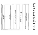
- FIG. 1 is a schematic block diagram of a server having the power button lock-up function in the related art.
- the server includes a power button 11, a general purpose input/output (GPIO) interface 12, a chipset southbridge 13, a central processing unit (CPU) 14, and a basic input/output system (BIOS) 15.
- GPIO general purpose input/output
- CPU central processing unit
- BIOS basic input/output system
- the operating system When users selects the operation mode, such as the power-off mode or the light-sleep mode, under the operating environment of the operating system, the operating system would inform the BIOS 15 to change the operation mode of the GPIO interface 12. Accordingly, when the server is in the power-off mode or the light-sleep mode, and the power button 11 is pressed again, the server is restarted.
- the operation mode such as the power-off mode or the light-sleep mode
- the users can simply force the server to be powered off by pulling out the plug thereof without powering off the server by pressing the power button 11 because the GPIO interface 12 is set to forbid the power-off mode performed by pressing the power button 11.
- the present invention is defined by the appended claims 1 and 8 providing a power lock-up setting method and an electronic apparatus using the same to solve the problem of which the users can simply force the server to be powered off by pulling out the plug thereof when the server crashes due to the error of the operating system.
- an exemplary embodiment of the invention provides a power lock-up setting method.
- the power lock-up setting method is adapted to an electronic apparatus.
- the electronic apparatus includes a power switch, a general purpose input/output (GPIO) interface, a control unit, a logic processing unit, and a processing module, wherein the logic processing unit comprises a baseboard management controller (BMC).
- the power lock-up setting method includes following steps. A trigger signal is received by a pin of the GPIO interface and transmitted to the control unit, wherein the trigger signal is generated by the power switch which is pressed. Accordingly, the control unit starts the electronic apparatus after receiving the trigger signal, and next, a power-on-self-test of the logic processing unit is performed by the processing module.
- Whether the GPIO interface is set to a power lock-up state is determined by the logic processing unit.
- a level of the pin is set to a disable level by the logic processing unit.
- An operating system is loaded by the processing module to perform an operating system booting process.
- the trigger signal is prevented from being transmitted to the control unit when being generated again.
- a power-off forcing command transmitted by the control end is received by the network connecting module, and the level of the pin is set to an enable level by the BMC according to the power-off forcing command.
- the electronic apparatus is controlled to enter a power-off mode by the BMC.
- the logic processing unit includes a basic input/output system (BIOS).
- BIOS basic input/output system
- a lock-up command is transmitted to the BMC by the BIOS such that the BMC sets the level of the pin to the disable level.
- the power lock-up setting method further includes a step of providing a network connecting module to link with a control end of a domain.
- Another exemplary embodiment of the invention provides an electronic apparatus with a corresponding power lock-up function.
- the power lock-up setting method and the electronic apparatus using the same have following advantages:
- the GPIO interface is set by the logic processing unit. Accordingly, the problem of which the power lock-up function can not be removed when the operating system hangs up.
- FIG. 1 is a schematic block diagram of a server having the power button lock-up function in the related art.
- FIG. 2 is a block diagram of an electronic apparatus with a power lock-up function according to a first embodiment of the invention.
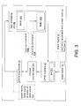
- FIG. 3 is a block diagram of an electronic apparatus with a power lock-up function according to a second embodiment of the invention.
- FIG. 4 is a block diagram of an electronic apparatus with a power lock-up function according to a third embodiment of the invention.
- FIG. 5 is a flowchart of a power lock-up setting method according to an embodiment of the invention.
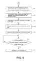
- FIG. 6 is a flowchart illustrating the continuous procedure of the power lock-up setting method in FIG. 5 according to a first embodiment of the invention.
- FIG. 7 is a flowchart illustrating the continuous procedure of the power lock-up setting method in FIG. 5 according to a second embodiment of the invention.
- FIG. 2 is a block diagram of an electronic apparatus with a power lock-up function according to a first embodiment of the invention.
- the electronic apparatus with the power lock-up function includes a power switch 21, a general purpose input/output (GPIO) interface 22, a control unit 23, a processing module 24, and a logic processing unit 25.
- GPIO general purpose input/output
- the power switch 21 When users press the power switch 21 in a touch action, the power switch 21 correspondingly generates a trigger signal 211.
- the GPIO interface 22 is connected to the power switch 21 by a pin 221 to receive the trigger signal 211 and transmit the trigger signal 211 to the control unit 23. Accordingly, the control unit 23 starts the electronic apparatus with the power lock-up function 2.
- the processing module 24 loads an operating system to perform an operating system booting process.
- POST Power-on-self-test
- the logic processing unit 25 detects a set state of the GPIO interface 22.
- the logic processing unit 25 sets a level of the pin to a disable level, such that the path between the power switch 21 and the control unit 23 becomes open-circuited. Accordingly, in the electronic apparatus with the power lock-up function 2 of the present embodiment, under an operating environment of the operating system, the trigger signal 211 generated by the power switch 21 which is carelessly touched by the users is prevented from being transmitting to the control unit 23 through the GPIO interface 22.
- a voltage value of the disable level for example, is higher than that of a predetermined conducting level.
- the control unit 23 for example, is a chipset southbridge, a chipset northbridge, or an embedded controller (EC).
- FIG. 3 is a block diagram of an electronic apparatus with a power lock-up function according to a second embodiment of the invention.
- the logic processing unit 25 of the second embodiment further includes a basic input/output system (BIOS) 251 and a baseboard management controller (BMC) 252.
- BIOS basic input/output system
- BMC baseboard management controller
- the chipset southbridge 231 substitutes for the control unit 23. The other portion is almost the same, and it will not be described again herein.
- the BIOS 251 determines whether the GPIO interface 22 is set to the power lock-up state. When determining that the GPIO interface 22 is set to the power lock-up state, the BIOS transmits a lock-up command 253 to the BMC 252, such that the BMC 252 performs an action of setting level.
- the BMC 252 also performs an embedded operating system, and the embedded operating system and the operating system performed by the processing module 24 are systems which independently operate.
- the embedded operating system for example, is a relatively stable operating system, such as Linux, so as to control the BMC 252 to collect and detect all kinds of system health information and system state information of the electronic apparatus with the power lock-up function 2. Accordingly, when serious events occur, the embedded operating system can perform a correcting action.
- the system health information for example, is the system voltage, the system temperature, and the fan speed.
- the operating system loaded by the processing module 24 is usually a system with a friendly interface for the users, such as Windows, to increase the convenience of the usage.
- the processing module transmits a power-saving mode signal or a power-off mode signal 241 to the BIOS 251. Accordingly, the BIOS 251 transmits an unlocking command 254 to the BMC 252, such that the BMC 254 sets the level of the pin 221 to an enable level, and thus, the path between the power switch 21 and the chipset southbridge 231 is connected.
- the electronic apparatus with the power lock-up function 2 of the present embodiment is in the power-saving mode or in power-off mode, the electronic apparatus 2 can be restarted by pressing the power switch 21.
- the enable level for example, is a predetermined conducting level of the pin 221.
- the power-saving mode may be an S1 state or an S4 state of an advanced configuration and power interface (ACPI), and the power-off mode is an S5 state of the ACPI.
- ACPI advanced configuration and power interface
- FIG. 4 is a block diagram of an electronic apparatus with a power lock-up function according to a third embodiment of the invention.
- the electronic apparatus with the power lock-up function 2 of the third embodiment further includes a network connecting module 26 connected to the BMC. Accordingly, a communication can be built with a control end 27 of a domain.
- the operating system may hang up due to deadlock of the operating system and application programs which is caused by unexpected events or software errors.
- the management information system personnel can transmit a power-off forcing command 271 to the BMC 252 by the control end.
- the BMC accordingly sets the level of the pin 221 to the enable level again, such that the electronic apparatus with the power lock-up function 2 which has been forced to power off can be restarted by pressing the power switch 21 again.
- a watchdog timer of the embedded operating system in the BMC 252 can detect an operating state of the operating system, various software packages, such as the BIOS, the operating system, and the application programs, or diagnose the system deadlock due to software.
- the watchdog timer has timeout, the BMC 252 can be set to automatically restart the system, unlock the power lock-up state, and also report the deadlock to the control end 27 through the network connecting module 26.
- the other portion is almost the same as the second embodiment, and it will not be described again herein.
- the pin 221 of the power switch 21 should stay in a predetermined conducting state. Accordingly, the users can restart the electronic apparatus with the power lock-up function 2 of the present embodiment by pressing the power switch 21.
- FIG. 5 is a flowchart of a power lock-up setting method according to an embodiment of the invention.
- the power lock-up setting method is adapted to an electronic apparatus including a power switch, a GPIO interface, a BIOS, a chipset southbridge, a processing module, and a BMC.
- the power lock-up setting method includes following steps.
- step A41 a trigger signal is received by a pin of the GPIO interface, and the trigger signal is transmitted to the chipset southbridge, wherein the trigger signal is generated by the power switch which is pressed.
- the electronic apparatus is started by the chipset southbridge, and an power-on-self-test command of the BIOS is performed by the processing module.
- step A42 whether the GPIO interface is set to a power lock-up state is determined. If so, the procedure goes to step A43. If not, the procedure goes to step A44.
- step A43 a lock-up command is transmitted to the BMC by the BIOS, such that the BMC sets the level of the pin to the disable level
- step A44 an operating system is loaded by the processing module to perform an operating system booting process. Next, the procedure goes to step B.
- FIG. 6 is a flowchart illustrating the continuous procedure of the power lock-up setting method in FIG. 5 according to a first embodiment of the invention.
- step B11 the electronic apparatus is selected to enter a power-saving mode or a power-off mode under the operating environment of the operating system.
- step B12 a power-saving mode signal or a power-off mode signal is transmitted to the BIOS by the processing module.
- step B13 an unlocking command is transmitted to the BMC by the BIOS.
- step B14 the level of the pin is set to an enable level by the BMC.
- step B15 the power-saving mode or the power-off mode is entered.
- step B16 whether the trigger signal is received is detected by the chipset southbridge.
- the procedure goes to step B17, or whether the trigger signal is received is still detected.
- step B17 the electronic apparatus is restarted.
- FIG. 7 is a flowchart illustrating the continuous procedure of the power lock-up setting method in FIG. 5 according to a second embodiment of the invention.
- step B21 a network connecting module is provided to link with a control end of a domain.
- step B42 whether the operating system stays in a hang-up state is detected. If so, the procedure goes to step B23. If not, whether the operating system stays in the hang-up state is detected.
- step B23 a power-off forcing command is transmitted to the BMC by the control end through the network connecting module.
- step B24 the level of the pin is set to the enable level by the BMC.
- step B25 the electronic apparatus is controlled to enter the power-off mode by the BMC.
- step B26 whether the trigger signal is received is detected by the chipset southbridge.
- the procedure goes to step B27, or whether the trigger signal is received is still detected.
- step B27 the electronic apparatus is restarted.
- the electronic apparatus is remote controlled to enter the power-off mode. Accordingly, pulling out the plug of the electronic apparatus is unnecessary, such that all kinds of electric elements of the electronic apparatus are prevented from being damaged.
Landscapes
- Engineering & Computer Science (AREA)
- Theoretical Computer Science (AREA)
- Physics & Mathematics (AREA)
- General Engineering & Computer Science (AREA)
- General Physics & Mathematics (AREA)
- Stored Programmes (AREA)
- Power Sources (AREA)
Claims (14)
- Procédé de réglage du blocage de l'alimentation, adapté pour un appareil électronique (2), l'appareil électronique (2) comprenant un interrupteur d'alimentation (21), une interface universelle d'entrée/sortie (GPIO) (22), une unité de commande (23), une unité de traitement logique (25) et un module de traitement (24), l'unité de traitement logique (25) comprenant un contrôleur de gestion de carte de base (BMC) (252), le procédé de réglage du blocage de l'alimentation comprenant :réception d'un signal de déclenchement (211) sur une broche (221) de l'interface GPIO (22) et transmission du signal de déclenchement (211) à l'unité de commande (23) de sorte que l'unité de commande (23) active l'appareil électronique (2), et un autotest à la mise sous tension de l'appareil électronique (2) est réalisé par le module de traitement (24), le signal de déclenchement (211) étant généré par l'interrupteur d'alimentation (21) qui est actionné ;détection si l'interface GPIO (22) est mise dans un état de blocage de l'alimentation par l'unité de traitement logique (25), un niveau de la broche (221) étant mis à un niveau de désactivation par l'unité de traitement logique (25) lorsque l'interface GPIO (22) est mise à l'état de blocage de l'alimentation ; etchargement d'un système d'exploitation par le module de traitement (24) afin de réaliser un processus d'amorçage du système d'exploitation, dans un environnement fonctionnel du système d'exploitation, le signal de déclenchement (211) étant empêché d'être transmis à l'unité de commande (23) lorsqu'il est généré de nouveau,réception d'une instruction de forçage de mise hors tension (271) lorsque le système d'exploitation s'est arrêté de manière imprévue ;mise du niveau de la broche (221) à un niveau d'activation par le contrôleur BMC (252) selon l'instruction de forçage de mise hors tension (271) ; etcommande de l'appareil électronique (2) pour entrer dans un mode hors tension par le contrôleur BMC (252).
- Procédé de réglage de blocage de l'alimentation selon la revendication 1, l'unité de traitement logique (25) comprenant un système de base d'entrée/sortie de base (BIOS) (251), dans l'étape de détermination si l'interface GPIO (22) est mise à l'état de blocage de l'alimentation, si l'interface GPIO (22) est mise à l'état de blocage de l'alimentation déterminé par le BIOS (251) et lorsque l'interface GPIO (22) est mise à l'état de blocage de l'alimentation, une instruction de blocage (253) est transmise au contrôleur (252) par le BIOS (251) de sorte que le contrôleur BMC (252) mette le niveau de la broche (221) au niveau de désactivation.
- Procédé de réglage de blocage de l'alimentation selon la revendication 2, comprenant en outre :sélection de l'appareil électronique (2) pour entrer dans un mode d'économie d'énergie ou dans le mode hors tension dans l'environnement fonctionnel du système d'exploitation ;transmission d'un signal de mode d'économie d'énergie ou d'un signal de mode hors tension (241) au BIOS (251) par le module de traitement (24) ;transmission d'une instruction de déblocage (254) au contrôleur BMC (252) par le BIOS (251) de sorte que le contrôleur BMC (252) mette le niveau de la broche (221) au niveau d' activation ; etsélection de l'appareil électronique (2) pour entrer dans le mode d'économie d'énergie ou dans le mode hors tension par le BIOS (251),lorsque l'appareil électronique (2) entre dans le mode d'économie d'énergie ou dans le mode hors tension, le signal de déclenchement (211) étant transmis à l'unité de commande (23) par l'interface GPIO (22) après avoir été généré de nouveau.
- Procédé de réglage de blocage de l'alimentation selon la revendication 3, le mode d'économie d'énergie étant un état S1 ou un état S4 d'une interface d'alimentation et de configuration avancée (ACPI) et le mode hors tension étant un état S5 de l'interface ACPI.
- Procédé de réglage de blocage de l'alimentation selon la revendication 2, comprenant en outre :fourniture d'un module de connexion à un réseau (26) pour une liaison à une extrémité de commande (27) d'un domaine ;dans l'étape de réception de l'instruction de forçage de mise hors tension (271) lorsque le système d'exploitation s'est arrêté de manière imprévue, l'instruction de forçage de mise hors tension (271) étant transmise depuis l'extrémité de commande (27) par le module de connexion à un réseau (26).
- Procédé de réglage de blocage de l'alimentation selon la revendication 2, le contrôleur BMC (252) réalisant un système d'exploitation intégré, et le système d'exploitation intégré et le système d'exploitation fonctionnant de manière indépendante.
- Procédé de réglage de blocage de l'alimentation selon la revendication 1, l'unité de commande (23) étant un jeu de puces de pont sud, un jeu de puces pont nord ou un contrôleur intégré (EC).
- Appareil électronique doté d'une fonction de blocage de l'alimentation (2), comprenant :un interrupteur d'alimentation (21) recevant une action tactile pour générer de manière correspondante un signal de déclenchement (211) ;une interface universelle d'entrée/sortie (GPIO) (22) connectée à l'interrupteur d'alimentation (21) par une broche (221) afin de recevoir le signal de déclenchement (211) ;une unité de commande (23) connectée à l'interface GPIO (22) et recevant le signal de déclenchement (211) par l'interface GPIO (22) afin d'activer l'appareil électronique doté de la fonction de blocage de l'alimentation (2);un module de traitement (24) connecté à l'unité de commande (23) ; etune unité de traitement logique (25) comprenant un contrôleur de gestion de carte de base (BMC) (252) et connecté au module de traitement (24) et à l'interface GPIO (22) pour commander le module de traitement (24) pour réaliser un autotest à la mise sous tension de l'appareil électronique, et l'unité de traitement logique (25) détectant si l'interface GPIO (22) est mise à un état de blocage de l'alimentation,le module de traitement (24) chargeant un système d'exploitation et réalisant un processus d'amorçage de système d'exploitation après avoir réalisé l'autotest à la mise sous tension ;l'unité de traitement logique (25) déterminant que l'interface GPIO (22) est mise à l'état de blocage de l'alimentation, l'unité de traitement logique (25) mettant un niveau de la broche (221) à un niveau de désactivation de sorte à empêcher que le signal de déclenchement (211) soit transmis de l'interface GPIO (22) à l'unité de commande (23) lors d'un environnement fonctionnel du système d'exploitation etlorsque le signal de déclenchement (211) est généré de nouveau ; etle contrôleur BMC (252) recevant une instruction de forçage de mise hors tension (271) lorsque le système d'exploitation s'est arrêté de manière imprévue, et le contrôleur BMC (252) mettant le niveau de la broche (221) à un niveau d'activation selon l'instruction de forçage de mise hors tension (271) et commandant l'appareil électronique (2) pour qu'il entre dans un mode hors tension.
- Appareil électronique selon la revendication 8, l'unité de traitement logique (25) comprenant un système d'entrée/sortie de base (BIOS) (251), le BIOS (251) déterminant si l'interface GPIO (22) est mise à l'état de blocage de l'alimentation et lorsque l'interface GPIO (22) est mise à l'état de blocage de l'alimentation, le BIOS (251) transmettant une instruction de blocage (253) au contrôleur BMC (252) de sorte que le contrôleur BMC (252) mette le niveau de la broche (221) au niveau de désactivation.
- Appareil électronique selon la revendication 9, dans l'environnement fonctionnel du système d'exploitation, lorsque l'appareil électronique (2) est sélectionné pour entrer dans un mode d'économie d'énergie ou dans le mode hors tension, le module de traitement (24) transmettant un signal de mode d'économie d'énergie ou un signal de mode hors tension (241) au BIOS (251) de sorte que le BIOS (251) transmette une instruction de déblocage (254) au contrôleur BMC (252) et que le contrôleur BMC (252) mette le niveau de la broche (221) au niveau d'activation.
- Appareil électronique selon la revendication 10, le mode d'économie d'énergie étant un état S1 ou un état S4 d'une interface d'alimentation et de configuration avancée (ACPI) et le mode hors tension étant un état S5 de l'interface ACPI.
- Appareil électronique selon la revendication 9, comprenant en outre un module de connexion à un réseau (26) connecté au contrôleur BMC (252) pour une liaison à une extrémité de commande (27) d'un domaine, l'instruction de forçage de mise hors tension (271) étant transmise par l'extrémité de commande (27) par le biais du module de connexion à un réseau (26) lorsque le système d'exploitation s'est arrêté de manière imprévue.
- Appareil électronique selon la revendication 9, le contrôleur BMC (252) réalisant un système d'exploitation intégré et le système d'exploitation intégré et le système d'exploitation fonctionnant de manière indépendante.
- Appareil électronique selon la revendication 8, l'unité de commande (23) est jeu de puces pont sud, un jeu de puces pont nord ou un contrôleur intégré (EC).
Applications Claiming Priority (1)
| Application Number | Priority Date | Filing Date | Title |
|---|---|---|---|
| TW099107655A TWI436588B (zh) | 2010-03-16 | 2010-03-16 | 電源鎖定的設定方法及其電子裝置 |
Publications (2)
| Publication Number | Publication Date |
|---|---|
| EP2372491A1 EP2372491A1 (fr) | 2011-10-05 |
| EP2372491B1 true EP2372491B1 (fr) | 2015-08-26 |
Family
ID=43952846
Family Applications (1)
| Application Number | Title | Priority Date | Filing Date |
|---|---|---|---|
| EP10164990.3A Not-in-force EP2372491B1 (fr) | 2010-03-16 | 2010-06-04 | Procédé de réglage du blocage de l'alimentation et appareil électronique l'utilisant |
Country Status (3)
| Country | Link |
|---|---|
| US (1) | US8578182B2 (fr) |
| EP (1) | EP2372491B1 (fr) |
| TW (1) | TWI436588B (fr) |
Families Citing this family (11)
| Publication number | Priority date | Publication date | Assignee | Title |
|---|---|---|---|---|
| TWI483124B (zh) * | 2010-08-31 | 2015-05-01 | Hon Hai Prec Ind Co Ltd | 電腦系統及電腦系統的使用方法 |
| CN102541787A (zh) * | 2010-12-15 | 2012-07-04 | 鸿富锦精密工业(深圳)有限公司 | 串口切换使用系统及方法 |
| CN102567177B (zh) * | 2010-12-25 | 2014-12-10 | 鸿富锦精密工业(深圳)有限公司 | 计算机系统错误侦测系统及方法 |
| CN104424042A (zh) * | 2013-08-23 | 2015-03-18 | 鸿富锦精密工业(深圳)有限公司 | 错误处理系统和方法 |
| JP2015122023A (ja) * | 2013-12-25 | 2015-07-02 | セイコーエプソン株式会社 | ウェアラブル機器及びウェアラブル機器の制御方法 |
| CN107463494B (zh) * | 2017-06-30 | 2020-11-03 | 百富计算机技术(深圳)有限公司 | 中断服务程序调试方法、装置、存储介质及其计算机设备 |
| US10545869B2 (en) * | 2018-06-29 | 2020-01-28 | Intel Corporation | Power button override for persistent memory enabled platforms |
| CN111221684B (zh) * | 2018-11-23 | 2021-11-19 | 英业达科技有限公司 | 伺服器的检测方法 |
| CN109614258A (zh) * | 2018-11-26 | 2019-04-12 | 广东工业大学 | 嵌入式Linux的电子操作系统及其外部监控模块的控制方法 |
| TWI713957B (zh) * | 2018-12-22 | 2020-12-21 | 新唐科技股份有限公司 | 具有解鎖除錯功能的電子裝置 |
| US11010249B2 (en) * | 2019-01-08 | 2021-05-18 | Dell Products L.P. | Kernel reset to recover from operating system errors |
Citations (1)
| Publication number | Priority date | Publication date | Assignee | Title |
|---|---|---|---|---|
| US20050223245A1 (en) * | 2004-03-30 | 2005-10-06 | Green Alan M | Enabling and disabling of powering-off of computer system |
Family Cites Families (7)
| Publication number | Priority date | Publication date | Assignee | Title |
|---|---|---|---|---|
| KR100265706B1 (ko) * | 1996-09-25 | 2000-09-15 | 윤종용 | 파워스위치의 기능동작 제어회로 |
| KR100237484B1 (ko) * | 1997-05-30 | 2000-01-15 | 전주범 | 컴퓨터의 자동식 전원개폐장치 |
| JP2953441B2 (ja) * | 1997-07-29 | 1999-09-27 | 日本電気株式会社 | 移動データ通信システム |
| US5918059A (en) * | 1997-08-15 | 1999-06-29 | Compaq Computer Corporation | Method and apparatus for responding to actuation of a power supply switch for a computing system |
| US20020166065A1 (en) * | 2001-05-04 | 2002-11-07 | Hugo Cheung | Method and system for providing security to processors |
| KR100810515B1 (ko) * | 2003-12-13 | 2008-03-10 | 삼성전자주식회사 | 디스플레이 관리시스템 |
| US7890778B2 (en) * | 2007-01-06 | 2011-02-15 | Apple Inc. | Power-off methods for portable electronic devices |
-
2010
- 2010-03-16 TW TW099107655A patent/TWI436588B/zh not_active IP Right Cessation
- 2010-06-04 EP EP10164990.3A patent/EP2372491B1/fr not_active Not-in-force
- 2010-06-14 US US12/814,500 patent/US8578182B2/en not_active Expired - Fee Related
Patent Citations (1)
| Publication number | Priority date | Publication date | Assignee | Title |
|---|---|---|---|---|
| US20050223245A1 (en) * | 2004-03-30 | 2005-10-06 | Green Alan M | Enabling and disabling of powering-off of computer system |
Also Published As
| Publication number | Publication date |
|---|---|
| US8578182B2 (en) | 2013-11-05 |
| US20110231639A1 (en) | 2011-09-22 |
| TWI436588B (zh) | 2014-05-01 |
| EP2372491A1 (fr) | 2011-10-05 |
| TW201133269A (en) | 2011-10-01 |
Similar Documents
| Publication | Publication Date | Title |
|---|---|---|
| EP2372491B1 (fr) | Procédé de réglage du blocage de l'alimentation et appareil électronique l'utilisant | |
| CN106339058B (zh) | 动态管理电力供应的方法和系统 | |
| CN109542744B (zh) | 检测终端开机异常问题的方法、装置、存储介质及终端 | |
| CN104238480A (zh) | 机柜服务器bmc开关机控制系统及方法 | |
| EP2798428B1 (fr) | Appareil et procédé pour gérer le fonctionnement d'un dispositif mobile | |
| CN105425932A (zh) | 一种整机柜服务器电源的管理方法及系统 | |
| CN107918567A (zh) | 恢复出厂设置的方法、系统、可读存储介质及电子设备 | |
| CN116449800A (zh) | 一种控制逻辑切换方法、装置、设备及介质 | |
| TW201321949A (zh) | 電源開機控制方法及其系統 | |
| CN101256440A (zh) | 计算机、遥控系统、计算机控制方法以及遥控方法 | |
| US10025595B2 (en) | Computer system and operating method | |
| US9582069B2 (en) | Electronic apparatus and wake-up method thereof | |
| CN110083491A (zh) | 一种bios初始化方法、装置、设备及存储介质 | |
| CN108762789A (zh) | 一种服务器节点固件更新方法及相关装置 | |
| CN101009684A (zh) | 分布式系统中单板工作状态监控装置及方法 | |
| CN105049936A (zh) | 一种开关机的方法及装置 | |
| US11822927B2 (en) | Boot times in an information processing device with externally connected devices | |
| CN114139168B (zh) | 一种tpcm度量的方法、装置及介质 | |
| CN110389643B (zh) | 服务器及其远端控制方法 | |
| CN104166599B (zh) | 一种arm设备重启恢复出厂配置的方法 | |
| CN102193609B (zh) | 电源锁定的设定方法及其电子装置 | |
| CN103135728B (zh) | 电源开机控制方法及其系统 | |
| TWI493458B (zh) | 電腦裝置及其重開機方法 | |
| CN201657197U (zh) | 智能电源管理视频监控设备 | |
| CN102385518A (zh) | 计算机系统及计算机系统的使用方法 |
Legal Events
| Date | Code | Title | Description |
|---|---|---|---|
| PUAI | Public reference made under article 153(3) epc to a published international application that has entered the european phase |
Free format text: ORIGINAL CODE: 0009012 |
|
| 17P | Request for examination filed |
Effective date: 20100604 |
|
| AK | Designated contracting states |
Kind code of ref document: A1 Designated state(s): AL AT BE BG CH CY CZ DE DK EE ES FI FR GB GR HR HU IE IS IT LI LT LU LV MC MK MT NL NO PL PT RO SE SI SK SM TR |
|
| AX | Request for extension of the european patent |
Extension state: BA ME RS |
|
| 17Q | First examination report despatched |
Effective date: 20140523 |
|
| GRAP | Despatch of communication of intention to grant a patent |
Free format text: ORIGINAL CODE: EPIDOSNIGR1 |
|
| INTG | Intention to grant announced |
Effective date: 20150414 |
|
| GRAS | Grant fee paid |
Free format text: ORIGINAL CODE: EPIDOSNIGR3 |
|
| GRAA | (expected) grant |
Free format text: ORIGINAL CODE: 0009210 |
|
| AK | Designated contracting states |
Kind code of ref document: B1 Designated state(s): AL AT BE BG CH CY CZ DE DK EE ES FI FR GB GR HR HU IE IS IT LI LT LU LV MC MK MT NL NO PL PT RO SE SI SK SM TR |
|
| REG | Reference to a national code |
Ref country code: GB Ref legal event code: FG4D |
|
| REG | Reference to a national code |
Ref country code: CH Ref legal event code: EP |
|
| REG | Reference to a national code |
Ref country code: AT Ref legal event code: REF Ref document number: 745543 Country of ref document: AT Kind code of ref document: T Effective date: 20150915 |
|
| REG | Reference to a national code |
Ref country code: IE Ref legal event code: FG4D |
|
| REG | Reference to a national code |
Ref country code: DE Ref legal event code: R096 Ref document number: 602010026931 Country of ref document: DE |
|
| REG | Reference to a national code |
Ref country code: AT Ref legal event code: MK05 Ref document number: 745543 Country of ref document: AT Kind code of ref document: T Effective date: 20150826 |
|
| REG | Reference to a national code |
Ref country code: LT Ref legal event code: MG4D |
|
| PG25 | Lapsed in a contracting state [announced via postgrant information from national office to epo] |
Ref country code: GR Free format text: LAPSE BECAUSE OF FAILURE TO SUBMIT A TRANSLATION OF THE DESCRIPTION OR TO PAY THE FEE WITHIN THE PRESCRIBED TIME-LIMIT Effective date: 20151127 Ref country code: NO Free format text: LAPSE BECAUSE OF FAILURE TO SUBMIT A TRANSLATION OF THE DESCRIPTION OR TO PAY THE FEE WITHIN THE PRESCRIBED TIME-LIMIT Effective date: 20151126 Ref country code: LT Free format text: LAPSE BECAUSE OF FAILURE TO SUBMIT A TRANSLATION OF THE DESCRIPTION OR TO PAY THE FEE WITHIN THE PRESCRIBED TIME-LIMIT Effective date: 20150826 Ref country code: LV Free format text: LAPSE BECAUSE OF FAILURE TO SUBMIT A TRANSLATION OF THE DESCRIPTION OR TO PAY THE FEE WITHIN THE PRESCRIBED TIME-LIMIT Effective date: 20150826 Ref country code: FI Free format text: LAPSE BECAUSE OF FAILURE TO SUBMIT A TRANSLATION OF THE DESCRIPTION OR TO PAY THE FEE WITHIN THE PRESCRIBED TIME-LIMIT Effective date: 20150826 |
|
| REG | Reference to a national code |
Ref country code: NL Ref legal event code: MP Effective date: 20150826 |
|
| PG25 | Lapsed in a contracting state [announced via postgrant information from national office to epo] |
Ref country code: PT Free format text: LAPSE BECAUSE OF FAILURE TO SUBMIT A TRANSLATION OF THE DESCRIPTION OR TO PAY THE FEE WITHIN THE PRESCRIBED TIME-LIMIT Effective date: 20151228 Ref country code: SE Free format text: LAPSE BECAUSE OF FAILURE TO SUBMIT A TRANSLATION OF THE DESCRIPTION OR TO PAY THE FEE WITHIN THE PRESCRIBED TIME-LIMIT Effective date: 20150826 Ref country code: IS Free format text: LAPSE BECAUSE OF FAILURE TO SUBMIT A TRANSLATION OF THE DESCRIPTION OR TO PAY THE FEE WITHIN THE PRESCRIBED TIME-LIMIT Effective date: 20151226 Ref country code: PL Free format text: LAPSE BECAUSE OF FAILURE TO SUBMIT A TRANSLATION OF THE DESCRIPTION OR TO PAY THE FEE WITHIN THE PRESCRIBED TIME-LIMIT Effective date: 20150826 Ref country code: ES Free format text: LAPSE BECAUSE OF FAILURE TO SUBMIT A TRANSLATION OF THE DESCRIPTION OR TO PAY THE FEE WITHIN THE PRESCRIBED TIME-LIMIT Effective date: 20150826 Ref country code: AT Free format text: LAPSE BECAUSE OF FAILURE TO SUBMIT A TRANSLATION OF THE DESCRIPTION OR TO PAY THE FEE WITHIN THE PRESCRIBED TIME-LIMIT Effective date: 20150826 Ref country code: HR Free format text: LAPSE BECAUSE OF FAILURE TO SUBMIT A TRANSLATION OF THE DESCRIPTION OR TO PAY THE FEE WITHIN THE PRESCRIBED TIME-LIMIT Effective date: 20150826 |
|
| PG25 | Lapsed in a contracting state [announced via postgrant information from national office to epo] |
Ref country code: NL Free format text: LAPSE BECAUSE OF FAILURE TO SUBMIT A TRANSLATION OF THE DESCRIPTION OR TO PAY THE FEE WITHIN THE PRESCRIBED TIME-LIMIT Effective date: 20150826 |
|
| PG25 | Lapsed in a contracting state [announced via postgrant information from national office to epo] |
Ref country code: EE Free format text: LAPSE BECAUSE OF FAILURE TO SUBMIT A TRANSLATION OF THE DESCRIPTION OR TO PAY THE FEE WITHIN THE PRESCRIBED TIME-LIMIT Effective date: 20150826 Ref country code: IT Free format text: LAPSE BECAUSE OF FAILURE TO SUBMIT A TRANSLATION OF THE DESCRIPTION OR TO PAY THE FEE WITHIN THE PRESCRIBED TIME-LIMIT Effective date: 20150826 Ref country code: SK Free format text: LAPSE BECAUSE OF FAILURE TO SUBMIT A TRANSLATION OF THE DESCRIPTION OR TO PAY THE FEE WITHIN THE PRESCRIBED TIME-LIMIT Effective date: 20150826 Ref country code: DK Free format text: LAPSE BECAUSE OF FAILURE TO SUBMIT A TRANSLATION OF THE DESCRIPTION OR TO PAY THE FEE WITHIN THE PRESCRIBED TIME-LIMIT Effective date: 20150826 Ref country code: CZ Free format text: LAPSE BECAUSE OF FAILURE TO SUBMIT A TRANSLATION OF THE DESCRIPTION OR TO PAY THE FEE WITHIN THE PRESCRIBED TIME-LIMIT Effective date: 20150826 |
|
| REG | Reference to a national code |
Ref country code: FR Ref legal event code: PLFP Year of fee payment: 7 |
|
| REG | Reference to a national code |
Ref country code: DE Ref legal event code: R097 Ref document number: 602010026931 Country of ref document: DE |
|
| PG25 | Lapsed in a contracting state [announced via postgrant information from national office to epo] |
Ref country code: RO Free format text: LAPSE BECAUSE OF FAILURE TO SUBMIT A TRANSLATION OF THE DESCRIPTION OR TO PAY THE FEE WITHIN THE PRESCRIBED TIME-LIMIT Effective date: 20150826 |
|
| PLBE | No opposition filed within time limit |
Free format text: ORIGINAL CODE: 0009261 |
|
| STAA | Information on the status of an ep patent application or granted ep patent |
Free format text: STATUS: NO OPPOSITION FILED WITHIN TIME LIMIT |
|
| 26N | No opposition filed |
Effective date: 20160530 |
|
| PG25 | Lapsed in a contracting state [announced via postgrant information from national office to epo] |
Ref country code: SI Free format text: LAPSE BECAUSE OF FAILURE TO SUBMIT A TRANSLATION OF THE DESCRIPTION OR TO PAY THE FEE WITHIN THE PRESCRIBED TIME-LIMIT Effective date: 20150826 |
|
| PG25 | Lapsed in a contracting state [announced via postgrant information from national office to epo] |
Ref country code: BE Free format text: LAPSE BECAUSE OF FAILURE TO SUBMIT A TRANSLATION OF THE DESCRIPTION OR TO PAY THE FEE WITHIN THE PRESCRIBED TIME-LIMIT Effective date: 20150826 |
|
| PG25 | Lapsed in a contracting state [announced via postgrant information from national office to epo] |
Ref country code: MC Free format text: LAPSE BECAUSE OF FAILURE TO SUBMIT A TRANSLATION OF THE DESCRIPTION OR TO PAY THE FEE WITHIN THE PRESCRIBED TIME-LIMIT Effective date: 20150826 |
|
| REG | Reference to a national code |
Ref country code: CH Ref legal event code: PL |
|
| REG | Reference to a national code |
Ref country code: IE Ref legal event code: MM4A |
|
| PG25 | Lapsed in a contracting state [announced via postgrant information from national office to epo] |
Ref country code: LI Free format text: LAPSE BECAUSE OF NON-PAYMENT OF DUE FEES Effective date: 20160630 Ref country code: CH Free format text: LAPSE BECAUSE OF NON-PAYMENT OF DUE FEES Effective date: 20160630 |
|
| REG | Reference to a national code |
Ref country code: FR Ref legal event code: PLFP Year of fee payment: 8 |
|
| PG25 | Lapsed in a contracting state [announced via postgrant information from national office to epo] |
Ref country code: IE Free format text: LAPSE BECAUSE OF NON-PAYMENT OF DUE FEES Effective date: 20160604 |
|
| REG | Reference to a national code |
Ref country code: FR Ref legal event code: PLFP Year of fee payment: 9 |
|
| PG25 | Lapsed in a contracting state [announced via postgrant information from national office to epo] |
Ref country code: SM Free format text: LAPSE BECAUSE OF FAILURE TO SUBMIT A TRANSLATION OF THE DESCRIPTION OR TO PAY THE FEE WITHIN THE PRESCRIBED TIME-LIMIT Effective date: 20150826 Ref country code: HU Free format text: LAPSE BECAUSE OF FAILURE TO SUBMIT A TRANSLATION OF THE DESCRIPTION OR TO PAY THE FEE WITHIN THE PRESCRIBED TIME-LIMIT; INVALID AB INITIO Effective date: 20100604 Ref country code: CY Free format text: LAPSE BECAUSE OF FAILURE TO SUBMIT A TRANSLATION OF THE DESCRIPTION OR TO PAY THE FEE WITHIN THE PRESCRIBED TIME-LIMIT Effective date: 20150826 |
|
| PG25 | Lapsed in a contracting state [announced via postgrant information from national office to epo] |
Ref country code: TR Free format text: LAPSE BECAUSE OF FAILURE TO SUBMIT A TRANSLATION OF THE DESCRIPTION OR TO PAY THE FEE WITHIN THE PRESCRIBED TIME-LIMIT Effective date: 20150826 Ref country code: MK Free format text: LAPSE BECAUSE OF FAILURE TO SUBMIT A TRANSLATION OF THE DESCRIPTION OR TO PAY THE FEE WITHIN THE PRESCRIBED TIME-LIMIT Effective date: 20150826 Ref country code: MT Free format text: LAPSE BECAUSE OF NON-PAYMENT OF DUE FEES Effective date: 20160630 Ref country code: LU Free format text: LAPSE BECAUSE OF NON-PAYMENT OF DUE FEES Effective date: 20160604 |
|
| PG25 | Lapsed in a contracting state [announced via postgrant information from national office to epo] |
Ref country code: BG Free format text: LAPSE BECAUSE OF FAILURE TO SUBMIT A TRANSLATION OF THE DESCRIPTION OR TO PAY THE FEE WITHIN THE PRESCRIBED TIME-LIMIT Effective date: 20150826 |
|
| PG25 | Lapsed in a contracting state [announced via postgrant information from national office to epo] |
Ref country code: AL Free format text: LAPSE BECAUSE OF FAILURE TO SUBMIT A TRANSLATION OF THE DESCRIPTION OR TO PAY THE FEE WITHIN THE PRESCRIBED TIME-LIMIT Effective date: 20150826 |
|
| PGFP | Annual fee paid to national office [announced via postgrant information from national office to epo] |
Ref country code: FR Payment date: 20230510 Year of fee payment: 14 Ref country code: DE Payment date: 20230425 Year of fee payment: 14 |
|
| PGFP | Annual fee paid to national office [announced via postgrant information from national office to epo] |
Ref country code: GB Payment date: 20230427 Year of fee payment: 14 |
|
| REG | Reference to a national code |
Ref country code: DE Ref legal event code: R119 Ref document number: 602010026931 Country of ref document: DE |
|
| GBPC | Gb: european patent ceased through non-payment of renewal fee |
Effective date: 20240604 |
|
| PG25 | Lapsed in a contracting state [announced via postgrant information from national office to epo] |
Ref country code: DE Free format text: LAPSE BECAUSE OF NON-PAYMENT OF DUE FEES Effective date: 20250101 |
|
| PG25 | Lapsed in a contracting state [announced via postgrant information from national office to epo] |
Ref country code: FR Free format text: LAPSE BECAUSE OF NON-PAYMENT OF DUE FEES Effective date: 20240630 |
|
| PG25 | Lapsed in a contracting state [announced via postgrant information from national office to epo] |
Ref country code: GB Free format text: LAPSE BECAUSE OF NON-PAYMENT OF DUE FEES Effective date: 20240604 |