EP2372767A1 - Verfahren und Vorrichtung zur Bildung von E/A-Clustern in integrierten Schaltungen - Google Patents
Verfahren und Vorrichtung zur Bildung von E/A-Clustern in integrierten Schaltungen Download PDFInfo
- Publication number
- EP2372767A1 EP2372767A1 EP11169152A EP11169152A EP2372767A1 EP 2372767 A1 EP2372767 A1 EP 2372767A1 EP 11169152 A EP11169152 A EP 11169152A EP 11169152 A EP11169152 A EP 11169152A EP 2372767 A1 EP2372767 A1 EP 2372767A1
- Authority
- EP
- European Patent Office
- Prior art keywords
- pads
- pad
- cluster
- column
- type transistor
- Prior art date
- Legal status (The legal status is an assumption and is not a legal conclusion. Google has not performed a legal analysis and makes no representation as to the accuracy of the status listed.)
- Granted
Links
Images



Classifications
-
- H—ELECTRICITY
- H10—SEMICONDUCTOR DEVICES; ELECTRIC SOLID-STATE DEVICES NOT OTHERWISE PROVIDED FOR
- H10D—INORGANIC ELECTRIC SEMICONDUCTOR DEVICES
- H10D84/00—Integrated devices formed in or on semiconductor substrates that comprise only semiconducting layers, e.g. on Si wafers or on GaAs-on-Si wafers
- H10D84/80—Integrated devices formed in or on semiconductor substrates that comprise only semiconducting layers, e.g. on Si wafers or on GaAs-on-Si wafers characterised by the integration of at least one component covered by groups H10D12/00 or H10D30/00, e.g. integration of IGFETs
- H10D84/82—Integrated devices formed in or on semiconductor substrates that comprise only semiconducting layers, e.g. on Si wafers or on GaAs-on-Si wafers characterised by the integration of at least one component covered by groups H10D12/00 or H10D30/00, e.g. integration of IGFETs of only field-effect components
- H10D84/83—Integrated devices formed in or on semiconductor substrates that comprise only semiconducting layers, e.g. on Si wafers or on GaAs-on-Si wafers characterised by the integration of at least one component covered by groups H10D12/00 or H10D30/00, e.g. integration of IGFETs of only field-effect components of only insulated-gate FETs [IGFET]
- H10D84/85—Complementary IGFETs, e.g. CMOS
- H10D84/854—Complementary IGFETs, e.g. CMOS comprising arrangements for preventing bipolar actions between the different IGFET regions, e.g. arrangements for latchup prevention
-
- H—ELECTRICITY
- H10—SEMICONDUCTOR DEVICES; ELECTRIC SOLID-STATE DEVICES NOT OTHERWISE PROVIDED FOR
- H10D—INORGANIC ELECTRIC SEMICONDUCTOR DEVICES
- H10D89/00—Aspects of integrated devices not covered by groups H10D84/00 - H10D88/00
-
- H—ELECTRICITY
- H03—ELECTRONIC CIRCUITRY
- H03K—PULSE TECHNIQUE
- H03K17/00—Electronic switching or gating, i.e. not by contact-making and –breaking
- H03K17/08—Modifications for protecting switching circuit against overcurrent or overvoltage
- H03K17/081—Modifications for protecting switching circuit against overcurrent or overvoltage without feedback from the output circuit to the control circuit
- H03K17/0814—Modifications for protecting switching circuit against overcurrent or overvoltage without feedback from the output circuit to the control circuit by measures taken in the output circuit
-
- H—ELECTRICITY
- H10—SEMICONDUCTOR DEVICES; ELECTRIC SOLID-STATE DEVICES NOT OTHERWISE PROVIDED FOR
- H10D—INORGANIC ELECTRIC SEMICONDUCTOR DEVICES
- H10D84/00—Integrated devices formed in or on semiconductor substrates that comprise only semiconducting layers, e.g. on Si wafers or on GaAs-on-Si wafers
- H10D84/80—Integrated devices formed in or on semiconductor substrates that comprise only semiconducting layers, e.g. on Si wafers or on GaAs-on-Si wafers characterised by the integration of at least one component covered by groups H10D12/00 or H10D30/00, e.g. integration of IGFETs
- H10D84/82—Integrated devices formed in or on semiconductor substrates that comprise only semiconducting layers, e.g. on Si wafers or on GaAs-on-Si wafers characterised by the integration of at least one component covered by groups H10D12/00 or H10D30/00, e.g. integration of IGFETs of only field-effect components
- H10D84/83—Integrated devices formed in or on semiconductor substrates that comprise only semiconducting layers, e.g. on Si wafers or on GaAs-on-Si wafers characterised by the integration of at least one component covered by groups H10D12/00 or H10D30/00, e.g. integration of IGFETs of only field-effect components of only insulated-gate FETs [IGFET]
- H10D84/85—Complementary IGFETs, e.g. CMOS
-
- H—ELECTRICITY
- H10—SEMICONDUCTOR DEVICES; ELECTRIC SOLID-STATE DEVICES NOT OTHERWISE PROVIDED FOR
- H10D—INORGANIC ELECTRIC SEMICONDUCTOR DEVICES
- H10D89/00—Aspects of integrated devices not covered by groups H10D84/00 - H10D88/00
- H10D89/10—Integrated device layouts
-
- H—ELECTRICITY
- H10—SEMICONDUCTOR DEVICES; ELECTRIC SOLID-STATE DEVICES NOT OTHERWISE PROVIDED FOR
- H10W—GENERIC PACKAGES, INTERCONNECTIONS, CONNECTORS OR OTHER CONSTRUCTIONAL DETAILS OF DEVICES COVERED BY CLASS H10
- H10W20/00—Interconnections in chips, wafers or substrates
- H10W20/40—Interconnections external to wafers or substrates, e.g. back-end-of-line [BEOL] metallisations or vias connecting to gate electrodes
-
- H—ELECTRICITY
- H03—ELECTRONIC CIRCUITRY
- H03K—PULSE TECHNIQUE
- H03K19/00—Logic circuits, i.e. having at least two inputs acting on one output; Inverting circuits
- H03K19/003—Modifications for increasing the reliability for protection
- H03K19/00315—Modifications for increasing the reliability for protection in field-effect transistor circuits
-
- H—ELECTRICITY
- H10—SEMICONDUCTOR DEVICES; ELECTRIC SOLID-STATE DEVICES NOT OTHERWISE PROVIDED FOR
- H10D—INORGANIC ELECTRIC SEMICONDUCTOR DEVICES
- H10D84/00—Integrated devices formed in or on semiconductor substrates that comprise only semiconducting layers, e.g. on Si wafers or on GaAs-on-Si wafers
- H10D84/01—Manufacture or treatment
- H10D84/0123—Integrating together multiple components covered by H10D12/00 or H10D30/00, e.g. integrating multiple IGBTs
- H10D84/0126—Integrating together multiple components covered by H10D12/00 or H10D30/00, e.g. integrating multiple IGBTs the components including insulated gates, e.g. IGFETs
- H10D84/0165—Integrating together multiple components covered by H10D12/00 or H10D30/00, e.g. integrating multiple IGBTs the components including insulated gates, e.g. IGFETs the components including complementary IGFETs, e.g. CMOS devices
- H10D84/0186—Manufacturing their interconnections or electrodes, e.g. source or drain electrodes
-
- H—ELECTRICITY
- H10—SEMICONDUCTOR DEVICES; ELECTRIC SOLID-STATE DEVICES NOT OTHERWISE PROVIDED FOR
- H10D—INORGANIC ELECTRIC SEMICONDUCTOR DEVICES
- H10D84/00—Integrated devices formed in or on semiconductor substrates that comprise only semiconducting layers, e.g. on Si wafers or on GaAs-on-Si wafers
- H10D84/01—Manufacture or treatment
- H10D84/02—Manufacture or treatment characterised by using material-based technologies
- H10D84/03—Manufacture or treatment characterised by using material-based technologies using Group IV technology, e.g. silicon technology or silicon-carbide [SiC] technology
- H10D84/038—Manufacture or treatment characterised by using material-based technologies using Group IV technology, e.g. silicon technology or silicon-carbide [SiC] technology using silicon technology, e.g. SiGe
-
- H—ELECTRICITY
- H10—SEMICONDUCTOR DEVICES; ELECTRIC SOLID-STATE DEVICES NOT OTHERWISE PROVIDED FOR
- H10D—INORGANIC ELECTRIC SEMICONDUCTOR DEVICES
- H10D89/00—Aspects of integrated devices not covered by groups H10D84/00 - H10D88/00
- H10D89/60—Integrated devices comprising arrangements for electrical or thermal protection, e.g. protection circuits against electrostatic discharge [ESD]
- H10D89/601—Integrated devices comprising arrangements for electrical or thermal protection, e.g. protection circuits against electrostatic discharge [ESD] for devices having insulated gate electrodes, e.g. for IGFETs or IGBTs
- H10D89/811—Integrated devices comprising arrangements for electrical or thermal protection, e.g. protection circuits against electrostatic discharge [ESD] for devices having insulated gate electrodes, e.g. for IGFETs or IGBTs using FETs as protective elements
-
- H—ELECTRICITY
- H10—SEMICONDUCTOR DEVICES; ELECTRIC SOLID-STATE DEVICES NOT OTHERWISE PROVIDED FOR
- H10W—GENERIC PACKAGES, INTERCONNECTIONS, CONNECTORS OR OTHER CONSTRUCTIONAL DETAILS OF DEVICES COVERED BY CLASS H10
- H10W72/00—Interconnections or connectors in packages
-
- H—ELECTRICITY
- H10—SEMICONDUCTOR DEVICES; ELECTRIC SOLID-STATE DEVICES NOT OTHERWISE PROVIDED FOR
- H10W—GENERIC PACKAGES, INTERCONNECTIONS, CONNECTORS OR OTHER CONSTRUCTIONAL DETAILS OF DEVICES COVERED BY CLASS H10
- H10W72/00—Interconnections or connectors in packages
- H10W72/20—Bump connectors, e.g. solder bumps or copper pillars; Dummy bumps; Thermal bumps
- H10W72/29—Bond pads specially adapted therefor
-
- H—ELECTRICITY
- H10—SEMICONDUCTOR DEVICES; ELECTRIC SOLID-STATE DEVICES NOT OTHERWISE PROVIDED FOR
- H10W—GENERIC PACKAGES, INTERCONNECTIONS, CONNECTORS OR OTHER CONSTRUCTIONAL DETAILS OF DEVICES COVERED BY CLASS H10
- H10W72/00—Interconnections or connectors in packages
- H10W72/90—Bond pads, in general
-
- Y—GENERAL TAGGING OF NEW TECHNOLOGICAL DEVELOPMENTS; GENERAL TAGGING OF CROSS-SECTIONAL TECHNOLOGIES SPANNING OVER SEVERAL SECTIONS OF THE IPC; TECHNICAL SUBJECTS COVERED BY FORMER USPC CROSS-REFERENCE ART COLLECTIONS [XRACs] AND DIGESTS
- Y10—TECHNICAL SUBJECTS COVERED BY FORMER USPC
- Y10T—TECHNICAL SUBJECTS COVERED BY FORMER US CLASSIFICATION
- Y10T29/00—Metal working
- Y10T29/49—Method of mechanical manufacture
- Y10T29/49002—Electrical device making
- Y10T29/49117—Conductor or circuit manufacturing
Definitions
- the present disclosure relates generally to semiconductor devices. Specifically, a method and apparatus for forming I/O clusters in integrated circuits is described.
- An integrated circuit conventionally interfaces with external systems using on-chip Input/Output (I/O) devices.
- I/O devices are conventionally bidirectional circuits capable of driving large external loads and receiving signals for the core of the integrated circuit.
- a die In a conventional wire bond structure, a die has one or more I/O pads placed around the edge of the die and electrical leads from the die are connected to these I/O devices. As requirements for higher pin count and lower voltage drop have grown, greater cost effectiveness and more flexible interconnect technology have become desirable.
- flip chip interconnect technology flips the active area of a chip over to face downward. Unlike the wire bond structure, the entire surface area of the chip is available for interconnection using metal bumps over the surface of a die. The metal bumps are then soldered onto a package substrate.
- the present disclosure is directed to a method and apparatus that increases pin count in a given area, by clustering I/O pads with like active components positioned adjacent to each other to reduce electrostatic discharge and latch up risks, and positioning the pad clusters on inactive areas near electronic components on a die.
- a method for clustering I/O pads includes positioning at least two I/O pads adjacent to each other on a die. Each pad includes a first type transistor. The I/O pads have the first type transistors aligned with each other.
- an I/O cluster in another embodiment, includes a first I/O pad having a first type transistor disposed at a first end of the first I/O pad and a second type transistor disposed away from the first end.
- a second I/O pad has another first type transistor disposed at a first end of the second I/O pad and another second type transistor disposed away from the first end.
- the second I/O pad is positioned adjacent to the first I/O pad so the first type transistor is closer to the other first type transistor than to the other second type transistor.
- the first I/O pad and the second I/O pad define a first I/O pad pair.
- a method for forming an I/O cluster includes positioning a first I/O pad on a die.
- the first I/O pad includes a first type transistor disposed at a first end of the first pad.
- a second I/O pad is positioned on the die.
- the second I/O pad includes another first type transistor disposed at a first end of the second pad. The first end of the first I/O pad abuts the first end of the second I/O pad so the first type transistor is adjacent to the other first type transistor.
- a die apparatus includes at least one input/output (I/O) cluster.
- Each I/O cluster includes a first multiple of I/O pads.
- Each I/O pad includes a first type transistor positioned at a first end of the I/O pad and a second type transistor positioned on each I/O pad away from the first end.
- the first multiple of I/O pads align with each other to define a first column of I/O pads with a first arrangement of first type transistors and a first arrangement of second type transistors.
- a second multiple of I/O pads has each I/O pad with a first type transistor positioned at a first end of the I/O pad and a second type transistor positioned on each I/O pad away from the first end.
- the second multiple of I/O pads align with each other to define a second column of I/O pads with a second arrangement of first type transistors and a second arrangement of second type transistors.
- the first column and the second column are positioned with their respective arrangements of first type transistors adjacent to each other.
- FIGURE 1 is a diagram illustrating an exemplary wireless communication system.
- FIGURE 2 is a diagram illustrating a conventional I/O pad.
- FIGURE 3 is a diagram illustrating an exemplary positioning of pads to form an I/O cluster.
- FIGURE 4 is a diagram illustrating another exemplary positioning of pads to form an I/O cluster.
- FIGURE 5 is a diagram illustrating still another exemplary positioning of pads to form an I/O cluster.
- Figure 1 is a diagram illustrating an exemplary wireless communication system.
- system 100 includes remote units 120-124 and base stations 150-152. It can be recognized that typical wireless communication systems may have many more remote units and base stations.
- the remote units 120-124 include semiconductor devices 130-134 having I/O clusters, as discussed below in more detail.
- Figure 1 shows forward link signals 180 from the base stations 154-152 and the remote units 120-124 and reverse link signals 190 from the remote units 120-124 to the base stations 150-152.
- the remote unit 120 is shown as a mobile telephone
- the remote unit 122 is shown as a portable computer
- the remote unit 124 is shown as a fixed location remote unit in a wireless local loop system.
- the remote units may be cell phones, hand-held personal communication systems (PCS) units, portable data units such as personal data assistants, or fixed location data units such as meter reading equipment.
- PCS personal communication systems
- Figure 1 illustrates remote units according to the teachings of the disclosure, the disclosure is not limited to these exemplary illustrated units.
- the disclosed device may be suitably employed in any device which includes a semiconductor device.
- FIG. 2 is a diagram illustrating a conventional I/O pad configuration.
- an I/O pad 200 includes a pad 202, a pmos transistor 204, an nmos transistor 206, a pad logic circuit 208, and a pad contact 210.
- the pad 202 uses the pmos transistor 204 and the nmos transistor 206 to drive loads externally from a chip.
- the pad 202 uses the pad logic circuit 208 that may include a pre-driver, a level shifter, and other logic circuitry.
- the pad contact 210 connects the pad 202 to the core circuitry as well as to package devices.
- a space 218 is provided between the pmos transistor 204 and the nmos transistor 206 to isolate the pmos from the nmos transistors.
- a space 220 is provided between the nmos transistor 206 and the pad logic circuit 208 to isolate the two components. Isolation is desired because the pmos transistor 204 and the nmos transistor 206 can produce unwanted parasitic devices with low resistance paths between each other causing latch up.
- the pad 202 can be positioned next to core circuitry on a die with spacing (e.g., spaces 212-216) a guard band, a guard ring, well ties, substrate ties, or the like around the pad 202 to isolate the pad from active circuit components on the die.
- spacing e.g., spaces 212-216
- Figure 3 illustrates an exemplary positioning of pads to form an I/O cluster 300 that includes pads 302 and 304; pmos transistors 318 and 320 positioned adjacent at first ends 314 and 316 respectively; nmos transistors 322 and 324 on the pads 302 and 304 but spaced from the pmos transistor 318 and 320; pad logic circuits 326 and 328; and pad contacts 330 and 332.
- the I/O cluster 300 is made up of two closely positioned pads to form a pad pair that can be positioned on any active area of a die. Multiple I/O clusters 300 can be positioned on the die so as to be sufficiently spaced from core circuitry to prevent electrostatic damage and latchup.
- the pads 302 and 304 are abutted end to end with the pmos transistors of each pad 302 and 304 located immediately adjacent to each other, so that the spacing between the pads is reduced.
- the reduced space between pmos transistors 318 and 320 is made possible because the risk of electrostatic damage or latch up between adjacent transistors of like kind, such as two pmos or two nmos transistors, is minimal. Accordingly, having like transistors positioned adjacent to each other reduces the risk of forming unwanted parasitic structures with low resistance paths in or around the pads 302 and 304.
- the pads 302 and 304 may also have nmos transistors 322 and 324.
- the nmos transistors 322 and 324 are spaced from the pmos transistors 318 and 320 a sufficient distance or gap 334 to reduce the risk of latch up.
- a guard ring (not shown), which can be a shielding device, is positioned within the location of gap 334 to prevent unwanted parasitic structures with low resistance paths from forming.
- the gap 334 (same or different size as the gap between the transistors) can isolate the nmos transistors from the pad logic circuits as well.
- the pad contacts 330 and 332 are positioned at a second end 310 and 312 respectively, or can be positioned at other appropriate locations of the pads 302 and 304, so routing distances across the pads or across to other active components can be reduced.
- the pad logic circuits 326 and 328 arc positioned near the second end 310 and 312 respectively, resulting in additional spacing between the nmos transistors 322 and 324 and the second ends, which can prevent unwanted parasitic structures with low resistance paths from forming.
- pads 302 and 304 can be spaced from external circuitry on a die by using spaces 306 and 308, to prevent further latchup between the transistors (e.g., pmos transistors 318-320, nmos transistors 322-324) and the external circuitry.
- the I/O cluster 300 and the above-described elements may be varied and arc not limited to the functions, structures, configurations, implementations, or examples provided.
- Figure 4 illustrates another exemplary positioning of pads to form an I/O cluster 400 that includes pads 402 and 404, pmos transistors 418 and 420, nmos transistors 422 and 424, pad logic circuits 426 and 428, and pad contacts 430 and 432.
- the pads 402 and 404 in the I/O cluster 400 are abutted side by side rather than end to end as illustrated in Figure 3 so that the pmos transistors 418 and 420 are adjacent to each other. There is no need to provide any spacing between the pmos transistors 418 and 420, because the pmos transistors are of like kind.
- the nmos transistors 422 and 424 will also be adjacent to each other with no requirement for spacing between the nmos transistors 422 and 424.
- the nmos transistors 422 and 424 are spaced from the pmos transistors 418 and 420 located on the first ends 410 and 412 of the pads 402 and 404 using a gap, a space, a guard ring, a guard band or other shielding device in the location of the gap 434. Having like transistors positioned adjacent to each other to reduce the risk of forming unwanted parasitic devices with low resistance paths in or around the pads enables the number of pads and hence contacts, that can be positioned within the space occupied by the I/O cluster to be increased.
- the pad contacts 430 and 432 are positioned on the pads 402 and 404 at second ends 414 and 416, or at other appropriate locations of the pads 402 and 404.
- the pad logic circuits 426 and 428 are positioned near the second ends 414 and 416, which provides additional spacing to avoid forming unwanted parasitic structures with low resistance paths in or around the pads 402 and 404.
- the pads 402 and 404 can be spaced from external circuitry on a die by using spaces 406, 407, and 408, to prevent further unwanted parasitic structures with low resistance paths from forming between the transistors (e.g., pmos transistors 418 and 420, nmos transistors 422 and 424) and the external circuitry.
- the I/O cluster 400 can be positioned near or on an edge of the die. In some embodiments, the I/O cluster 400 and the above-described elements may be varied and are not limited to the above disclosure.
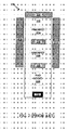
- Figure 5 illustrates yet another exemplary positioning of pads to form an I/O cluster 500 that has multiple pads 502, each with a pmos transistor 516, an nmos transistor 518, and a pad contact 522.
- Each of the pads 502 can also include pad logic circuits 520 (similar to those shown in Figures 3 and 4 ) that provide level shifting, signal receiving, signal driving, or other I/O related functions.
- the I/O cluster 500 also has protection circuits 524 and 526.
- the pads 502 of the I/O cluster 500 arc arranged with like transistors adjacent to each other so that space between pads (such as the spaces 212, 214 and 216 as shown in Figure 2 ) can be eliminated and the pads abutted next to each other without space.
- the I/O cluster 500 can occupy a reduced area while still increasing the number of pads (e.g., pad 502) with contacts (e.g., pad contact 522) provided by the cluster.
- the specific distance between the transistors can be defined by foundry requirements or other manufacturing process requirements.
- Each of the pads also includes the pad contacts 522 which in the illustrated embodiment are disposed on first type edges 508 of the I/O cluster 500 so each pad contact is accessible along the first type edges 508 of the I/O cluster 500.
- first type edge generally refers to an edge of the I/O cluster 500 that includes the pad contacts 522.
- each pad is typically coupled to a solder bump (not shown), to provide an electrical path from the die circuitry through the pad to external circuitry.
- a solder bump not shown
- the risk of forming unwanted parasitic structures with low resistance paths along the first type edges is minimal, because sufficient spacing exists between the nearest transistor (e.g., nmos transistor 518) and the second end (e.g., ends 310 and 312 of Figure 3 ) of the pad.
- the I/O cluster 500 includes multiple pads positioned adjacent to each other and aligned in a first column of pads 504 which may be a single column. Where the I/O cluster 500 is formed using multiple abutting I/O pairs as illustrated in Figure 3 , a second column 506 will be positioned adjacent to the first column 504. In this arrangement, the column 506 is oriented in such a way that the first end of each pad is abutted to the first end of each pad in the first column 504, so that unnecessary space between the pads is eliminated. Aligning the first column 504 and the second column 506 adjacent to each other results in having each pmos transistors positioned adjacent to other pmos transistors, reducing latch up between columns. Aligning the pads in each column also aligns the nmos transistors 518 with adjacent nmos transistors in other pads in the same column, so latch up will likely not occur.
- the I/O cluster 500 can be located on a die in areas with low utilization.
- the I/O cluster 500 can be positioned on the die near other active components, such as I/O clusters or core circuitry.
- the I/O cluster 500 is spaced from other active components (e.g., I/O clusters, core circuitry) by leaving spaces 512 located around second type edges 510 of the I/O cluster, because less protection from latch up is provided at the second type edges 510.
- unwanted parasitic structures with low resistance paths may form in or around the second type edges 510 and increase the risk of latchup and electrostatic damage to the transistors (e.g., pmos transistors 516, nmos transistors 518).
- the phrase "second type edge” generally refers, to an edge of the I/O cluster 500 that is near both pmos and nmos transistor.
- the spaces 512 can be defined by foundry requirements or other manufacturing process requirements that can determine electronic tolerance levels of each device used in the I/O cluster.
- the sizing of the I/O cluster 500 can be defined by power bus resistances found inside the pads 502, and electrostatic discharge tolerance limits of each device in the pads.
- the I/O cluster 500 also may include one or more protection circuits such as protection circuits 524 and 526.
- the protection circuit 524 is shown centrally located in the column 504, so routing distances between the pads and the protection circuit are reduced.
- the protection circuit 524 may be positioned in a different location within the I/O cluster 500.
- the protection circuit 524 can be positioned between a first set of pads 530 and a second set of pads 532, all of which can use a common voltage.
- the protection circuit 524 and the protection circuit 526 electrically couple to the first set of pads 530 and the second set of pads 532, respectively.
- other pads in the I/O cluster 500 can electrically couple to either the protection circuit 524 or the protection circuit 526.
- the protection circuits 524 and 526 are configured to use voltage rails (e.g., pad supply, core supply, or others) according to the devices used in each pad.
- the protection circuits 524 and 526 arc part of the circuits that protect the pads from ESD damage, which can be detrimental to operation of the I/O cluster.
- additional protection circuits can be positioned in the I/O cluster 500 depending on the number of voltage rails present. For example, an integrated circuit can use more than one pad power supply (e.g., 3.3V, 3.6V or others) or core power supply (e.g., 1.5V, 1.8Y or others).
- the protection circuits 524 and 526 can be configured as voltage clamps.
- the I/O cluster 500 and the above-described elements may be varied and are not limited to the functions, structures, configurations, implementations, or examples provided.
- the present disclosure enables efficient floor planning of multiple I/O clusters on a die.
- the I/O clusters can be positioned on any area on the die whether in a low utilized area, or along the edges of the die or on an area with circuitry requiring close proximity.
- the I/O clusters are positioned near high speed circuitry or other types of circuitry that need quick access, or are sensitive to noise or have some other need for close proximity.
- the I/O clusters are spaced from neighboring components using the spaces 512 (shown in Figure 5 ) to prevent latch up.
Landscapes
- Semiconductor Integrated Circuits (AREA)
- Design And Manufacture Of Integrated Circuits (AREA)
- Metal-Oxide And Bipolar Metal-Oxide Semiconductor Integrated Circuits (AREA)
Applications Claiming Priority (3)
| Application Number | Priority Date | Filing Date | Title |
|---|---|---|---|
| US12/182,454 US8184414B2 (en) | 2008-07-30 | 2008-07-30 | Method and apparatus for forming I/O clusters in integrated circuits |
| EP09790496.5A EP2319081B1 (de) | 2008-07-30 | 2009-07-15 | Verfahren und vorrichtung zur bildung von e/a-clustern in integrierten schaltungen |
| PCT/US2009/050752 WO2010014408A2 (en) | 2008-07-30 | 2009-07-15 | Method and apparatus for forming i/o clusters in integrated circuits |
Related Parent Applications (3)
| Application Number | Title | Priority Date | Filing Date |
|---|---|---|---|
| EP09790496.5 Division | 2009-07-15 | ||
| EP09790496.5A Division-Into EP2319081B1 (de) | 2008-07-30 | 2009-07-15 | Verfahren und vorrichtung zur bildung von e/a-clustern in integrierten schaltungen |
| EP09790496.5A Division EP2319081B1 (de) | 2008-07-30 | 2009-07-15 | Verfahren und vorrichtung zur bildung von e/a-clustern in integrierten schaltungen |
Publications (2)
| Publication Number | Publication Date |
|---|---|
| EP2372767A1 true EP2372767A1 (de) | 2011-10-05 |
| EP2372767B1 EP2372767B1 (de) | 2021-09-08 |
Family
ID=41226838
Family Applications (3)
| Application Number | Title | Priority Date | Filing Date |
|---|---|---|---|
| EP21190681.3A Active EP3961709B1 (de) | 2008-07-30 | 2009-07-15 | Integrierte-schaltung-chip mit einer eingang/ausgang-gruppe |
| EP11169152.3A Active EP2372767B1 (de) | 2008-07-30 | 2009-07-15 | Verfahren zur bildung von e/a-clustern in integrierten schaltungen und entsprechende e/a-cluster |
| EP09790496.5A Active EP2319081B1 (de) | 2008-07-30 | 2009-07-15 | Verfahren und vorrichtung zur bildung von e/a-clustern in integrierten schaltungen |
Family Applications Before (1)
| Application Number | Title | Priority Date | Filing Date |
|---|---|---|---|
| EP21190681.3A Active EP3961709B1 (de) | 2008-07-30 | 2009-07-15 | Integrierte-schaltung-chip mit einer eingang/ausgang-gruppe |
Family Applications After (1)
| Application Number | Title | Priority Date | Filing Date |
|---|---|---|---|
| EP09790496.5A Active EP2319081B1 (de) | 2008-07-30 | 2009-07-15 | Verfahren und vorrichtung zur bildung von e/a-clustern in integrierten schaltungen |
Country Status (8)
| Country | Link |
|---|---|
| US (1) | US8184414B2 (de) |
| EP (3) | EP3961709B1 (de) |
| JP (2) | JP5855458B2 (de) |
| KR (1) | KR101301192B1 (de) |
| CN (1) | CN102099912B (de) |
| ES (2) | ES2889760T3 (de) |
| TW (1) | TW201019462A (de) |
| WO (1) | WO2010014408A2 (de) |
Families Citing this family (2)
| Publication number | Priority date | Publication date | Assignee | Title |
|---|---|---|---|---|
| WO2017169150A1 (ja) * | 2016-03-28 | 2017-10-05 | 株式会社ソシオネクスト | 半導体集積回路装置 |
| US11688686B2 (en) | 2020-07-14 | 2023-06-27 | Samsung Electronics Co., Ltd. | Semiconductor device including an input/output circuit |
Citations (9)
| Publication number | Priority date | Publication date | Assignee | Title |
|---|---|---|---|---|
| US5051917A (en) * | 1987-02-24 | 1991-09-24 | International Business Machines Corporation | Method of combining gate array and standard cell circuits on a common semiconductor chip |
| GB2299705A (en) * | 1995-04-06 | 1996-10-09 | Samsung Electronics Co Ltd | Semiconductor device |
| US5828110A (en) * | 1995-06-05 | 1998-10-27 | Advanced Micro Devices, Inc. | Latchup-proof I/O circuit implementation |
| US20020130332A1 (en) * | 2001-03-12 | 2002-09-19 | Samsung Electronics Co., Ltd. | Layout method of latch-up prevention circuit of a semiconductor device |
| JP2004119744A (ja) * | 2002-09-27 | 2004-04-15 | Matsushita Electric Ind Co Ltd | 半導体装置の設計方法 |
| US6836026B1 (en) * | 2003-01-14 | 2004-12-28 | Lsi Logic Corporation | Integrated circuit design for both input output limited and core limited integrated circuits |
| US20060249842A1 (en) * | 2005-03-30 | 2006-11-09 | Elpida Memory, Inc | Semiconductor device |
| US20070007545A1 (en) * | 2005-07-07 | 2007-01-11 | Intersil Americas Inc. | Devices with adjustable dual-polarity trigger- and holding-voltage/current for high level of electrostatic discharge protection in sub-micron mixed signal CMOS/BiCMOS integrated circuits |
| US20070267748A1 (en) * | 2006-05-16 | 2007-11-22 | Tran Tu-Anh N | Integrated circuit having pads and input/output (i/o) cells |
Family Cites Families (13)
| Publication number | Priority date | Publication date | Assignee | Title |
|---|---|---|---|---|
| JPS58107648A (ja) * | 1981-12-21 | 1983-06-27 | Nec Corp | 集積回路装置 |
| KR910020888A (ko) * | 1990-05-25 | 1991-12-20 | 김광호 | 반도체 칩의 정전기 보호회로 |
| JPH04336812A (ja) * | 1991-05-14 | 1992-11-25 | Nec Home Electron Ltd | デジタル回路装置 |
| JPH098227A (ja) * | 1995-06-16 | 1997-01-10 | Fujitsu Ltd | 半導体集積回路装置 |
| KR970058476A (ko) * | 1995-12-29 | 1997-07-31 | 김광호 | 반도체 칩의 정전기 보호 장치 |
| JP3134829B2 (ja) * | 1997-11-12 | 2001-02-13 | 日本電気株式会社 | 半導体装置 |
| JP2001237322A (ja) | 2000-02-25 | 2001-08-31 | Nec Microsystems Ltd | 半導体集積回路のレイアウト方法 |
| US6849902B1 (en) * | 2004-03-11 | 2005-02-01 | Winbond Electronics Corp. | Input/output cell with robust electrostatic discharge protection |
| JP2006100436A (ja) * | 2004-09-28 | 2006-04-13 | Toshiba Corp | 半導体装置 |
| JP2006128422A (ja) * | 2004-10-29 | 2006-05-18 | Renesas Technology Corp | 半導体集積回路 |
| JP2007227665A (ja) * | 2006-02-23 | 2007-09-06 | Ricoh Co Ltd | 半導体集積回路装置 |
| US7594198B2 (en) * | 2007-02-27 | 2009-09-22 | Taiwan Semiconductor Manufacturing Co., Ltd. | Ultra fine pitch I/O design for microchips |
| US7772887B2 (en) * | 2008-07-29 | 2010-08-10 | Qualcomm Incorporated | High signal level compliant input/output circuits |
-
2008
- 2008-07-30 US US12/182,454 patent/US8184414B2/en active Active
-
2009
- 2009-07-15 JP JP2011521174A patent/JP5855458B2/ja active Active
- 2009-07-15 EP EP21190681.3A patent/EP3961709B1/de active Active
- 2009-07-15 EP EP11169152.3A patent/EP2372767B1/de active Active
- 2009-07-15 KR KR1020117004449A patent/KR101301192B1/ko not_active Expired - Fee Related
- 2009-07-15 WO PCT/US2009/050752 patent/WO2010014408A2/en not_active Ceased
- 2009-07-15 EP EP09790496.5A patent/EP2319081B1/de active Active
- 2009-07-15 ES ES11169152T patent/ES2889760T3/es active Active
- 2009-07-15 ES ES09790496T patent/ES2901897T3/es active Active
- 2009-07-15 CN CN2009801277273A patent/CN102099912B/zh active Active
- 2009-07-24 TW TW098125075A patent/TW201019462A/zh unknown
-
2014
- 2014-03-26 JP JP2014064458A patent/JP2014150272A/ja active Pending
Patent Citations (9)
| Publication number | Priority date | Publication date | Assignee | Title |
|---|---|---|---|---|
| US5051917A (en) * | 1987-02-24 | 1991-09-24 | International Business Machines Corporation | Method of combining gate array and standard cell circuits on a common semiconductor chip |
| GB2299705A (en) * | 1995-04-06 | 1996-10-09 | Samsung Electronics Co Ltd | Semiconductor device |
| US5828110A (en) * | 1995-06-05 | 1998-10-27 | Advanced Micro Devices, Inc. | Latchup-proof I/O circuit implementation |
| US20020130332A1 (en) * | 2001-03-12 | 2002-09-19 | Samsung Electronics Co., Ltd. | Layout method of latch-up prevention circuit of a semiconductor device |
| JP2004119744A (ja) * | 2002-09-27 | 2004-04-15 | Matsushita Electric Ind Co Ltd | 半導体装置の設計方法 |
| US6836026B1 (en) * | 2003-01-14 | 2004-12-28 | Lsi Logic Corporation | Integrated circuit design for both input output limited and core limited integrated circuits |
| US20060249842A1 (en) * | 2005-03-30 | 2006-11-09 | Elpida Memory, Inc | Semiconductor device |
| US20070007545A1 (en) * | 2005-07-07 | 2007-01-11 | Intersil Americas Inc. | Devices with adjustable dual-polarity trigger- and holding-voltage/current for high level of electrostatic discharge protection in sub-micron mixed signal CMOS/BiCMOS integrated circuits |
| US20070267748A1 (en) * | 2006-05-16 | 2007-11-22 | Tran Tu-Anh N | Integrated circuit having pads and input/output (i/o) cells |
Also Published As
| Publication number | Publication date |
|---|---|
| CN102099912B (zh) | 2013-06-05 |
| EP2319081B1 (de) | 2021-11-24 |
| JP2011530171A (ja) | 2011-12-15 |
| EP2372767B1 (de) | 2021-09-08 |
| US8184414B2 (en) | 2012-05-22 |
| EP3961709B1 (de) | 2026-04-15 |
| JP5855458B2 (ja) | 2016-02-09 |
| WO2010014408A2 (en) | 2010-02-04 |
| CN102099912A (zh) | 2011-06-15 |
| EP3961709A1 (de) | 2022-03-02 |
| KR101301192B1 (ko) | 2013-08-29 |
| TW201019462A (en) | 2010-05-16 |
| US20100027171A1 (en) | 2010-02-04 |
| ES2889760T3 (es) | 2022-01-13 |
| WO2010014408A3 (en) | 2010-08-05 |
| KR20110039567A (ko) | 2011-04-19 |
| EP2319081A2 (de) | 2011-05-11 |
| ES2901897T3 (es) | 2022-03-24 |
| JP2014150272A (ja) | 2014-08-21 |
Similar Documents
| Publication | Publication Date | Title |
|---|---|---|
| US8604626B2 (en) | Reduced susceptibility to electrostatic discharge during 3D semiconductor device bonding and assembly | |
| EP1897138B1 (de) | Halbleitervorrichtung und dazugehörige Montagestruktur | |
| US9299673B2 (en) | Method for manufacturing a semiconductor chip with each contact pad having a pad cell associated therewith | |
| US8115321B2 (en) | Separate probe and bond regions of an integrated circuit | |
| JP4652703B2 (ja) | 半導体回路装置及びマルチ・チップ・パッケージ | |
| US7808117B2 (en) | Integrated circuit having pads and input/output (I/O) cells | |
| US7250660B1 (en) | ESD protection that supports LVDS and OCT | |
| EP2372767B1 (de) | Verfahren zur bildung von e/a-clustern in integrierten schaltungen und entsprechende e/a-cluster | |
| US8531806B2 (en) | Distributed building blocks of R-C clamping circuitry in semiconductor die core area | |
| US20070267748A1 (en) | Integrated circuit having pads and input/output (i/o) cells | |
| US8154117B2 (en) | High power integrated circuit device having bump pads | |
| US20250006726A1 (en) | Serial interface providing electrostatic discharge protection | |
| US12484312B2 (en) | Semiconductor integrated circuit device | |
| HK1229065A1 (en) | Split thin film capacitor for multiple voltages | |
| JP2015056420A (ja) | Esd保護回路 |
Legal Events
| Date | Code | Title | Description |
|---|---|---|---|
| PUAI | Public reference made under article 153(3) epc to a published international application that has entered the european phase |
Free format text: ORIGINAL CODE: 0009012 |
|
| AC | Divisional application: reference to earlier application |
Ref document number: 2319081 Country of ref document: EP Kind code of ref document: P |
|
| AK | Designated contracting states |
Kind code of ref document: A1 Designated state(s): AT BE BG CH CY CZ DE DK EE ES FI FR GB GR HR HU IE IS IT LI LT LU LV MC MK MT NL NO PL PT RO SE SI SK SM TR |
|
| 17P | Request for examination filed |
Effective date: 20120329 |
|
| STAA | Information on the status of an ep patent application or granted ep patent |
Free format text: STATUS: EXAMINATION IS IN PROGRESS |
|
| 17Q | First examination report despatched |
Effective date: 20170717 |
|
| REG | Reference to a national code |
Ref country code: DE Ref legal event code: R079 Ref document number: 602009064019 Country of ref document: DE Free format text: PREVIOUS MAIN CLASS: H01L0027092000 Ipc: H01L0021823800 |
|
| GRAP | Despatch of communication of intention to grant a patent |
Free format text: ORIGINAL CODE: EPIDOSNIGR1 |
|
| STAA | Information on the status of an ep patent application or granted ep patent |
Free format text: STATUS: GRANT OF PATENT IS INTENDED |
|
| RIC1 | Information provided on ipc code assigned before grant |
Ipc: H01L 21/8238 20060101AFI20210301BHEP Ipc: H03K 19/003 20060101ALI20210301BHEP Ipc: H01L 27/092 20060101ALI20210301BHEP Ipc: H01L 27/02 20060101ALI20210301BHEP Ipc: H01L 23/00 20060101ALI20210301BHEP Ipc: H01L 23/50 20060101ALI20210301BHEP |
|
| INTG | Intention to grant announced |
Effective date: 20210330 |
|
| GRAS | Grant fee paid |
Free format text: ORIGINAL CODE: EPIDOSNIGR3 |
|
| GRAA | (expected) grant |
Free format text: ORIGINAL CODE: 0009210 |
|
| STAA | Information on the status of an ep patent application or granted ep patent |
Free format text: STATUS: THE PATENT HAS BEEN GRANTED |
|
| AC | Divisional application: reference to earlier application |
Ref document number: 2319081 Country of ref document: EP Kind code of ref document: P |
|
| AK | Designated contracting states |
Kind code of ref document: B1 Designated state(s): AT BE BG CH CY CZ DE DK EE ES FI FR GB GR HR HU IE IS IT LI LT LU LV MC MK MT NL NO PL PT RO SE SI SK SM TR |
|
| REG | Reference to a national code |
Ref country code: GB Ref legal event code: FG4D |
|
| REG | Reference to a national code |
Ref country code: CH Ref legal event code: EP Ref country code: AT Ref legal event code: REF Ref document number: 1429340 Country of ref document: AT Kind code of ref document: T Effective date: 20210915 |
|
| REG | Reference to a national code |
Ref country code: DE Ref legal event code: R096 Ref document number: 602009064019 Country of ref document: DE |
|
| REG | Reference to a national code |
Ref country code: IE Ref legal event code: FG4D |
|
| REG | Reference to a national code |
Ref country code: SE Ref legal event code: TRGR |
|
| REG | Reference to a national code |
Ref country code: NL Ref legal event code: FP |
|
| REG | Reference to a national code |
Ref country code: LT Ref legal event code: MG9D |
|
| REG | Reference to a national code |
Ref country code: ES Ref legal event code: FG2A Ref document number: 2889760 Country of ref document: ES Kind code of ref document: T3 Effective date: 20220113 |
|
| PG25 | Lapsed in a contracting state [announced via postgrant information from national office to epo] |
Ref country code: HR Free format text: LAPSE BECAUSE OF FAILURE TO SUBMIT A TRANSLATION OF THE DESCRIPTION OR TO PAY THE FEE WITHIN THE PRESCRIBED TIME-LIMIT Effective date: 20210908 Ref country code: BG Free format text: LAPSE BECAUSE OF FAILURE TO SUBMIT A TRANSLATION OF THE DESCRIPTION OR TO PAY THE FEE WITHIN THE PRESCRIBED TIME-LIMIT Effective date: 20211208 Ref country code: LT Free format text: LAPSE BECAUSE OF FAILURE TO SUBMIT A TRANSLATION OF THE DESCRIPTION OR TO PAY THE FEE WITHIN THE PRESCRIBED TIME-LIMIT Effective date: 20210908 Ref country code: NO Free format text: LAPSE BECAUSE OF FAILURE TO SUBMIT A TRANSLATION OF THE DESCRIPTION OR TO PAY THE FEE WITHIN THE PRESCRIBED TIME-LIMIT Effective date: 20211208 Ref country code: FI Free format text: LAPSE BECAUSE OF FAILURE TO SUBMIT A TRANSLATION OF THE DESCRIPTION OR TO PAY THE FEE WITHIN THE PRESCRIBED TIME-LIMIT Effective date: 20210908 |
|
| REG | Reference to a national code |
Ref country code: AT Ref legal event code: MK05 Ref document number: 1429340 Country of ref document: AT Kind code of ref document: T Effective date: 20210908 |
|
| PG25 | Lapsed in a contracting state [announced via postgrant information from national office to epo] |
Ref country code: LV Free format text: LAPSE BECAUSE OF FAILURE TO SUBMIT A TRANSLATION OF THE DESCRIPTION OR TO PAY THE FEE WITHIN THE PRESCRIBED TIME-LIMIT Effective date: 20210908 Ref country code: GR Free format text: LAPSE BECAUSE OF FAILURE TO SUBMIT A TRANSLATION OF THE DESCRIPTION OR TO PAY THE FEE WITHIN THE PRESCRIBED TIME-LIMIT Effective date: 20211209 |
|
| PG25 | Lapsed in a contracting state [announced via postgrant information from national office to epo] |
Ref country code: AT Free format text: LAPSE BECAUSE OF FAILURE TO SUBMIT A TRANSLATION OF THE DESCRIPTION OR TO PAY THE FEE WITHIN THE PRESCRIBED TIME-LIMIT Effective date: 20210908 |
|
| PG25 | Lapsed in a contracting state [announced via postgrant information from national office to epo] |
Ref country code: IS Free format text: LAPSE BECAUSE OF FAILURE TO SUBMIT A TRANSLATION OF THE DESCRIPTION OR TO PAY THE FEE WITHIN THE PRESCRIBED TIME-LIMIT Effective date: 20220108 Ref country code: SM Free format text: LAPSE BECAUSE OF FAILURE TO SUBMIT A TRANSLATION OF THE DESCRIPTION OR TO PAY THE FEE WITHIN THE PRESCRIBED TIME-LIMIT Effective date: 20210908 Ref country code: SK Free format text: LAPSE BECAUSE OF FAILURE TO SUBMIT A TRANSLATION OF THE DESCRIPTION OR TO PAY THE FEE WITHIN THE PRESCRIBED TIME-LIMIT Effective date: 20210908 Ref country code: RO Free format text: LAPSE BECAUSE OF FAILURE TO SUBMIT A TRANSLATION OF THE DESCRIPTION OR TO PAY THE FEE WITHIN THE PRESCRIBED TIME-LIMIT Effective date: 20210908 Ref country code: PT Free format text: LAPSE BECAUSE OF FAILURE TO SUBMIT A TRANSLATION OF THE DESCRIPTION OR TO PAY THE FEE WITHIN THE PRESCRIBED TIME-LIMIT Effective date: 20220110 Ref country code: PL Free format text: LAPSE BECAUSE OF FAILURE TO SUBMIT A TRANSLATION OF THE DESCRIPTION OR TO PAY THE FEE WITHIN THE PRESCRIBED TIME-LIMIT Effective date: 20210908 Ref country code: EE Free format text: LAPSE BECAUSE OF FAILURE TO SUBMIT A TRANSLATION OF THE DESCRIPTION OR TO PAY THE FEE WITHIN THE PRESCRIBED TIME-LIMIT Effective date: 20210908 Ref country code: CZ Free format text: LAPSE BECAUSE OF FAILURE TO SUBMIT A TRANSLATION OF THE DESCRIPTION OR TO PAY THE FEE WITHIN THE PRESCRIBED TIME-LIMIT Effective date: 20210908 |
|
| REG | Reference to a national code |
Ref country code: DE Ref legal event code: R097 Ref document number: 602009064019 Country of ref document: DE |
|
| PLBE | No opposition filed within time limit |
Free format text: ORIGINAL CODE: 0009261 |
|
| STAA | Information on the status of an ep patent application or granted ep patent |
Free format text: STATUS: NO OPPOSITION FILED WITHIN TIME LIMIT |
|
| PG25 | Lapsed in a contracting state [announced via postgrant information from national office to epo] |
Ref country code: DK Free format text: LAPSE BECAUSE OF FAILURE TO SUBMIT A TRANSLATION OF THE DESCRIPTION OR TO PAY THE FEE WITHIN THE PRESCRIBED TIME-LIMIT Effective date: 20210908 |
|
| 26N | No opposition filed |
Effective date: 20220609 |
|
| PG25 | Lapsed in a contracting state [announced via postgrant information from national office to epo] |
Ref country code: SI Free format text: LAPSE BECAUSE OF FAILURE TO SUBMIT A TRANSLATION OF THE DESCRIPTION OR TO PAY THE FEE WITHIN THE PRESCRIBED TIME-LIMIT Effective date: 20210908 |
|
| PG25 | Lapsed in a contracting state [announced via postgrant information from national office to epo] |
Ref country code: MC Free format text: LAPSE BECAUSE OF FAILURE TO SUBMIT A TRANSLATION OF THE DESCRIPTION OR TO PAY THE FEE WITHIN THE PRESCRIBED TIME-LIMIT Effective date: 20210908 |
|
| REG | Reference to a national code |
Ref country code: BE Ref legal event code: MM Effective date: 20220731 |
|
| PG25 | Lapsed in a contracting state [announced via postgrant information from national office to epo] |
Ref country code: LU Free format text: LAPSE BECAUSE OF NON-PAYMENT OF DUE FEES Effective date: 20220715 |
|
| PG25 | Lapsed in a contracting state [announced via postgrant information from national office to epo] |
Ref country code: BE Free format text: LAPSE BECAUSE OF NON-PAYMENT OF DUE FEES Effective date: 20220731 |
|
| PG25 | Lapsed in a contracting state [announced via postgrant information from national office to epo] |
Ref country code: IE Free format text: LAPSE BECAUSE OF NON-PAYMENT OF DUE FEES Effective date: 20220715 |
|
| PG25 | Lapsed in a contracting state [announced via postgrant information from national office to epo] |
Ref country code: HU Free format text: LAPSE BECAUSE OF FAILURE TO SUBMIT A TRANSLATION OF THE DESCRIPTION OR TO PAY THE FEE WITHIN THE PRESCRIBED TIME-LIMIT; INVALID AB INITIO Effective date: 20090715 |
|
| PG25 | Lapsed in a contracting state [announced via postgrant information from national office to epo] |
Ref country code: MK Free format text: LAPSE BECAUSE OF FAILURE TO SUBMIT A TRANSLATION OF THE DESCRIPTION OR TO PAY THE FEE WITHIN THE PRESCRIBED TIME-LIMIT Effective date: 20210908 Ref country code: CY Free format text: LAPSE BECAUSE OF FAILURE TO SUBMIT A TRANSLATION OF THE DESCRIPTION OR TO PAY THE FEE WITHIN THE PRESCRIBED TIME-LIMIT Effective date: 20210908 |
|
| PG25 | Lapsed in a contracting state [announced via postgrant information from national office to epo] |
Ref country code: TR Free format text: LAPSE BECAUSE OF FAILURE TO SUBMIT A TRANSLATION OF THE DESCRIPTION OR TO PAY THE FEE WITHIN THE PRESCRIBED TIME-LIMIT Effective date: 20210908 |
|
| PGFP | Annual fee paid to national office [announced via postgrant information from national office to epo] |
Ref country code: NL Payment date: 20240617 Year of fee payment: 16 |
|
| PG25 | Lapsed in a contracting state [announced via postgrant information from national office to epo] |
Ref country code: MT Free format text: LAPSE BECAUSE OF FAILURE TO SUBMIT A TRANSLATION OF THE DESCRIPTION OR TO PAY THE FEE WITHIN THE PRESCRIBED TIME-LIMIT Effective date: 20210908 |
|
| PGFP | Annual fee paid to national office [announced via postgrant information from national office to epo] |
Ref country code: ES Payment date: 20240807 Year of fee payment: 16 Ref country code: CH Payment date: 20240801 Year of fee payment: 16 |
|
| PGFP | Annual fee paid to national office [announced via postgrant information from national office to epo] |
Ref country code: IT Payment date: 20240710 Year of fee payment: 16 Ref country code: SE Payment date: 20240708 Year of fee payment: 16 |
|
| REG | Reference to a national code |
Ref country code: DE Ref legal event code: R079 Ref document number: 602009064019 Country of ref document: DE Free format text: PREVIOUS MAIN CLASS: H01L0021823800 Ipc: H10D0084850000 |
|
| PGFP | Annual fee paid to national office [announced via postgrant information from national office to epo] |
Ref country code: GB Payment date: 20250612 Year of fee payment: 17 |
|
| PGFP | Annual fee paid to national office [announced via postgrant information from national office to epo] |
Ref country code: FR Payment date: 20250612 Year of fee payment: 17 |
|
| PGFP | Annual fee paid to national office [announced via postgrant information from national office to epo] |
Ref country code: DE Payment date: 20250616 Year of fee payment: 17 |
|
| REG | Reference to a national code |
Ref country code: CH Ref legal event code: H13 Free format text: ST27 STATUS EVENT CODE: U-0-0-H10-H13 (AS PROVIDED BY THE NATIONAL OFFICE) Effective date: 20260224 |
|
| REG | Reference to a national code |
Ref country code: NL Ref legal event code: MM Effective date: 20250801 |
|
| PG25 | Lapsed in a contracting state [announced via postgrant information from national office to epo] |
Ref country code: NL Free format text: LAPSE BECAUSE OF NON-PAYMENT OF DUE FEES Effective date: 20250801 |
|
| PG25 | Lapsed in a contracting state [announced via postgrant information from national office to epo] |
Ref country code: CH Free format text: LAPSE BECAUSE OF NON-PAYMENT OF DUE FEES Effective date: 20250731 |