EP2372905A1 - Doherty-Verstärkeranordnung mit verbessertem Wirkungsgrad - Google Patents
Doherty-Verstärkeranordnung mit verbessertem Wirkungsgrad Download PDFInfo
- Publication number
- EP2372905A1 EP2372905A1 EP10290175A EP10290175A EP2372905A1 EP 2372905 A1 EP2372905 A1 EP 2372905A1 EP 10290175 A EP10290175 A EP 10290175A EP 10290175 A EP10290175 A EP 10290175A EP 2372905 A1 EP2372905 A1 EP 2372905A1
- Authority
- EP
- European Patent Office
- Prior art keywords
- amplifier
- supply voltage
- peak
- doherty
- main
- Prior art date
- Legal status (The legal status is an assumption and is not a legal conclusion. Google has not performed a legal analysis and makes no representation as to the accuracy of the status listed.)
- Granted
Links
- 230000003321 amplification Effects 0.000 claims abstract description 28
- 238000003199 nucleic acid amplification method Methods 0.000 claims abstract description 28
- 238000000034 method Methods 0.000 claims abstract description 15
- 238000004590 computer program Methods 0.000 claims description 3
- 238000013459 approach Methods 0.000 description 9
- 230000006978 adaptation Effects 0.000 description 8
- 238000010586 diagram Methods 0.000 description 7
- 230000006870 function Effects 0.000 description 7
- 230000006872 improvement Effects 0.000 description 5
- 230000003044 adaptive effect Effects 0.000 description 4
- 230000001419 dependent effect Effects 0.000 description 3
- 230000005540 biological transmission Effects 0.000 description 2
- 238000006243 chemical reaction Methods 0.000 description 2
- 230000005669 field effect Effects 0.000 description 2
- 230000003247 decreasing effect Effects 0.000 description 1
- 230000000694 effects Effects 0.000 description 1
- 238000002474 experimental method Methods 0.000 description 1
- 230000003993 interaction Effects 0.000 description 1
- 238000013507 mapping Methods 0.000 description 1
- 230000008569 process Effects 0.000 description 1
- 230000007704 transition Effects 0.000 description 1
Images
Classifications
-
- H—ELECTRICITY
- H03—ELECTRONIC CIRCUITRY
- H03F—AMPLIFIERS
- H03F1/00—Details of amplifiers with only discharge tubes, only semiconductor devices or only unspecified devices as amplifying elements
- H03F1/02—Modifications of amplifiers to raise the efficiency, e.g. gliding Class A stages, use of an auxiliary oscillation
- H03F1/0205—Modifications of amplifiers to raise the efficiency, e.g. gliding Class A stages, use of an auxiliary oscillation in transistor amplifiers
- H03F1/0288—Modifications of amplifiers to raise the efficiency, e.g. gliding Class A stages, use of an auxiliary oscillation in transistor amplifiers using a main and one or several auxiliary peaking amplifiers whereby the load is connected to the main amplifier using an impedance inverter, e.g. Doherty amplifiers
-
- H—ELECTRICITY
- H03—ELECTRONIC CIRCUITRY
- H03F—AMPLIFIERS
- H03F1/00—Details of amplifiers with only discharge tubes, only semiconductor devices or only unspecified devices as amplifying elements
- H03F1/02—Modifications of amplifiers to raise the efficiency, e.g. gliding Class A stages, use of an auxiliary oscillation
- H03F1/0205—Modifications of amplifiers to raise the efficiency, e.g. gliding Class A stages, use of an auxiliary oscillation in transistor amplifiers
- H03F1/0211—Modifications of amplifiers to raise the efficiency, e.g. gliding Class A stages, use of an auxiliary oscillation in transistor amplifiers with control of the supply voltage or current
- H03F1/0244—Stepped control
-
- H—ELECTRICITY
- H03—ELECTRONIC CIRCUITRY
- H03F—AMPLIFIERS
- H03F1/00—Details of amplifiers with only discharge tubes, only semiconductor devices or only unspecified devices as amplifying elements
- H03F1/02—Modifications of amplifiers to raise the efficiency, e.g. gliding Class A stages, use of an auxiliary oscillation
- H03F1/0205—Modifications of amplifiers to raise the efficiency, e.g. gliding Class A stages, use of an auxiliary oscillation in transistor amplifiers
- H03F1/0261—Modifications of amplifiers to raise the efficiency, e.g. gliding Class A stages, use of an auxiliary oscillation in transistor amplifiers with control of the polarisation voltage or current, e.g. gliding Class A
- H03F1/0266—Modifications of amplifiers to raise the efficiency, e.g. gliding Class A stages, use of an auxiliary oscillation in transistor amplifiers with control of the polarisation voltage or current, e.g. gliding Class A by using a signal derived from the input signal
-
- H—ELECTRICITY
- H03—ELECTRONIC CIRCUITRY
- H03F—AMPLIFIERS
- H03F3/00—Amplifiers with only discharge tubes or only semiconductor devices as amplifying elements
- H03F3/20—Power amplifiers, e.g. Class B amplifiers, Class C amplifiers
- H03F3/24—Power amplifiers, e.g. Class B amplifiers, Class C amplifiers of transmitter output stages
-
- H—ELECTRICITY
- H03—ELECTRONIC CIRCUITRY
- H03G—CONTROL OF AMPLIFICATION
- H03G3/00—Gain control in amplifiers or frequency changers
- H03G3/004—Control by varying the supply voltage
-
- H—ELECTRICITY
- H03—ELECTRONIC CIRCUITRY
- H03F—AMPLIFIERS
- H03F2200/00—Indexing scheme relating to amplifiers
- H03F2200/15—Indexing scheme relating to amplifiers the supply or bias voltage or current at the drain side of a FET being continuously controlled by a controlling signal
-
- H—ELECTRICITY
- H03—ELECTRONIC CIRCUITRY
- H03F—AMPLIFIERS
- H03F2200/00—Indexing scheme relating to amplifiers
- H03F2200/18—Indexing scheme relating to amplifiers the bias of the gate of a FET being controlled by a control signal
-
- H—ELECTRICITY
- H03—ELECTRONIC CIRCUITRY
- H03F—AMPLIFIERS
- H03F2200/00—Indexing scheme relating to amplifiers
- H03F2200/511—Many discrete supply voltages or currents or voltage levels can be chosen by a control signal in an IC-block amplifier circuit
Definitions
- the invention relates to the field of telecommunications, and, more specifically, to efficiency improvements of Doherty amplifiers used for signal amplification e.g. in base stations of wireless communications networks.
- Doherty amplifiers typically comprise two parallel amplification paths for an input signal: A main amplification path with a main amplifier biased to work in class A/B mode, and an auxiliary amplification path with a peak amplifier biased to operate in class C mode, as well as two quarter-wave sections, each being arranged in a respective amplification path.
- a main amplification path with a main amplifier biased to work in class A/B mode and an auxiliary amplification path with a peak amplifier biased to operate in class C mode, as well as two quarter-wave sections, each being arranged in a respective amplification path.
- the main amplifier saturates and the peak amplifier takes over.
- a Doherty amplifier provides a high power-added efficiency with input signals that have high peak-to-average ratios.
- one approach for improving efficiency would be switching a supply voltage (drain-source voltage when a Field Effect Transistor (FET) is used) of the main amplifier depending on the load condition (e.g. daytime - nighttime), or alternatively adapting the input supply voltage (gate-source voltage for a FET) of the peak transistor.
- FET Field Effect Transistor
- Both mentioned approaches improve efficiency, but still with clear room for improvement as compared to the theoretical Doherty limits.
- concepts like Envelope Tracking based on bias modulation of conventional Class-AB amplifiers are known, supplying the Class-AB amplifier with a modulation voltage depending on the envelope signal and the load condition of the Class-AB amplifier.
- a specific supply voltage modulator is required which is challenging to implement.
- the present invention is directed to addressing the effects of one or more of the problems set forth above.
- the following presents a simplified summary of the invention in order to provide a basic understanding of some aspects of the invention. This summary is not an exhaustive overview of the invention. It is not intended to identify key or critical elements of the invention or to delineate the scope of the invention. Its sole purpose is to present some concepts in a simplified form as a prelude to the more detailed description that is discussed later.
- One aspect of the invention relates to a Doherty amplifier arrangement for amplification of an RF signal, comprising: a main amplification path with a main amplifier, a main amplifier control unit for switching a supply voltage of the main amplifier in dependence of a load condition of the Doherty amplifier arrangement, an auxiliary amplification path with a peak amplifier, and a peak amplifier control unit for modulating an input supply voltage of the peak amplifier in dependence of an envelope of the input signal.
- the inventors propose to combine switching the (output) supply voltage of the main amplifier and typically also of the peak amplifier between different discrete values in dependence of the load (realizing a comparatively slow adaptation) with a signal-envelope related modulation of an input supply voltage provided to the peak amplifier (realizing a comparatively fast adaptation with quasi-continuous voltage levels).
- the efficiency at low to high back-off operation i.e. for different load situations
- the peak efficiency of the Doherty amplifier arrangement can be improved.
- a common Doherty amplifier concept can be realized which leads to an additionally improved efficiency as compared to the single approaches.
- the peak amplifier control unit is adapted for modulating the input supply voltage of the peak amplifier also in dependence of a load condition and/or of a quality of an output signal of the Doherty amplifier arrangement.
- the input supply voltage may also be chosen in dependence of the load condition and/or on the output signal of the Doherty amplifier.
- a plurality of functions may be used, each function being defined for a different load condition / quality of the output signal.
- the Doherty amplifier arrangement is adapted for switching the supply voltage of the main amplifier and for modulating the input supply voltage of the peak amplifier in a coordinated way.
- the supply voltage of the main amplifier (and of the peak amplifier) as well as the input supply voltage of the peak amplifier are switched / adapted in dependence of the load, resulting in a load-dependent coordination of both approaches. For instance, for each discrete value of the supply voltage of the main/auxiliary amplifier (typically corresponding to a different load scenario chosen from a discrete set of load scenarios), a different relation / function relating the envelope signal to the input supply voltage may be used.
- At least one of the peak amplifier control unit and the main amplifier control unit are further adapted for switching an output supply voltage of the peak amplifier in dependence of a load condition of the Doherty amplifier arrangement.
- the output supply voltage e.g. drain-source voltage of a FET
- the output supply voltage will be switched only in dependence of the load condition, i.e. the output supply voltage will also be chosen from a discrete set of values (in general not more than ten values, typically five or less values, corresponding to different load scenarios).
- the peak amplifier control unit comprises at least one look-up table relating the input supply voltage to the envelope of the input signal.
- a look-up table may be used for quickly determining a current value of the input supply voltage from a plurality of parameters (signal envelope, load, possibly output signal quality).
- the Doherty amplifier arrangement comprises a plurality of look-up tables, each for a different load condition of the Doherty amplifier arrangement. For instance, three look-up tables may be provided a first one for a low load scenario, a second one for a mid load scenario, and a third one for a high load scenario, respectively.
- the look-up tables may be implemented e.g. in a Field Programmable Gate Array, FPGA, or other suitable device.
- a suitable interface adaptation and an adaptive power supply may be used to provide the adaptive input supply voltage to the peak amplifier.
- further input parameters may be provided, so that a plurality of look-up tables may be used, each look-up table corresponding to a specific combination of the input parameters.
- the main amplifier control unit comprises a switchable power supply for generating a plurality of discrete voltage levels to be provided as supply voltages to the main amplifier. For instance, for the low, mid, and high load scenario, a voltage level of e.g. 15 V, 20 V, or 30 V may be used.
- the switchable (DC) power supply may e.g. comprise a DC-to-DC converter for switching between the different voltage levels. Typically, the switching between the discrete voltage levels is performed at a switching frequency smaller than 100 kHz.
- the switchable power supply of the main amplifier control unit may also be used for providing the (output) supply voltage for the peak amplifier. In this case, the (output) supply voltage provided to the main amplifier and the peak amplifier will be identical and both will be switched e.g. between the three voltage levels of 15 V, 20 V, or 30 V, respectively.
- a further aspect of the invention relates to a transmit frontend for a base station, comprising a Doherty amplifier arrangement as described above.
- the transmit frontend typically has a digital frontend unit which is adapted to generate a (digital) baseband signal which is Analog-to-Digital converted before being up-converted to the RF domain, the up-converted signal being provided to the Doherty amplifier arrangement as an input signal for amplification.
- the output signal after amplification will then be provided to an antenna for radio transmissions (via a suitable antenna network).
- the digital frontend As the digital frontend generates the input signal, the digital frontend typically has both the information about the load condition and the envelope of the input signal which is provided to the Doherty amplifier arrangement, such that it is ideally suited for implementing at least part of the main amplifier control unit and the peak amplifier control unit.
- the transmit frontend is typically part of a base station for mobile radio applications, which is used in a wireless network e.g. of the LTE advanced standard, the Wimax standard, etc.
- Another aspect of the invention is realized in a method for amplification of an input signal which is provided to a Doherty amplifier arrangement having a main amplifier and a peak amplifier, the method comprising: switching a supply voltage of the main amplifier in dependence of a load condition of the Doherty amplifier arrangement, and modulating an input supply voltage of the peak amplifier in dependence of an envelope of the input signal.
- combining a slow adaptation ("switching") of the (output) supply voltage of the main amplifier using only a small discrete set of supply voltage values with a faster (continuous or quasi-continuous) adaptation of the (input) supply voltage of the auxiliary amplifier may lead to a considerable efficiency improvement of the Doherty amplifier arrangement.
- the lower the load of the Doherty amplifier arrangement the smaller the (output) supply voltage provided to the main amplifier.
- the modulating of the input supply voltage of the peak amplifier is performed also in dependence of a load condition and/or of a quality of an output signal of the Doherty amplifier arrangement.
- the modulation of the input supply voltage may be different for different (typically discrete) load scenarios.
- the quality (e.g. linearity) of the output signal may be taken into account for the modulation, e.g. in order to avoid a decrease of the output signal linearity.
- the switching of the supply voltage of the main amplifier and the modulating of the input supply voltage of the peak amplifier are performed in a coordinated way.
- the load is a parameter which influences both supply voltages, such that both supply voltages will be coordinated based on the load.
- the method further comprises: switching an output supply voltage of the peak amplifier in dependence of a load condition of the Doherty amplifier arrangement.
- the output supply voltage of the peak amplifier may be switched in an analogous way as the output supply voltage of the main amplifier, i.e. the value of the output supply voltage may decrease with decreasing load.
- the method further comprises: relating the input supply voltage to the envelope of the input signal using at least one look-up table, preferably using a plurality of look-up tables for different load conditions (or other conditions) of the Doherty amplifier arrangement.
- the envelope signal of the input signal provided to the Doherty amplifier may be determined e.g. in a digital frontend which may be implemented e.g. as an FPGA, a look-up table being used for quickly relating a current value of the envelope signal to an adequate input supply voltage for the peak amplifier.
- a final aspect of the invention is implemented in a computer program product adapted to perform all the steps of the method described above, the computer program product being implemented in suitable software and/or hardware.
- any functional blocks labeled as 'processors' may be provided through the use of dedicated hardware as well as hardware capable of executing software in association with appropriate software.
- the functions may be provided by a single dedicated processor, by a single shared processor, or by a plurality of individual processors, some of which may be shared.
- any switches shown in the Figures are conceptual only. Their function may be carried out through the operation of program logic, through dedicated logic, ' through the interaction of program control and dedicated logic, or even manually, the particular technique being selectable by the implementer as more specifically understood from the context.
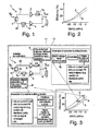
- the classical configuration of a conventional Doherty (power) amplifier arrangement 1 is shown in Fig. 1 .
- the Doherty amplifier 1 comprises a main amplification path 2a with a main amplifier 3 biased to work in class A, AB or class B mode, and an auxiliary amplification path 2b with a peak amplifier 4 biased to operate in class C mode.
- a power divider (passive splitter 5) splits an input signal S in with equal power to the main amplification path 2a and to the auxiliary amplification path 2b.
- the auxiliary amplification path 2b and the main amplification path 2a are re-combined in a power combiner (not shown) at a combining point (represented by a dot in Fig. 1 ) while guaranteeing suitable output load modulation.
- a first quarter wave section 7a is arranged in the main amplification path 2a between an output terminal of the main amplifier 3 and the combining point and a second quarter wave section 7b is arranged in the auxiliary amplification path 2b between the splitter 5 and an input terminal of the auxiliary / peak amplifier 4.
- the quarter-wave sections 7a, 7b are matched to a common center frequency of the main amplifier 3 and the peak amplifier 4 which are both adapted to operate at that center frequency by respective input and output matching networks (not shown).
- the main amplifier 3 saturates and the peak amplifier 4 takes over, thus generating an amplified output signal S out being provided to a load 6 (not being part of the arrangement).
- the Doherty amplifier arrangement 1 of Fig. 1 provides a high power-added efficiency with input signals S in that have high peak-to-average ratios.
- a measured efficiency characteristic of a Doherty amplifier arrangement mainly based on the classical concept (curve A: Drain efficiency of Doherty amplifier, and for comparison reasons curve B: balanced-mode operation (both, main and peak transistors are operated in Class-A or B mode)) in dependence of the signal power (output of a SMIQ modulator in dBm) shown in Fig. 2 differs from (i.e. is smaller than) the theoretically expected efficiency, e.g. due to the fact that the auxiliary amplifier 4 is permanently biased in Class-C mode and thus doesn't always deliver the optimum required performance for a Doherty amplifier arrangement.
- Fig. 3 shows an exemplarily embodiment of such a modified Doherty amplifier arrangement 1, additionally comprising a peak amplifier control unit 8 and a main amplifier control unit 9.
- the main amplifier control unit 9 is not restricted to controlling only the main amplifier 3, but may also be used for performing part of the control of the peak amplifier 4.
- both the main amplifier control unit 9 and the peak amplifier control unit 8 may be integrated into a single physical entity.
- the main amplifier control unit 9 is adapted for switching an (output) supply voltage V ds of the main amplifier 3 between different (discrete) voltage levels in dependence of the input signal load.
- the peak amplifier control unit 8 is provided for modulating (adaptively controlling) an input supply voltage V gs of the peak amplifier 4 in dependence of an envelope of the input signal S in and also in dependence of the (current) load.
- power transistors arranged therein may be controlled from a digital part / frontend (e.g. FPGA), which is adapted to provided the input signal S in to the Doherty amplifier arrangement 1 (after digital-to-analog conversion and possibly up-conversion) and thus has knowledge both about the load situation and about the envelope of the input signal S in .
- a digital part / frontend e.g. FPGA
- the Doherty amplifier arrangement 1 after digital-to-analog conversion and possibly up-conversion
- the control of the main amplifier 3 and of the peak amplifier 4 will be described in greater detail.
- the main amplifier 3 comprises a Field Effect Transistor, FET, and the main amplifier control unit 9 is adapted for controlling an output supply voltage V ds which represents a voltage between a drain and a source terminal of the FET.
- the main amplifier control unit 9 is also used for controlling the output supply voltage V ds of the peak amplifier 4 in a coordinated way.
- the output supply voltages V ds provided to the main amplifier 3 and the peak amplifier 4 may be chosen to be identical. It will be understood that the approach described herein is not limited to the use of FETs, and may also be applied e.g. to bipolar transistors in an analogous way.
- the load of the Doherty amplifier arrangement is defined as a difference (typically measured in dB, dBm or %) from a maximum possible power which can provided by the amplifiers 3, 4.
- Each of the different discrete levels of the output supply voltage V ds is related to a different load scenario, defined as a respective (different) range of the load of the Doherty arrangement 1.
- a different load scenario defined as a respective (different) range of the load of the Doherty arrangement 1.
- each voltage level may correspond to one of three different load conditions, e.g. low load, mid load, full load, being related to e.g. from 10 % to 40 %, from 40 % to 70 %, and from 70 % to 100 % of the full power of the Doherty arrangement 1.
- a controller may be provided for switching between the different voltage levels of the power supply 9a.
- further information e.g. about a current quality of the output signal S out of the Doherty amplifier arrangement 1, may be provided to the digital frontend and taken into account for controlling the main amplifier 3.
- the output signal may be provided to the digital frontend e.g. using a tap coupler at the output of the Doherty arrangement 1 (not shown) which may be part of a feedback-path for performing (digital) pre-distortion of the input signal S in .
- building blocks of the peak amplifier control unit 8 may e.g. comprise one or more suitable look-up tables in the digital frontend (FPGA), relating a current value of the envelope of the input signal S in to the input supply voltage V gs of the peak amplifier 4.
- a suitable interface adaptation and adaptive power supply or another suitable voltage modulator may be provided to supply the adaptive input voltage V gs to the peak amplifier 4.
- further input parameters may have an influence on the input supply voltage V gs , for example information about a current output signal quality of the Doherty amplifier arrangement 1, and, in particular, about a (current) load of the Doherty amplifier arrangement 1.
- the Doherty amplifier arrangement 1 of Fig. 3 may be used e.g. in a transmit frontend 11 of a base station 12 of a communications network (not shown), the transmit frontend 11 further comprising at least one transmit antenna for radio transmissions of the output signal S out .
- the transmit frontend 11 may in particular also comprise the digital frontend described above and further components such as digital-to-analog converters and mixers.
- the three different load scenarios (low load, mid load, high load) described above are used for the switching of the output supply voltage V ds of the main amplifier 3.
- the switching of the output supply voltage V ds in dependence of the load results in an optimized input supply voltage V gs of the main amplifier 3.
- the output supply voltage V ds of the peak amplifier 4 is also switched between (three) discrete voltage values, depending on the load condition, the switching of the output supply voltage V ds of the peak amplifier 4 may be performed either in the peak amplifier control unit 8 itself, or alternatively in the main amplifier control unit 9.
- the same multi-voltage power supply 9a may be used for providing the same switched output supply voltage V ds to both amplifiers 3, 4.
- a set of look-up tables 10a to 10c may be provided, each relating the envelope of the input signal S in to the input supply voltage V gs of the peak amplifier 4 for a different load scenario.
- a set of look-up tables 10a to 10c may be provided, each relating the envelope of the input signal S in to the input supply voltage V gs of the peak amplifier 4 for a different load scenario.
- the efficiency at back-off (supporting different load scenarios) as well as peak efficiency of the Doherty amplifier arrangement 1 may be improved by combining the two approaches in the way indicated above.
- any block diagrams herein represent conceptual views of illustrative circuitry embodying the principles of the invention.
- any flow charts, flow diagrams, state transition diagrams, pseudo code, and the like represent various processes which may be substantially represented in computer readable medium and so executed by a computer or processor, whether or not such computer or processor is explicitly shown.
Landscapes
- Engineering & Computer Science (AREA)
- Power Engineering (AREA)
- Amplifiers (AREA)
Priority Applications (1)
| Application Number | Priority Date | Filing Date | Title |
|---|---|---|---|
| EP20100290175 EP2372905B1 (de) | 2010-04-01 | 2010-04-01 | Doherty-Verstärkeranordnung mit verbessertem Wirkungsgrad |
Applications Claiming Priority (1)
| Application Number | Priority Date | Filing Date | Title |
|---|---|---|---|
| EP20100290175 EP2372905B1 (de) | 2010-04-01 | 2010-04-01 | Doherty-Verstärkeranordnung mit verbessertem Wirkungsgrad |
Publications (2)
| Publication Number | Publication Date |
|---|---|
| EP2372905A1 true EP2372905A1 (de) | 2011-10-05 |
| EP2372905B1 EP2372905B1 (de) | 2012-06-20 |
Family
ID=42779904
Family Applications (1)
| Application Number | Title | Priority Date | Filing Date |
|---|---|---|---|
| EP20100290175 Not-in-force EP2372905B1 (de) | 2010-04-01 | 2010-04-01 | Doherty-Verstärkeranordnung mit verbessertem Wirkungsgrad |
Country Status (1)
| Country | Link |
|---|---|
| EP (1) | EP2372905B1 (de) |
Cited By (7)
| Publication number | Priority date | Publication date | Assignee | Title |
|---|---|---|---|---|
| WO2015077497A1 (en) * | 2013-11-22 | 2015-05-28 | Qualcomm Incorporated | Circuits and methods for power amplification with extended high efficiency |
| WO2015157361A1 (en) * | 2014-04-09 | 2015-10-15 | Qualcomm Incorporated | Circuits and methods for biasing a power amplifier |
| WO2017212062A3 (en) * | 2016-06-10 | 2018-02-15 | Etl Systems Limited | A self-optimising rf amplifier |
| EP3993261A1 (de) * | 2020-11-02 | 2022-05-04 | Nokia Solutions and Networks Oy | Funkvorrichtung |
| WO2022197334A1 (en) * | 2021-03-19 | 2022-09-22 | Qorvo Us, Inc. | Doherty amplifier system |
| US12034470B2 (en) | 2020-11-02 | 2024-07-09 | Nokia Solutions And Networks Oy | Radio apparatus |
| US12525921B2 (en) | 2022-02-16 | 2026-01-13 | Qorvo Us, Inc. | Amplifier system |
Citations (3)
| Publication number | Priority date | Publication date | Assignee | Title |
|---|---|---|---|---|
| WO1998000912A1 (en) * | 1996-06-28 | 1998-01-08 | Motorola Inc. | Bias circuit for a power amplifier |
| EP1394932A1 (de) * | 2002-08-29 | 2004-03-03 | Postech Foundation | Doherty Verstärker |
| EP1959564A2 (de) * | 2007-02-16 | 2008-08-20 | TelASIC Communications, Inc. | System und Verfahren mit dynamischen Anpassung der Drain-Spannung zur Steuerung der Linearität- und der Ausgangsleistung- und des Wirkungsgrades in HF-Leistungsverstärkern |
-
2010
- 2010-04-01 EP EP20100290175 patent/EP2372905B1/de not_active Not-in-force
Patent Citations (3)
| Publication number | Priority date | Publication date | Assignee | Title |
|---|---|---|---|---|
| WO1998000912A1 (en) * | 1996-06-28 | 1998-01-08 | Motorola Inc. | Bias circuit for a power amplifier |
| EP1394932A1 (de) * | 2002-08-29 | 2004-03-03 | Postech Foundation | Doherty Verstärker |
| EP1959564A2 (de) * | 2007-02-16 | 2008-08-20 | TelASIC Communications, Inc. | System und Verfahren mit dynamischen Anpassung der Drain-Spannung zur Steuerung der Linearität- und der Ausgangsleistung- und des Wirkungsgrades in HF-Leistungsverstärkern |
Non-Patent Citations (2)
| Title |
|---|
| JOONGJIN NAM ET AL: "The Doherty Power Amplifier With On-Chip Dynamic Bias Control Circuit for Handset Application", IEEE TRANSACTIONS ON MICROWAVE THEORY AND TECHNIQUES, IEEE SERVICE CENTER, PISCATAWAY, NJ, US LNKD- DOI:10.1109/TMTT.2007.892800, vol. 55, no. 4, 1 April 2007 (2007-04-01), pages 633 - 642, XP011176523, ISSN: 0018-9480 * |
| JUNGHWAN MOON ET AL: "A Wideband Envelope Tracking Doherty Amplifier for WiMAX Systems", IEEE MICROWAVE AND WIRELESS COMPONENTS LETTERS, IEEE SERVICE CENTER, NEW YORK, NY, US LNKD- DOI:10.1109/LMWC.2007.912019, vol. 18, no. 1, 1 January 2008 (2008-01-01), pages 49 - 51, XP011199213, ISSN: 1531-1309 * |
Cited By (15)
| Publication number | Priority date | Publication date | Assignee | Title |
|---|---|---|---|---|
| US9231527B2 (en) | 2013-11-22 | 2016-01-05 | Qualcomm Incorporated | Circuits and methods for power amplification with extended high efficiency |
| WO2015077497A1 (en) * | 2013-11-22 | 2015-05-28 | Qualcomm Incorporated | Circuits and methods for power amplification with extended high efficiency |
| CN106134071B (zh) * | 2014-04-09 | 2019-03-19 | 高通股份有限公司 | 用于偏置功率放大器的电路和方法 |
| WO2015157361A1 (en) * | 2014-04-09 | 2015-10-15 | Qualcomm Incorporated | Circuits and methods for biasing a power amplifier |
| US9419561B2 (en) | 2014-04-09 | 2016-08-16 | Qualcomm, Incorporated | Circuits and methods for biasing a power amplifier |
| CN106134071A (zh) * | 2014-04-09 | 2016-11-16 | 高通股份有限公司 | 用于偏置功率放大器的电路和方法 |
| JP2017511079A (ja) * | 2014-04-09 | 2017-04-13 | クゥアルコム・インコーポレイテッドQualcomm Incorporated | 電力増幅器にバイアスをかけるための回路および方法 |
| WO2017212062A3 (en) * | 2016-06-10 | 2018-02-15 | Etl Systems Limited | A self-optimising rf amplifier |
| EP3993261A1 (de) * | 2020-11-02 | 2022-05-04 | Nokia Solutions and Networks Oy | Funkvorrichtung |
| CN114531168A (zh) * | 2020-11-02 | 2022-05-24 | 诺基亚通信公司 | 无线电装置 |
| US11901921B2 (en) | 2020-11-02 | 2024-02-13 | Nokia Solutions And Networks Oy | Radio apparatus |
| US12034470B2 (en) | 2020-11-02 | 2024-07-09 | Nokia Solutions And Networks Oy | Radio apparatus |
| CN114531168B (zh) * | 2020-11-02 | 2024-08-06 | 诺基亚通信公司 | 无线电装置 |
| WO2022197334A1 (en) * | 2021-03-19 | 2022-09-22 | Qorvo Us, Inc. | Doherty amplifier system |
| US12525921B2 (en) | 2022-02-16 | 2026-01-13 | Qorvo Us, Inc. | Amplifier system |
Also Published As
| Publication number | Publication date |
|---|---|
| EP2372905B1 (de) | 2012-06-20 |
Similar Documents
| Publication | Publication Date | Title |
|---|---|---|
| US8604881B2 (en) | Efficiency improvement of doherty power amplifier using supply switching and digitally controlled gate bias modulation of peaking amplifier | |
| EP2372905B1 (de) | Doherty-Verstärkeranordnung mit verbessertem Wirkungsgrad | |
| US9680434B2 (en) | Method and apparatus for calibrating an envelope tracking system | |
| US7091772B2 (en) | Power amplification by using different fixed power supply signals for the amplifier | |
| CN104170250A (zh) | 与用于包络跟踪放大器的包络路径中的成形表组合的在rf路径中的预失真 | |
| Fang et al. | Two-way Doherty power amplifier efficiency enhancement by incorporating transistors’ nonlinear phase distortion | |
| JP5217182B2 (ja) | 高周波増幅回路 | |
| Hu et al. | 2.8 A broadband CMOS digital power amplifier with hybrid class-G Doherty efficiency enhancement | |
| JP2016119664A (ja) | 動的電力供給及びデジタルプリディストーションによる効率的なマルチチャネルsatcomのためのシステム及び方法 | |
| JP2009260658A (ja) | 電力増幅器 | |
| US8054878B2 (en) | Apparatus and method for amplifying signal power in a communication system | |
| US10938358B2 (en) | Digital power amplifier | |
| US9240759B2 (en) | Amplifier assembly | |
| KR20100058189A (ko) | 무선 통신 시스템에서 신호의 송신 장치 및 방법 | |
| Banerjee et al. | High efficiency multi-mode outphasing RF power amplifier in 45nm CMOS | |
| US8145148B2 (en) | Transmitter and communication apparatus | |
| CN101167326A (zh) | 极化调制传输电路和通信设备 | |
| Komatsuzaki et al. | Advanced GaN wideband/multiband power amplifier for sub-6 GHz 5G and beyond wireless communication: Toward future flexible base station by AI-based digital assisted PA | |
| JP7281933B2 (ja) | 増幅装置 | |
| JP2012049858A (ja) | 電力増幅器 | |
| EP2475094A1 (de) | Doherty-Verstärker | |
| US20250023521A1 (en) | Doherty amplifier | |
| KR101358096B1 (ko) | 전력 증폭기 | |
| WO2021005633A1 (ja) | アウトフェージング増幅器及び通信装置 | |
| US12348190B2 (en) | Digital Doherty transmitter |
Legal Events
| Date | Code | Title | Description |
|---|---|---|---|
| PUAI | Public reference made under article 153(3) epc to a published international application that has entered the european phase |
Free format text: ORIGINAL CODE: 0009012 |
|
| AK | Designated contracting states |
Kind code of ref document: A1 Designated state(s): AT BE BG CH CY CZ DE DK EE ES FI FR GB GR HR HU IE IS IT LI LT LU LV MC MK MT NL NO PL PT RO SE SI SK SM TR |
|
| AX | Request for extension of the european patent |
Extension state: AL BA ME RS |
|
| 17P | Request for examination filed |
Effective date: 20110923 |
|
| GRAP | Despatch of communication of intention to grant a patent |
Free format text: ORIGINAL CODE: EPIDOSNIGR1 |
|
| RIC1 | Information provided on ipc code assigned before grant |
Ipc: H04W 52/18 20090101ALN20111207BHEP Ipc: H03G 3/00 20060101ALI20111207BHEP Ipc: H03F 1/02 20060101AFI20111207BHEP Ipc: H03F 3/24 20060101ALI20111207BHEP |
|
| RIC1 | Information provided on ipc code assigned before grant |
Ipc: H04W 52/18 20090101ALN20111209BHEP Ipc: H03G 3/00 20060101ALI20111209BHEP Ipc: H03F 1/02 20060101AFI20111209BHEP Ipc: H03F 3/24 20060101ALI20111209BHEP |
|
| RIC1 | Information provided on ipc code assigned before grant |
Ipc: H03F 3/24 20060101ALI20120104BHEP Ipc: H04W 52/18 20090101ALN20120104BHEP Ipc: H03F 1/02 20060101AFI20120104BHEP Ipc: H03G 3/00 20060101ALI20120104BHEP |
|
| GRAS | Grant fee paid |
Free format text: ORIGINAL CODE: EPIDOSNIGR3 |
|
| GRAA | (expected) grant |
Free format text: ORIGINAL CODE: 0009210 |
|
| RTI1 | Title (correction) |
Free format text: EFFICIENCY-IMPROVED DOHERTY AMPLIFIER ARRANGEMENT |
|
| AK | Designated contracting states |
Kind code of ref document: B1 Designated state(s): AT BE BG CH CY CZ DE DK EE ES FI FR GB GR HR HU IE IS IT LI LT LU LV MC MK MT NL NO PL PT RO SE SI SK SM TR |
|
| REG | Reference to a national code |
Ref country code: GB Ref legal event code: FG4D |
|
| REG | Reference to a national code |
Ref country code: CH Ref legal event code: EP |
|
| REG | Reference to a national code |
Ref country code: AT Ref legal event code: REF Ref document number: 563523 Country of ref document: AT Kind code of ref document: T Effective date: 20120715 |
|
| REG | Reference to a national code |
Ref country code: IE Ref legal event code: FG4D |
|
| REG | Reference to a national code |
Ref country code: DE Ref legal event code: R096 Ref document number: 602010001972 Country of ref document: DE Effective date: 20120816 |
|
| PG25 | Lapsed in a contracting state [announced via postgrant information from national office to epo] |
Ref country code: LT Free format text: LAPSE BECAUSE OF FAILURE TO SUBMIT A TRANSLATION OF THE DESCRIPTION OR TO PAY THE FEE WITHIN THE PRESCRIBED TIME-LIMIT Effective date: 20120620 Ref country code: FI Free format text: LAPSE BECAUSE OF FAILURE TO SUBMIT A TRANSLATION OF THE DESCRIPTION OR TO PAY THE FEE WITHIN THE PRESCRIBED TIME-LIMIT Effective date: 20120620 Ref country code: SE Free format text: LAPSE BECAUSE OF FAILURE TO SUBMIT A TRANSLATION OF THE DESCRIPTION OR TO PAY THE FEE WITHIN THE PRESCRIBED TIME-LIMIT Effective date: 20120620 Ref country code: NO Free format text: LAPSE BECAUSE OF FAILURE TO SUBMIT A TRANSLATION OF THE DESCRIPTION OR TO PAY THE FEE WITHIN THE PRESCRIBED TIME-LIMIT Effective date: 20120920 |
|
| REG | Reference to a national code |
Ref country code: NL Ref legal event code: VDEP Effective date: 20120620 |
|
| REG | Reference to a national code |
Ref country code: AT Ref legal event code: MK05 Ref document number: 563523 Country of ref document: AT Kind code of ref document: T Effective date: 20120620 |
|
| REG | Reference to a national code |
Ref country code: LT Ref legal event code: MG4D Effective date: 20120620 |
|
| PG25 | Lapsed in a contracting state [announced via postgrant information from national office to epo] |
Ref country code: GR Free format text: LAPSE BECAUSE OF FAILURE TO SUBMIT A TRANSLATION OF THE DESCRIPTION OR TO PAY THE FEE WITHIN THE PRESCRIBED TIME-LIMIT Effective date: 20120921 Ref country code: SI Free format text: LAPSE BECAUSE OF FAILURE TO SUBMIT A TRANSLATION OF THE DESCRIPTION OR TO PAY THE FEE WITHIN THE PRESCRIBED TIME-LIMIT Effective date: 20120620 Ref country code: HR Free format text: LAPSE BECAUSE OF FAILURE TO SUBMIT A TRANSLATION OF THE DESCRIPTION OR TO PAY THE FEE WITHIN THE PRESCRIBED TIME-LIMIT Effective date: 20120620 Ref country code: LV Free format text: LAPSE BECAUSE OF FAILURE TO SUBMIT A TRANSLATION OF THE DESCRIPTION OR TO PAY THE FEE WITHIN THE PRESCRIBED TIME-LIMIT Effective date: 20120620 |
|
| PG25 | Lapsed in a contracting state [announced via postgrant information from national office to epo] |
Ref country code: EE Free format text: LAPSE BECAUSE OF FAILURE TO SUBMIT A TRANSLATION OF THE DESCRIPTION OR TO PAY THE FEE WITHIN THE PRESCRIBED TIME-LIMIT Effective date: 20120620 Ref country code: SK Free format text: LAPSE BECAUSE OF FAILURE TO SUBMIT A TRANSLATION OF THE DESCRIPTION OR TO PAY THE FEE WITHIN THE PRESCRIBED TIME-LIMIT Effective date: 20120620 Ref country code: CZ Free format text: LAPSE BECAUSE OF FAILURE TO SUBMIT A TRANSLATION OF THE DESCRIPTION OR TO PAY THE FEE WITHIN THE PRESCRIBED TIME-LIMIT Effective date: 20120620 Ref country code: BE Free format text: LAPSE BECAUSE OF FAILURE TO SUBMIT A TRANSLATION OF THE DESCRIPTION OR TO PAY THE FEE WITHIN THE PRESCRIBED TIME-LIMIT Effective date: 20120620 Ref country code: IS Free format text: LAPSE BECAUSE OF FAILURE TO SUBMIT A TRANSLATION OF THE DESCRIPTION OR TO PAY THE FEE WITHIN THE PRESCRIBED TIME-LIMIT Effective date: 20121020 Ref country code: RO Free format text: LAPSE BECAUSE OF FAILURE TO SUBMIT A TRANSLATION OF THE DESCRIPTION OR TO PAY THE FEE WITHIN THE PRESCRIBED TIME-LIMIT Effective date: 20120620 Ref country code: CY Free format text: LAPSE BECAUSE OF FAILURE TO SUBMIT A TRANSLATION OF THE DESCRIPTION OR TO PAY THE FEE WITHIN THE PRESCRIBED TIME-LIMIT Effective date: 20120620 Ref country code: AT Free format text: LAPSE BECAUSE OF FAILURE TO SUBMIT A TRANSLATION OF THE DESCRIPTION OR TO PAY THE FEE WITHIN THE PRESCRIBED TIME-LIMIT Effective date: 20120620 |
|
| PG25 | Lapsed in a contracting state [announced via postgrant information from national office to epo] |
Ref country code: PT Free format text: LAPSE BECAUSE OF FAILURE TO SUBMIT A TRANSLATION OF THE DESCRIPTION OR TO PAY THE FEE WITHIN THE PRESCRIBED TIME-LIMIT Effective date: 20121022 Ref country code: PL Free format text: LAPSE BECAUSE OF FAILURE TO SUBMIT A TRANSLATION OF THE DESCRIPTION OR TO PAY THE FEE WITHIN THE PRESCRIBED TIME-LIMIT Effective date: 20120620 Ref country code: IT Free format text: LAPSE BECAUSE OF FAILURE TO SUBMIT A TRANSLATION OF THE DESCRIPTION OR TO PAY THE FEE WITHIN THE PRESCRIBED TIME-LIMIT Effective date: 20120620 |
|
| PG25 | Lapsed in a contracting state [announced via postgrant information from national office to epo] |
Ref country code: NL Free format text: LAPSE BECAUSE OF FAILURE TO SUBMIT A TRANSLATION OF THE DESCRIPTION OR TO PAY THE FEE WITHIN THE PRESCRIBED TIME-LIMIT Effective date: 20120620 |
|
| PLBE | No opposition filed within time limit |
Free format text: ORIGINAL CODE: 0009261 |
|
| STAA | Information on the status of an ep patent application or granted ep patent |
Free format text: STATUS: NO OPPOSITION FILED WITHIN TIME LIMIT |
|
| PG25 | Lapsed in a contracting state [announced via postgrant information from national office to epo] |
Ref country code: DK Free format text: LAPSE BECAUSE OF FAILURE TO SUBMIT A TRANSLATION OF THE DESCRIPTION OR TO PAY THE FEE WITHIN THE PRESCRIBED TIME-LIMIT Effective date: 20120620 |
|
| 26N | No opposition filed |
Effective date: 20130321 |
|
| REG | Reference to a national code |
Ref country code: DE Ref legal event code: R097 Ref document number: 602010001972 Country of ref document: DE Effective date: 20130321 |
|
| PG25 | Lapsed in a contracting state [announced via postgrant information from national office to epo] |
Ref country code: BG Free format text: LAPSE BECAUSE OF FAILURE TO SUBMIT A TRANSLATION OF THE DESCRIPTION OR TO PAY THE FEE WITHIN THE PRESCRIBED TIME-LIMIT Effective date: 20120920 |
|
| PG25 | Lapsed in a contracting state [announced via postgrant information from national office to epo] |
Ref country code: ES Free format text: LAPSE BECAUSE OF FAILURE TO SUBMIT A TRANSLATION OF THE DESCRIPTION OR TO PAY THE FEE WITHIN THE PRESCRIBED TIME-LIMIT Effective date: 20121001 |
|
| REG | Reference to a national code |
Ref country code: FR Ref legal event code: GC Effective date: 20131018 |
|
| PG25 | Lapsed in a contracting state [announced via postgrant information from national office to epo] |
Ref country code: MC Free format text: LAPSE BECAUSE OF FAILURE TO SUBMIT A TRANSLATION OF THE DESCRIPTION OR TO PAY THE FEE WITHIN THE PRESCRIBED TIME-LIMIT Effective date: 20120620 |
|
| REG | Reference to a national code |
Ref country code: IE Ref legal event code: MM4A |
|
| PG25 | Lapsed in a contracting state [announced via postgrant information from national office to epo] |
Ref country code: IE Free format text: LAPSE BECAUSE OF NON-PAYMENT OF DUE FEES Effective date: 20130401 |
|
| REG | Reference to a national code |
Ref country code: CH Ref legal event code: PCOW Free format text: NEW ADDRESS: 148/152 ROUTE DE LA REINE, 92100 BOULOGNE-BILLANCOURT (FR) |
|
| REG | Reference to a national code |
Ref country code: FR Ref legal event code: RG Effective date: 20141016 Ref country code: CH Ref legal event code: PL |
|
| PG25 | Lapsed in a contracting state [announced via postgrant information from national office to epo] |
Ref country code: CH Free format text: LAPSE BECAUSE OF NON-PAYMENT OF DUE FEES Effective date: 20140430 Ref country code: LI Free format text: LAPSE BECAUSE OF NON-PAYMENT OF DUE FEES Effective date: 20140430 |
|
| PG25 | Lapsed in a contracting state [announced via postgrant information from national office to epo] |
Ref country code: MT Free format text: LAPSE BECAUSE OF FAILURE TO SUBMIT A TRANSLATION OF THE DESCRIPTION OR TO PAY THE FEE WITHIN THE PRESCRIBED TIME-LIMIT Effective date: 20120620 |
|
| REG | Reference to a national code |
Ref country code: FR Ref legal event code: PLFP Year of fee payment: 6 |
|
| PG25 | Lapsed in a contracting state [announced via postgrant information from national office to epo] |
Ref country code: SM Free format text: LAPSE BECAUSE OF FAILURE TO SUBMIT A TRANSLATION OF THE DESCRIPTION OR TO PAY THE FEE WITHIN THE PRESCRIBED TIME-LIMIT Effective date: 20120620 |
|
| PG25 | Lapsed in a contracting state [announced via postgrant information from national office to epo] |
Ref country code: TR Free format text: LAPSE BECAUSE OF FAILURE TO SUBMIT A TRANSLATION OF THE DESCRIPTION OR TO PAY THE FEE WITHIN THE PRESCRIBED TIME-LIMIT Effective date: 20120620 |
|
| PG25 | Lapsed in a contracting state [announced via postgrant information from national office to epo] |
Ref country code: HU Free format text: LAPSE BECAUSE OF FAILURE TO SUBMIT A TRANSLATION OF THE DESCRIPTION OR TO PAY THE FEE WITHIN THE PRESCRIBED TIME-LIMIT; INVALID AB INITIO Effective date: 20100401 Ref country code: MK Free format text: LAPSE BECAUSE OF FAILURE TO SUBMIT A TRANSLATION OF THE DESCRIPTION OR TO PAY THE FEE WITHIN THE PRESCRIBED TIME-LIMIT Effective date: 20120620 Ref country code: LU Free format text: LAPSE BECAUSE OF NON-PAYMENT OF DUE FEES Effective date: 20130401 |
|
| REG | Reference to a national code |
Ref country code: FR Ref legal event code: PLFP Year of fee payment: 7 |
|
| REG | Reference to a national code |
Ref country code: FR Ref legal event code: PLFP Year of fee payment: 8 |
|
| PGFP | Annual fee paid to national office [announced via postgrant information from national office to epo] |
Ref country code: FR Payment date: 20170419 Year of fee payment: 8 Ref country code: GB Payment date: 20170419 Year of fee payment: 8 Ref country code: DE Payment date: 20170419 Year of fee payment: 8 |
|
| REG | Reference to a national code |
Ref country code: DE Ref legal event code: R119 Ref document number: 602010001972 Country of ref document: DE |
|
| GBPC | Gb: european patent ceased through non-payment of renewal fee |
Effective date: 20180401 |
|
| PG25 | Lapsed in a contracting state [announced via postgrant information from national office to epo] |
Ref country code: DE Free format text: LAPSE BECAUSE OF NON-PAYMENT OF DUE FEES Effective date: 20181101 |
|
| PG25 | Lapsed in a contracting state [announced via postgrant information from national office to epo] |
Ref country code: GB Free format text: LAPSE BECAUSE OF NON-PAYMENT OF DUE FEES Effective date: 20180401 |
|
| PG25 | Lapsed in a contracting state [announced via postgrant information from national office to epo] |
Ref country code: FR Free format text: LAPSE BECAUSE OF NON-PAYMENT OF DUE FEES Effective date: 20180430 |